
Related Manuals for LG LAC2900N


Summary of Contents for LG LAC2900N
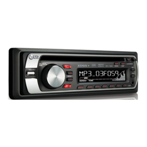
- Page 1 Internal Use Only Website http://biz.lgservice.com CAR CD/MP3/WMA RECEIVER SERVICE MANUAL MODEL : LAC2900N CAUTION BEFORE SERVICING THE UNIT, READ THE “SAFETY PRECAUTIONS” IN THIS MANUAL. P/NO : AFN73228921 JUNE, 2009...
-
Page 2: Table Of Contents
CONTENTS SECTION 1 SUMMARY SERVICING PRECAUTIONS ..........................1-2 ESD PRECAUTIONS ............................1-3 SPECIFICATIONS ..............................1-4 FIRMWARE UPGRADE METHOD ........................1-5 HOW TO CONNECT AUDIO SET TO POWER SUPPLY ..................1-6 SECTION 2 ELECTRICAL ELECTRICAL TROUBLESHOOTING GUIDE & WAVEFORMS ...............2-1 1. SYSTEM CONTROL ERROR CORRECTION FLOW CHART ..............2-1 2. -
Page 3: Servicing Precautions
SECTION 1 SUMMARY SERVICING PRECAUTIONS 1. Always disconnect the power source before: 1) Removing or reinstalling any component, circuit board, module or any other instrument assembly. 2) Disconnecting or reconnecting any instrument electrical plug or other electrical connection. 3) Connecting a test substitute in parallel with an electrolytic capacitor in the instrument. CAUTION: A wrong part substitution or incorrect polarity installation of electrolytic capacitors may result in an explosion hazard. -
Page 4: Esd Precautions
ESD PRECAUTIONS Electrostatically Sensitive Devices (ESD) Some semiconductor (solid state) devices can be damaged easily by static electricity. Such components com- monly are called electrostatically sensitive devices (ESD). Examples of typical ESD devices are integrated circuits and some fi eld-effect transistors and semiconductor chip components. The following techniques should be used to help reduce the incidence of component damage caused by static electricity. -
Page 5: Specifications
SPECIFICATIONS • GENERAL Output Power 53 W x 4 CH (Max.) Power Source DC 12V Speaker impedance 4Ω Ground System Negative Dimensions (W x H x D) 180 x 50 x 176 mm (Without Control Panel) Net Weight 1.3kg • TUNER Frequency Range 87.5 ~ 107.9, 87.5 ~ 108MHz S/N Ratio... -
Page 6: Firmware Upgrade Method
FIRMWARE UPGRADE METHOD [ MAIN/CD FIRMWARE UPGRADE ] 1. Confi rmation of version information • Change the Source of audio set to tuner. (Default: tuner) • Turn power off using power key. • Press power key for 5 sec. (After power on, continue pressing) •... -
Page 7: How To Connect Audio Set To Power Supply
HOW TO CONNECT AUDIO SET TO POWER SUPPLY • It is suffi cient only to supply power for upgrade. • Shown from the right fi gure, connect yellow line (Battery) and red line (Ignition) to plus and minus terminal respectively. •... -
Page 8: Electrical Troubleshooting Guide & Waveforms
SECTION 2 ELECTRICAL ELECTRICAL TROUBLESHOOTING GUIDE & WAVEFORMS 1. SYSTEM CONTROL ERROR CORRECTION FLOW CHART Something wrong with the system control? No power? F301 Inside of CN302 Checked the Fuse? Checked the Back up CN301(16,15) Vdd and Gnd? Checked the Regulator IC301(15,14) Back up Vdd ? Checked the Main Micom... - Page 9 Not available to Volume control? Checked the RV901, CN901(2,4), IC402(82,83) Encoder Volume? Checked the IC402(9,10), IC802(25,26) Volume IC control? Not available to Key Control? Checked the SW902~SW918 Tact switch? Checked the CN901(11,13), IC402(53,54) Key line? Not available to ANT(Motor Type) Control? Checked the D430, IC301(12,13), IC402(33) ANT control?
-
Page 10: Sound Error Correction Flow Chart
2. SOUND ERROR CORRECTION FLOW CHART Something wrong with the Sound? No sounds of All Functions? Checked the IC802(24) E-VR Vdd? Checked the IC802(27) E-VR Ground? Checked the IC802(25,26), IC402(9,10) E-VR Control? Checked the E-VR IC802(15), IC402(15) Mute Control? Checked the E-VR IC802(1,2,3,4,5,6,7,9,18,19,20,21,22,23) Signal in/out? Checked the... - Page 11 Hearing the Pop Noise? IC402(14,15,23,32), IC802(15) Checked the IC801(22), Q601, Q602, Q603, Q604,Q605, Mute Contorl? Q606, Q607, Q608, Q609, Q610 Checked the TU201(8), IC402(7) AF mute? No output Beep sound? Checked the IC402(80), IC802(14) Beep Control?
- Page 12 ■ CAUTION - Tip for repair Before exchange power amp IC(TB2946) for no audio problem, you have to check below list. 1. Check VCC (pin 20,6) & GND 2. Check input pin 11,12,14,15 OUT1 + 3. Check Standby, pin 4 PW-GND1 : Follow the below list.
-
Page 13: Display Error Correction Flow Chart
3. DISPLAY ERROR CORRECTION FLOW CHART Something wrong with the Display? No Display or Some Display is broken? Checked the LCD IC901(56) Driver Vdd? Checked the LCD IC901(60) Driver Ground? Checked the LCD IC901(57), IC402(79) Driver RESET? Checked the LCD IC901(61) Driver OSC? Checked the LCD... - Page 14 Not available to illumination with button? Checked the Dimmer CN302(7), IC301(9) control input? Checked the IC301(4) LED Vdd? Checked the LD901, LD904~LD919 RED LED?
- Page 15 Don't moved Level dancing bar? Checked the Level IC802(17), IC402(57) Meter Signal Input? Not avaliable to LCD Lighting control Checked the Dimmer CN302(7), IC301(9), D423, IC402(43,49) control input? Checked the IC301(4), Q305, CN901(16) LCD Vdd? Checked the LCD Q317, IC402(41) Vdd control? LD902, LD903 Checked the LED?
-
Page 16: Tuner Error Correction Flow Chart
4. TUNER ERROR CORRECTION FLOW CHART Something wrong with the Tuner system? Not available to Tuner? Checked the TU201(6,17), Q302, IC301(10,14) Tuner Vdd? Checked the Tuner IC402(40), Q307, IC301(11) Vdd control? Checked the TU201(3,7,12,16) Tuner Ground? Checked the TU201(14,15), IC402(34,36) I2C data? Checked the TU201(1,2) - Page 17 Tuner no sound? Checked the TU201(10,11), IC802(5,6) Tuner Signal out? Checked TU201(8), IC402(7) the AF mute? Checked the See the Sound Error correction Process. E-VR & Power AMP? Not available to AF? Checked the TU201(4), IC402(56) S-METER level? Checked TU201(19,20), IC402(5,6) the RDS data? Not available to RDS function? Checked...
-
Page 18: Cdp Error Correction Flow Chart
5. CDP ERROR CORRECTION FLOW CHART Something wrong With the CD Player? No Loading? CN520(12,16) Checked the CD Vdd? Checked the CD IC503(28,42,60,72,81,123,143) DSP Ground? Checked the Motor IC504(7,8,20) DRV VDD? Checked the CD IC504(88) DSP Reset? Checked the CD X501 DSP X-tal? Checked the Disc in... - Page 19 No Reading & "FILE CHECK" DISPLAY? Checked the CN506(8) Limit switch? Fig 1, 2 Checked the Motor IC504(21) DRV mute control? Checked the Motor CN520(19,21) LODING Control? Fig 3, 4 Checked the CD IC503(84,85,86,87) DSP Control? Fig 10~ 11 Checked the IC503(38), IC504(15,16) focus Control? Fig 5...
- Page 20 CD no sound? Checked the IC503(140,141) DSP signal out? No ejected the CD? Checked the IC402(54) Eject key? Checked the Loading CN520(19,21) Motor Control? Fig 3,4 2-13...
-
Page 21: Aux Error Correction Flow Chart
6. AUX ERROR CORRECTION FLOW CHART Something wrong With the AUX? AUX no sound? Checked the AUX JK901, CN901(6,10), L901, L902, R603, R604 Signal input? Checked the See the Sound Error correction Process. E-VR & Power AMP? 2-14... -
Page 22: Waveforms
• WAVEFORMS Fig.1) SWITCHING CONDITION FOR LOADING Fig.2) SWITCHING CONDITION FOR UNLOADING CN520:[PIN7] CN520:[PIN7] CN520:[PIN30] CN520:[PIN30] CN520:[PIN29] CN520:[PIN29] LOADING S/W LOADING S/W CN520:[PIN27] CN520:[PIN27] 12/8 S/W 12/8 S/W LIMIT S/W LIMIT S/W CHUCKING S/W CHUCKING S/W Fig.3) MOTOR CONTROL SIGNAL FOR LOADING Fig.4) MOTOR CONTROL SIGNAL FOR UNLOADING CN520:[PIN19] CN520:[PIN19]... - Page 23 Fig.7) SPINDLE CONTROL SIGNAL Fig.8) SLED CONTROL SIGNAL IC503:[PIN41] IC503:[PIN40] IC503:[PIN25] IC504:[PIN13] IC504:[PIN11] IC504:[PIN14] IC504:[PIN12] SPOUT SLOUT Fig.9) MD, RFOUT, LD Fig.10) DI, DO, CL, CE CN519:PIN[15] IC503:DO(PIN87) IC503:PIN[8] IC503:DI(PIN86) CN519:PIN[16] IC503:CL(PIN85) IC503:CE(PIN84) RFOUT Fig.11) DI, DO, CL, CE [Detail] Fig.12) FSEQ, WRQ IC503:DO(PIN87) CN520:(PIN24)
-
Page 24: Circuit Voltage Chart
• CIRCUIT VOLTAGE CHART Operating Operating Operating Pin No. Pin No. Pin No. Voltage (V) Voltage (V) Voltage (V) IC301_HA13173 4.96 1.54 2.52 13.92 2.52 5.06 8.46 0.02 5.05 8.05 5.01 3.284 13.99 5.06 0.063 4.31 CN302_ISO 16Pin 13.98 4.94 6.56 5.76 6.57... -
Page 25: Internal Block Diagram Of Ics
INTERNAL BLOCK DIAGRAM OF ICs 1. IC301 (HA13173AH) 1-1. BLOCK DIAGRAM DBUP 100uF 0.1uF Over voltage detect VBUP 3.5V CTL 1 CBUP 100uF BIAS 1.5V CTL 2 2.5V CTL 3 VDDOUT CVDD 2.5V 10uF CTL 4 2.5V DSPOUT CDSP EXTOUT DEXT1 10uF DEXT2... - Page 26 1-2. PIN FUNCTION (Note1) Protection function Pin No. Pin name Function Normal (Note2) (Note3) (Note3) TSD On VB=24V VB=50V operation Ground FREG_B External Trs bass drive (Note4) On/Off On/Off FREG_F FREG feedback terminal On/Off On/Off ILMOUT 8.4V output for JLM/500mAmax On/Off CTL4 FREG control terminal...
- Page 27 2. IC402 (μPD78F1164) 2-1. PIN CONFIGURATION 100 99 98 97 96 95 94 93 92 91 90 89 88 87 86 85 84 83 82 81 P60/SCL0 P140/PCLBUZ0/INTP6 P61/SDA0 P141/PCLBUZ1/INTP7 P142/SCK20/SCL2 P143/SI20/RxD2/SDA2 P31/TI03/TO03/INTP4 P144/SO20/TxD2 P64/RD P145/TI07/TO07 P65/WR0 P00/TI00 P66/WR1 P01/TO00 P67/ASTB P02/SO10/TxD1 P77/EX23/KR7/INTP11...
- Page 28 2-2. PIN DESCRIPTION Enable Output Name in Micom Name in Model Description setted Format P60/SCL0 EEPROM_CLK(O) N-CH B/T EEPROM CLOCK OUT P61/SDA0 EEPROM_DATA(O) N-CH B/T EEPROM DATA OUT PLL_CLK(O) N-CH CLK output for PLL IC PLL_DATA(O) N-CH Data input for PLL IC P31/TI03/TO03/INTP4 RDS_CLK(I) From tuner pack, RDS CLK input...
- Page 29 Enable Output Name in Micom Name in Model Description setted Format P111/VNO1 LCD_LIGHT(O) CMOS LCD Light control AVREF0 AVREF0 • D/A converter reference voltage input • Positive power supply for P110, P111, and D/A converter AVSS AVSS Ground Potential for Ports P157/ANI15 WIREDREMOCON_ADIN(I) Wired RMC line input...
-
Page 30: Ic503 (Lc786923W)
3. IC503 (LC786923W) 3-1. PIN CONFIGURATION 2-23... - Page 31 3-2. BLOCK DIAGRAM 2-24...
- Page 32 3-3. PIN DESCRIPTION 2-25...
- Page 33 2-26...
- Page 34 2-27...
-
Page 35: Ic504 (Am5810)
4. IC504 (AM5810) 4-1. PIN CONFIGURATION AM5810 4-2. BLOCK DIAGRAM CH1~CH4 MUTE POWVCC34 (CH3, CH4) 7.5K LEVEL 7.5K SHIFT LEVEL SHIFT 7.5K LEVEL LOADING PRE SHIFT FWD REV LEVEL 7.5K SHIFT PREVCC POWVCC12 POWER (PRE, LOADING) (CH1, CH2) SAVE 2-28... - Page 36 4-3. PIN DESCRIPTION Pin No. Pin Name Pin Description Input for loading forward Input for loading reverse LDCONT Output control terminal for loading Control terminal for power saving mode Input 1 of CH1 Input 2 of CH2 PREVCC Pre and loading unit power supply input terminal POWVCC12 Power unit power supply input terminal (CH1, CH2) VOL ( - )
-
Page 37: Ic801 (Tb2946Hq)
5. IC801 (TB2946HQ) 5-1. BLOCK DIAGRAM Ripple Out1 (+) PW-GND1 Out1 (-) Out2 (+) PW-GND2 Pre-GND Out2 (-) Out3 (+) PW-GND3 Out3 (-) AC-GND Out4 (+) PW-GND4 4 Stby Out4 (-) Play Mute 22 Mute Offset/short 2-30... -
Page 38: Ic802 (Bd3702Fv)
6. IC802 (BD3702FV) 6-1. BLOCK DIAGRAM 6-2. PIN DESCRIPTION Terminal Terminal Terminal Terminal Description Description Name Name A input terminal of 1ch MUTE External compulsory mute terminal A input terminal of 2ch LRST Level meter reset terminal B input terminal of 1ch LOUT Output terminal for Level meter B input terminal of 2ch... -
Page 39: Ic901 (Mc5502)
7. IC901 (MC5502) 7-1. PIN CONFIGURATION 7-2. BLOCK DIAGRAM 2-32... - Page 40 7-3. PIN DESCRIPTION Pin No. Pin Name Pin Description 1 ~ 12 SEG1/ P1 ~ LCD Segment output pins / General-purpose output pins(Only 1/4Duty Mode) SEG12/ P12 Select Segment output pins or General-purpose output pins by the instruction. 13 ~ 51 SEG13~SEG51 LCD Segment output pins.
- Page 41 MEMO 2-34...
-
Page 42: Wiring Diagram
WIRING DIAGRAM 2-35 2-36... -
Page 43: Block Diagram
BLOCK DIAGRAM 2-37 2-38... -
Page 44: Circuit Diagrams
CIRCUIT DIAGRAMS 1. MAIN CIRCUIT DIAGRAM 2-39 2-40... -
Page 45: Front Circuit Diagram
2. FRONT CIRCUIT DIAGRAM 2-41 2-42... -
Page 46: Cdp Circuit Diagram
3. CDP CIRCUIT DIAGRAM 2-43 2-44... -
Page 47: Printed Circuit Board Diagrams
PRINTED CIRCUIT BOARD DIAGRAMS 1. MAIN P.C.BOARD (TOP VIEW) (BOTTOM VIEW) 2-45 2-46... -
Page 48: Front P.c.board
2. FRONT P.C.BOARD (TOP VIEW) (BOTTOM VIEW) 2-47 2-48... -
Page 49: Cdp P.c.board
3. CDP P.C.BOARD ( TOP VIEW ) ( BOTTOM VIEW ) 2-49 2-50... -
Page 50: Cabinet And Main Frame Section
SECTION 3 EXPLODED VIEWS 1. CABINET AND MAIN FRAME SECTION Accessory Loc.No. Loc.No. Loc.No. Loc.No. FRONT LCD901 MAIN... -
Page 51: Mechanism(Pick-Up) Section
2. MECHANISM(PICK-UP) SECTION...
Need help?
Do you have a question about the LAC2900N and is the answer not in the manual?
Questions and answers