
Related Manuals for LG GWA-4161B


Summary of Contents for LG GWA-4161B
- Page 1 DVD/CD Rewritable Drive S E RVICE MANUAL MODEL: GWA - 4 1 6 1 B P/NO : 3828HS1049B N o v e m b e r, 2004 Printed in Korea MODEL : GWA-4161B...
-
Page 2: Table Of Contents
TABLE OF CONTENTS INTRODUCTION ..................................3 FEATURES....................................3~4 SPECIFICATIONS.................................5~8 LOCATION OF CUSTOMER CONTROLS .........................9~10 DISASSEMBLY .................................11~12 1. CABINET and CIRCUIT BOARD DISASSEMBLY ......................11 1-1. Bottom Chassis ................................11 1-2. Front Bezel Assy ................................11 1-3. Cabinet and Main Circuit Board ..........................11 2. MECHANISM ASSY DISASSEMBLY..........................11 2-1. -
Page 3: Introduction
INTRODUCTION read as much as 700 Mbytes of digital data stored This service manual provides a variety of service in a CD-ROM, CD-R and CD-RW disc. information. It can write as much as 4.7Gbytes of digital data It contains the mechanical structure of the DVD/CD into DVD+R/RW disc, and can read as much as Rewritable Drive and the electronic circuits in 4.7Gbytes of digital data stored in a DVD-ROM,... - Page 4 4. Performance 1) Average access time : CD-ROM 120ms (Random) DVD-ROM 140ms(SL) 2) Write speed : CD-R 10x, 16x CLV, 24x ZCLV, 40x CAV CD-RW 4x, 10x, 16x CLV, 24x ZCLV (High Speed CD-RW supported: 8x, 10x, Ultra Speed CD-RW supported: >16x) DVD-R 2x, 4x CLV, 8x ZCLV DVD-RW 1x, 2x, 4x CLV DVD+R 2.4x, 4x CLV, 8x ZCLV, 12x, 16x CAV...
-
Page 5: Specifications
SPECIFICATIONS 1. SYSTEM REQUIREMENTS -CPU: IBM Compatible Pentium4 1.6GHz (or faster) (For High speed, 2GHz or faster recommended.) -128MB Memory or greater 2. SUPPORTING OPERATING SYSTEM * Operating System * Recording tool Window 98 Second Edition (1) RecordNow (Sonic) Windows Millennium Edition (Me) (2) DLA (sonic) Window 2000 Professional (3) Nero(Ahead) - Page 6 2.3 Disc diameter ..........120mm 80mm (Horizontal only) 2.4 Data capacity • User Data/Block DVD-ROM/R/RW/+R/+RW ....2,048 bytes/block CD (Yellow Book) ..........2,048 bytes/block(Mode 1 & Mode 2 Form 1) 2,336 bytes/block (Mode 2) 2,328 bytes/block (Mode 2 Form 2) 2,352 bytes/block (CD-DA) 2.5 RPC (Regional Playback Control) Phase2, No Region 3.
- Page 7 3.3 Data transfer rate 3.3.1 Sustained transfer rate <Read> CD-ROM/R.............2,550 ~ 6,000 kbytes/s (40x) Max. CD-RW............2,250 ~ 4,800 kbytes/s (32x) Max. CD-DA(DAE) ..........2,250 ~ 4,800 kbytes/s (32x) Max. DVD-ROM ....Single layer......9.28 ~ 22.16 Mbytes/s (16x) Max. Dual layer ......4.58 ~ 11.08 Mbytes/s (8x) Max. DVD-R............5.73 ~ 13.85 Mbytes/s (10x) Max.
-
Page 8: Quality And Reliability
3. Ambient temperature : Normal temperature 4. Except loading, unloading and seek 8. Dimensions External dimensions (W x H xD) 146x41.3x184.7mm Front bezel (WxHxD) 148x42x5 mm 9. Mass ..........880g+/-10g(net) * Please Contact the friendly staff of LG Service Care at: Website http: //www.LGEservice.com... -
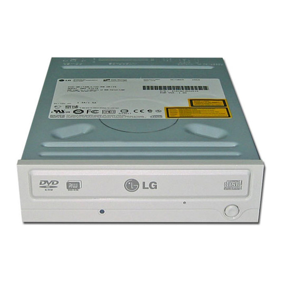
Page 9: Location Of Customer Controls
LOCATION OF CUSTOMER CONTROLS Front Panel Emergency Eject Hole Disc Tray Stop/Eject Button Drive Activity Indicators 1. Disc tray 3. Emergency Eject Hole This is the tray for the disc. Place the disc on the Insert a paper clip here to eject the Disc tray ejected disc tray, then lightly push the tray (or manually or when there is no power. -
Page 10: Rear Panel
Rear Panel IDE Interface Connector Analog Audio Output Connector Jumper Connector Power Connector Digital Audio Output Connector 1. Power Connector 3. Jumper Connector Connects to the power supply (5-and 12-V DC) of This jumper determines whether the drive is the host computer. configured as a master or slave. -
Page 11: Disassembly
DISASSEMBLY 1. CABINET and CIRCUIT BOARD 1-3. Cabinet and Main Circuit Board A. Remove the Cabinet in the direction of arrow (4). DISASSEMBLY (See Fig. 1-3) 1-1. Bottom Chassis B. Release 2 hooks (a) and remove the CD Tray A. Release 4 screws (A) and remove the Bottom Chassis drawing forward. -
Page 12: Pick-Up
2-2. Pick-up A. Release 1 screw (C) and remove the Pick-up. Pick-up Unit Pick-up Fig. 2-2... -
Page 13: Exploded View
EXPLODED VIEW PBM00 (MAIN C.B.A) PBF00 (FRONT C.B.A) -
Page 14: Glossary
GLOSSARY ATIP Absolute Time in Pre-groove. With an additional modulation of the “Wobble”, the “Groove” contains a time code information. Wobble The pre-groove in the Disc is not a perfect spiral but is wobbled. With : – A typical amplitude of 30 nm –... -
Page 15: The Differences Of Cd-R/Cd-Rw Discs And General Cd-Rom
The differences of CD-R/CD-RW discs and General CD-ROM 1. Recording Layer Recordable CD has a wobbled pre-groove on the surface of disc for laser beam to follow track. Track pitch(p) a=30nm Read-only Disc CD-ROM (READ-ONLY DISC) Radial Direction Radial Error Signal 0.4~0.5 um Groove Land... -
Page 16: Disc Materials
3. Disc Materials 1) CD-ROM disc • It is composed of Silver _ colored aluminum plate and Reflective layer. • Groove (Pit) of aluminum plate make a track. • Laser wavelength : 780 nm, Laser Power (Read): 0.5mW • Signal is detected by the difference of reflective beam intensity between “pit”... -
Page 17: Reading Process Of Optical Disc
3) CD-RW Disc Label Printing Protective Layer Dielectric Layer(TL) Recording Layer Dielectric Layer(UL) Substrate (Polycarbonate) Groove Laser Beam • It is composed of polycarbonate layer, alloy(silver, arsenic) layer, aluminum reflectivity layer, protective layer. • An crystalized alloy layer is transformed into noncrystalized by the laser heat. Therefore, writing and reading is enabled by the difference of reflectivity. -
Page 18: Writing Process Of Cd-R Disc
5. Writing Process of CD-R Disc Incident (Write) Laser Power (Read) (Read) Laser Spot a b c d e f Position (Time) Laser Below "ORP"– Mark Too Short Spot Reflected At Optimum Record Power ("ORP") Light Signal Above "ORP" – Mark Too Long Recorded Mark Time... -
Page 19: Organization Of The Pca, Pma And Lead-In Area
7. Organization of the PCA, PMA and Lead-in Area 1) Layout of CD-ROM disc Disc Center Diameter 120 mm Diameter 46 mm Diameter 15 mm Center hole Clamping and Label Area Information Area Read Only Disc Lead-in Area Program Area Lead-out Area 2) Layout of CD-R/RW disc Disc Center... -
Page 20: Function Of Pca And Pma Area
8. Function of PCA and PMA area 1) PCA (Power Calibration Area) • PCA area is used to determine the correct Laser Power for a disc. – Method 1 : PCA area is divided by a track. – Method 2 : The previous Calibration value is referred. –... -
Page 21: Writing Process Of Disc
2) ROPC (Running Optimum Power Control) • Variable primary factor of Optimum Power – Change of Power sensitivity on the Disc. (limited to 0.05 *Po) – Wavelength shift of the laser diode due to the operating temperature change. – Change of the Spot aberration due to the Disc skew, Substrate thickness, Defocus. -
Page 22: The Differences Of Dvd-R/Rw, Dvd+R/Rw Discs And Dvdd-Rom
The differences of DVD-R/RW, DVD+R/RW discs and DVD-ROM 1. Recording Layer DVD-ROM (Read Only Disc) 0.4 um DVD-R/RW Disc (Land Pre-Pit) DVD+R/RW Disc... -
Page 23: Disc Specification
2. Disc Specification DVD-ROM DVD-R DVD-RW DVD+R DVD+RW Single-Layer Dual-Layer Media Type Read Only Read Only Phase change Phase change User data capacity 4.7GB 8.54GB 4.7GB 4.7GB 4.7GB 4.7GB Wavelength 650nm 650nm 650nm 650nm 650nm 650nm Reflectivity 45~85% 18~30nm 45~85% 18~30% 45~85% 18~30nm... - Page 24 2) Recording format using organic dye material (DVD-R/DVD+R) * The format that records data through the creation of recorded marks by changing the organic dye material with a laser beam. > Disc structure DVD-R DVD+R Adhesive layer Adhesive layer Protective layer Protective layer Reflective layer Reflective layer...
- Page 25 3) Recording format using phase-change recording material (DVD-RW/DVD+RW) * Data is recorded by changing the recording layer from the amorphous status to the crystalline status, and played back by reading the difference of the reflection coefficient. [ Amorphous : Non-crystalline ] >...
-
Page 26: Writing Pulse Waveform Of Dvd+R
4. Writing Pulse Wave Form of DVD+R For different speed ranges, different write strategies can be used. This document specifies 2 options: - a pulsed write strategy, where each single mark is created by a number of subsequent separated short pulses. - Page 27 2) 2 Method : Using Blocked Write Strategy NRZI Channel bits 1.25T top,3 1.25T 3T mark top,3 top,4 1.25T 4T mark top,4 1.25T 5T mark top,4 1.25T Etc. top,4 N = 3 : T (cm = 3) can be optimized individually. N >...
-
Page 28: Writing Pulse Waveform Dvd+Rw
5. Writing Pulse Wave Form of DVD+RW NRZI Channel bits Ttop dTera dTtop Pp : Actual write power Pe : Erase Power Pb : Bias Power... -
Page 29: Organization Of Inner Drive Area, Outer Drive Area, Lead-In Zone And Lead-Out Zone
6. Organization of the Inner Drive Area, Outer Drive Area, Lead-in Zone and Lead-out Zone 1) Layout of DVD-ROM disc Disc Center Diameter 120 mm Diameter 44 mm Diameter 33 mm Diameter 22 mm Diameter 16 mm Diameter 15 mm Clamping Center 3rd transtion... - Page 30 3) Layout of DVD+RW disc Disc Center Diameter 120 mm Diameter 44 mm Diameter 33 mm Diameter 22 mm Diameter 16 mm Diameter 15 mm Clamping Center 3rd transtion Information Zone Zone hole area 1st transition area Rim area 2nd transition area Unrecorded Disc Lead -out Zone Lead-in Zone...
-
Page 31: Dvd & Cd Data Processing
DVD & CD DATA PROCESSING 1. Data Processing Flow... -
Page 32: Copy Protection And Regional Code Management Block
2. Copy Protection and Regional Code Management Block Block Diagram Change the "KEY" HOST DVD MN103S86G PLAYER (EMPEG2 B/D) Scrambled MPEG Data KEY Management Control Brief Process 1. Regional Code for DVD Disc – DVD-ROM drive transfers the regional code of the control data to host by the command of host, the DVD player of host reads the regional code, and plays title in the case of allowed regional code only. -
Page 33: About Prevention The Dvd-Rom From To Be Copy
3. About Prevention the DVD-ROM from to be copy A data is able to encode and record in the disc, if a copyright holder wants to prevent the disc from copying. In case of a disc enhanced movie of 3 titles..DISC KEY (2048 Bytes) is used to encode the whole contents in the disc and TITLE KEY (5 Bytes) is used to encode the title respectively. -
Page 34: About The Dvd-Rom Regional Code
4. About the DVD-ROM Regional Code Regional code U.S.A PRI. VIR DISC ROM - DRIVE MPEG-2 BOARD VGA CARD MONITOR Transfer to Receiving If the board is setting to the regional The disc has MPEG-2 board data from the code 1 for the U.S.A..the regional reading the MPEG-2... -
Page 35: Internal Structure Of The Pick-Up
INTERNAL STRUCTURE OF THE PICK-UP 1. Block Diagram of the PICK-UP(HOP-7531TS) Tilt- 44 Tilt+ 43 TR- 42 TR+ 41 AF- 4700p 4.7k 40 AF+ R2 2.7k 39 GND(LDD) R4 360k IC1 EL6938CL 16 15 14 13 12 11 10 38 ENA 37 SLG CD LD 36 IAPC... -
Page 36: Pick Up Pin Assignment
2. Pick up Pin Assignment Signal Name Signal Description GND(OEIC) Ground for OEIC Vcc(OEIC) Power supply for OEIC(+5V) Vc(OEIC) Reference voltage input for OEIC(+2.3V) GAINSW OEIC output gain control (High:Low gain, Middle:Middle gain, low:High gain) E3+F3 Single OEIC output ED3 Single OEIC output B Single OEIC output D E4+F4... -
Page 37: Signal Detection Of The P/U
3. Signal detection of the P/U Infrared Iaser Pick-Up module Focusing Tracking Photo Diode 1) Focus Error Signal ==> (A+C)-(B+D) This signal is generated in RF IC (IC121 : AN22112A) and controls the pick-up’s up and down to focus on Disc. -
Page 38: Description Of Circuit
DESCRIPTION OF CIRCUIT 1. ALPC (Automatic Laser Power Control) Circuit 1-1. Block Diagram IC 121 CN 101 AN22112A IC 201 VREFPD Optical MN103S86G Pick-up S/H2 HOP-7531TS 127 FPDM Erase S/H3 Space S/H1 Write Strategy Signal Serial ADSC 1-2. ALPC (Automatic Laser Power Control) Circuit Operation The ALPC block detects the laser output power of the front monitor. -
Page 39: Focus/Tracking/Sled Servo Circuit
2. Focus/Tracking/Sled Servo Circuit 2-1. Focus, Tracking & Sled Servo Process Focus, Tracking, Sled Servo Pick-up Focus Error Detector A,B,C,D A,B,C,D E,F,G,H Focus Error Detector A,B,C,D E,F,G,H IC121 A N22112A IC201 Tracking Focusing Servo Control Actuator MN103S86G LEVEL SHIFT FDRV PARALLEL LEVEL SHIFT DIGITAL... -
Page 40: Spindle Servo Circuit
3. Spindle Servo Circuit 3-1. Spindle Servo Process IC121 AN22112A Pick-up Wobble Signal WBLIN Generator IC201 MN103S86G Spindle Motor SERVO DSP Frequency Controller SPDRV Phase Controller IC301 BD7954FS 3-2. Spindle Servo Spindle servo is as following ; Wobble CLV 4x, 10x, 16x, 24x, 32x, 40x : Blank area in CD-R, CD-RW Wobble CLV 1x, 2x, 2.4x, 4x, 8x : Blank area in DVD+/-R/RW CD 15x CAV : Video CD, CD-DA(Audio out) CD 32x CAV : CD-RW, CD-DA(DAE) -
Page 41: Major Ic Internal Block Diagram And Pin Description
MAJOR IC INTERNAL BLOCK DIAGRAM AND PIN DESCRIPTION IC121 (AN22112A) : FEP(RF) Analog Signal Processor • Pin Assignment CLUMPGT CDRFP CDRFN LPPS CDHPF ASENV/LPPM DLY1 GND4 DLY2 VCC52 GND2 RSDAT RSEN SDAT AN22112A VCC4 (Top View) 128Pin TQFP VCC1 WIDGT/SH4 VREF SVREF TQFP-128-P-1414A... - Page 42 Block Diagram Operation Circuit...
- Page 43 • Pin Assignment Pin no. Pin Name Type Function Ground pin for APC/OPC & ASENV ROPCIN Input pin after OPC addition APCAAF1 Capacitor connection pin for APC mark system AAF APCAAF2 Capacitor connection pin for APC average DC detection system AAF APCAAF3 Capacitor connection pin for APC bottom detection system AAF.
- Page 44 Pin no. Pin Name Type Function OFTR Off-track signal output BDO output VCC51 Power supply pin for CMOS I/F 1(3.3V) GND5 Ground pin for CMOS I/F WTGT Write gate signal input (pull-down) FEPIDGT/SH6 CAPA through signal input pin for DVD-RAM/Main beam sample-and-hold timing signal input pin(pull-dowm) POLGT/SH7 CAPA polarity selection input pin for DVD-RAM/Sub beam sample-and hold...
- Page 45 Pin no. Pin Name Type Function RFIN2 RFAGC signal input pin 2 RFIN1 RFAGC signal input pin 1 HDVREF 2.2V reference voltage output pin CWBLBUF Capacitor connection pin for WBLDIF VCC2 Power supply pin for RFGene/RFEQ/WBL/LPP (5.0V) RFOUT RFGene signal output pin CLPPPH Capacitor connection pin for LPP peak hold CLPPHPF...
- Page 46 Pin no. Pin Name Type Function CD main signal input pin 1 CD main signla input pin 2 CD main signal input pin 3 CD main signla input pin 4 CD sub signal input pin 1 CD sub signll input pin 2 CD sub signla input pin 3 CD sub signla input pin 4 DACOUT...
- Page 47 IC201 (MN103S86G) : Encoder, Decoder & DSP Singal Processor • Pin Assigment BSMD FADR3 NBSMD FADR2 PKMD FADR1 NPKMD PK2MD MPK2MD PK3MD NPK3MD AVDD33D2 LOUT ROUT AVSSD2 VDD3 VREFH MN103S86G AVDD33D1 MA10 CPOP5 CPOP4 P15/TRCDATA3/EXTR1G2/MBA1 CPOP3 P14/TRCDATA2/EXTR1G1/MA11 CPOP2 MBA0 (MN103SEM0T86) CPOP1 MCKB AVSSD1...
- Page 48 • Block Diagram (SODC:MN103S86G) HOST HOST SDRAM SERVO 16 Mbit ADSC ANALOG 64 Mbit 16.9MHz PERIPHERAL Falsh 32 bit CPU 2 Mbyte...
- Page 49 • Pin Table Pin Name Connection Description Number Target BSMD BIAS modulation signal differential current output NBSMD NBIAS modulation signal differential current output PKMD PEAK1 modulation signal differential current output NPKMD NPEAK1 modulation signl differential current output PK2MD PEAK2 modulation signal differential current ouptut NPK2MD NPEAK2 modulation signal differential current ouptut PK3MD...
- Page 50 Pin Name Connection Description Number Target FMSW Power monitor detector multiplier conversion signal General-purpose I/O WTGT Write gate Wobble binary signal FEPIDGT CAPA punch out signal, main beam sampling signal Write WOBBLE sample and hold sampling signal WIDGT VFO punch out signal, ROPC mark detection sampling signal Sample timing signal for PCA mean value detection, APC space detection, read power detection, and erase detection Sample timing signal for PCA peak, bottom detection, APC peak...
- Page 51 Pin Name Connection Description Number Target PWM1A DRIVER Focus 2(tilt) drive differential PWM+ output, focus 2 drive BSDA output. PWM1B DRIVER Focus 2(tilt) drive differential PEM-output General-purpose I/O PWM2A DRIVER Tracking drive differential PWM+ output, tracking drive BSDA output General-purpose I/O PWM2B Tracking drive differential PWM-output DRIVER...
- Page 52 Pin Name Connection Description Number Target VDD3 Power supply Power supply I/O pad Vpp(3.3) HDD1 HOST ATAPI data I/O HDD14 HOST ATAPI data I/O HDD0 HOST ATAPI data I/O HDD15 HOST ATAPI data I/O DMARQ HOST DMA request to ATAPI host NIOWR HOST ATAPI host write signal...
- Page 53 Pin Name Connection Description Number Target MDQ8 SDRAM SDRAM data Digital Vss VDD15 Power supply Power supply Internal logic Vpp(1.5V) VDD3 Power supply Power supply I/O pad Vpp(3.3V) MDQML SDRAM SDRAM DQML signal MNWE SDRAM SDRAM write enable signal MDQMU SDRAM SDRAM DQMU signal MNCAS...
- Page 54 Pin Name Connection Description Number Target FADR6 FLASH Flash ROM address FADR7 FLASH Flash ROM address FADR8 FLASH Flash ROM address FADR17 FLASH Flash ROM address FADR18 FLASH Flash ROM address FADR19 FLASH Flash ROM address General-purpose I/O FADR20 FLASH Flash ROM address General-purpose I/O FLASH...
- Page 55 Pin Name Connection Description Number Target FLASH Flash ROM chip enable signal IEC958-compliant digital output, debugging serial TX General-purpose I/O NEJECT Mecha Tray eject signal (ODC external interrupt) TRYLOAD Mecha Tray eject signal (ODC external interrupt) General-purpose I/O SDATA Debugger data, DRC monitor 0 SCLOCK Debugger clock, DRC monitor 1 DASPST...
- Page 56 IC301 (BD7954FS) : CD-ROM/DVD-ROM 7CH POWER DRIVER • Block Diagram LDO- ACO1+ LDO+ ACO1- ACO2+ ACTIN1 ACO2- ACTIN2 ACO3+ 23.5k OPIN1 ACO3- OPOUT1 23.5k OPIN2 ACTIN3 OPOUT2 LDIN PGND1 AGND SPCNF SPV 1 SLO1+ PGND2 SLO1- SPV 2 SLO2+ SPRNF SLO2- SLGND CTL2...
- Page 57 • Pin Function Symbol Description Symbol Description LDO- Loading driver negative output ACO1+ Actuator driver 1 positive output LDO+ Loading driver positive output ACO1- Actuator driver 1 negative output BTL pre and Loading power supply ACO2+ Actuator driver 2 positive output ACTIN1 Actuator driver 1 input ACO2-...
- Page 58 Input/Output circuit diagram Three-phase motor driver output Spindle driver current detection input Hall bias 1.25k 10 15 Splindle driver feedback filter pin FG signal output Hall signal input PWM driver output SLED1, 2 BTL driver output FO, TK BTL driver output LD 32 33 BTL driver input ACT1,2,3,LD PWM driver input SLED1, 2...
-
Page 59: Troubleshooting Guide
TROUBLESHOOTING GUIDE Reset or Power Check. Check it after connecting the power cable only on interface cable for NO Reset or Power ON. Are the pin 44 of • Check the power(5V/12V) short. CN271+5V, pin41 of CN271+12V • Check the PC power cable. respectively after the power cable •... - Page 60 System Check. Load tray without inserting disc. Does Tray operate normally? Go to “Tray operating is abnormal” Does Pick-up move to inside? Go to “Sled operating is abnormal” Go to “Focus Actuator operating is Does Pickup lens move abnormal” up/down? Go to “Laser operating is Does Laser turn on? abnormal”...
- Page 61 Tray operating is abnormal. Tray open doesn’t work. Is the • input voltage 0V at IC201 Check the connction of IC201 pin 203. • pin203 when push the Replace the EJECT SW. EJECT SW? • Check the connction of IC201 pin 66. Is there Tray •...
- Page 62 Sled operating is abnormal. Is there Sled control signal output? Replace the IC201. (IC201 pin 68,69) Is there Sled drive voltage input? • Check the R316, R317. (IC301 pin 29,30) Is there Check the connection of IC121 Sled drive voltage output? Is DRVMUTE2 signal ‘H’? pin 32.
- Page 63 Spindle operating is abnormal Is there Spindle control DSP output? • Replace the IC201. (IC201 pin70) Is there • Is there Check the output of IC301 pin 43. Spindle drive voltage output? • FG signal input? Check the connector CN301. (IC301 pin 11, 13, 16) •...
- Page 64 Focus Servo is unstable Is FE signal output normal in Focusing Check Pickup Read Power Replace the Pick up. Up/Down? is 1.3~1.7mW? (IC121 pin25*) Replace the IC121. Is FDRV signal output normal in Focusing • Replace the IC201. Up/Down? (IC201 pin 62) * IC121 pin25 is MOUT2(FEP Monitor2).
- Page 65 Track Servo is unstable Is TE signal Is PICK UP • Check the PICK UP FFC. output normal in Focusing (E, F, G, H) output normal? • Replace the PICK UP. ON and Tracking OFF? (CN101 pin5, 8, 9, 12) (IC121 pin 24*) Replace the IC121.
- Page 66 Recognition Fail Case 1: CD-ROM Fail Check Pickup Read Power Go to “LD CHECK”. was 1.3 ~1.7mW? Does Focus Servo Go to “Focus Servo is unstable”. operate normally? Check Pickup Check the Pick-up FFC and CN101. RF signal IC121(Pin81) Replace the Pick-up. RFOUT was 500~1000mVpp? Check EQOUTP Replace IC121.
- Page 67 Recognition Fail Case 3 : DVD Disc Check Pick-up Read Power Go to ‘LD CHECK’. was 1.1~1.3mW. Replace the Pickup. Is there RF signal at CN121 Pin81? Is there RF signal at IC121 Pin95(RFP) Replace the IC121. and Pin96 (RFN)? Check again after the replace Replace the IC201.
- Page 68 Dust, Scratch, Scratch, change it. Fingerprint...? Is the write Use LG bundle Software Tool(version) supported by (Write Tool & Version) LG DVD+RW Drive? Check disc information on Writng Tool. [If you get some data information with “Non Recordable Disc”...
- Page 69 No audio output Insert the audio Disc. AUDMUTE : ‘L’? • Check and replace the IC121. (IC121 Pin 33) Audio Play : AUDMUTE ‘H’. • DSP ROUT,LOUT signals output? Check and replace the IC201. (IC201 Pin 10, 11) Do audio signals output? •...
- Page 70 • How to use Test Tool (Dragon) A. Start 1. Install GWA-4083B –> PC Power ON –> Execute Windows. 2. Execute JW1_AS.exe on Windows (JW1_AS.exe & Dragon.cfg should be on same Directory). 3. If you use GWA-4083B, “Dragon(2004/08/24:AS)” will be displayed on the window Frame. 4.
- Page 71 B. Check ALPC Parameters 1. Select About on the menu bar. 2. Click Addition Func. on About window -> New frame will be displayed. 3. Click ALPC Para tab and verify the specification. [ALPC Parameters] <CD> 1) CD READ Coeff : 90~150 2) CD WRITE Coeff : 90~150...
- Page 72 C. Laser Power Setup 1. Remove disc on the tray. 2. Select ALPC/OPC on the menu bar, and then select Setup Laser Power menu. 3. First, select CD and setup wave length of LD Power meter (780nm) (Wave Length : CD(780nm), DVD(660nm), Measure Range : 0.01mW unit). 4.
- Page 73 D. Laser Inspection (VRDC/VWDC FPD & Level Check) 1. Remove disc on the Tray. 2. Select ALPC/OPC on the menu bar and select LD Test menu, then LD Test window will appear. 3. Click Trigger button, then the result will be displayed with OK or NG separately. 4.
- Page 74 Power Supply System Diagram IC402 Pick-up LDD power 12V_source 5.3V-Reg HOP7531TS BA00BCOWFP Drive IC (spindle, sled, load) power BD7954 5V_source Drive IC (Actuator) BD7954 Reset IC (IC271) BD5233 Audio op-Amp (IC305) NJM3404 RF IC (IC121) AN22112A DSP IC (IC201) MN103S86G Pick-up HOP7531TS IC401...
-
Page 75: Block Diagram
BLOCK DIAGRAM... - Page 76 SRAM ADSC...
Need help?
Do you have a question about the GWA-4161B and is the answer not in the manual?
Questions and answers