Advertisement

SERVICE MANUAL
Ver 1.3 2003.12
• HCD-DX20/RG30 is the tuner,
deck, CD and amplifier section in
MHC-DX20/RG30.
Amplifier section
European models:
HCD-RG30:
DIN power output (rated) 50 + 50 watts (6 ohms at 1 kHz, DIN)
Continuous RMS power output (reference)
60 + 60 watts (6 ohms at 1 kHz, 10% THD)
Music power output (reference)
115 + 115 watts (6 ohms at 1 kHz, 10% THD)
Other models:
HCD-DX20:
The following measured at AC 120, 220, 240 V 50/60 Hz
DIN power output (rated) 50 + 50 watts (6 ohms at 1 kHz, DIN)
Continuous RMS power output (reference)
60 + 60 watts (6 ohms at 1 kHz, 10% THD)
Inputs
MD/VIDEO (AUDIO) IN (phono jacks):
voltage 450/250 mV, impedance 47 kilohms
GAME (AUDIO) IN (phono jacks):
voltage 450 mV, impedance 47 kilohms
MIC (mini jack):
sensitivity 1 mV, impedance 10 kilohms
Outputs
PHONES (stereo mini jack):
accepts headphones of 8 ohms or more
Sony Corporation
9-873-858-14
2003L02-1
Home Audio Company
© 2003.12
Published by Sony Engineering Corporation
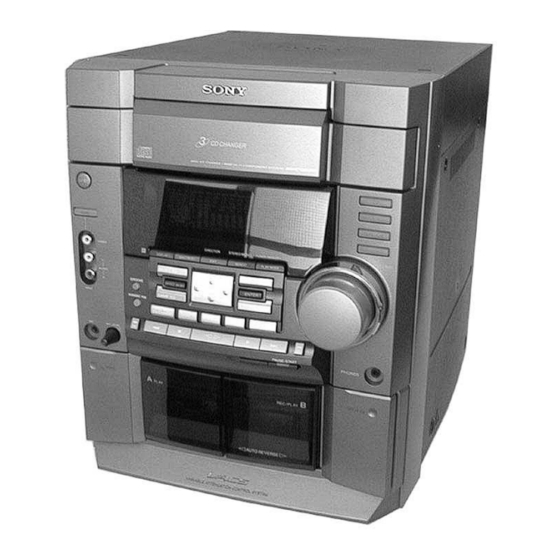
HCD-DX20/RG30
Photo: HCD-DX20
CD
Section
Tape deck
Section
SPECIFICATIONS
Model Name Using Similar Mechanism
CD Mechanism Type
Base Unit Name
Optical Pick-up Name
Model Name Using Similar Mechanism
SPEAKER:
accepts impedance of 6 to 16 ohms
CD player section
System
Compact disc and digital audio system
Laser
Semiconductor laser (λ=780 nm)
Emission duration: continuous
Laser output
Max. 44.6 µ W*
* This output is the value measured at a distance
of 200 mm from the objective lens surface on
the Optical Pick-up Block with 7 mm aper-
ture.
Frequency response
2 Hz – 20 kHz (±0.5 dB)
Wavelength
780 – 790 nm
Signal-to-noise ratio
More than 90 dB
Dynamic range
More than 90 dB
CD OPTICAL DIGITAL OUT
(Square optical connector jack, rear panel)
Wavelength
660 nm
Output Level
–18 dBm
MINI HIFI COMPONENT SYSTEM
AEP Model
UK Model
HCD-RG30
E Model
HCD-DX20
HCD-DX30/RG40
CDM58B-K6BD38
BU-K6BD38
KSM-213DAP
NEW
— Continued on next page —

Advertisement

Table of Contents
loading

Summary of Contents for Sony HCD-DX20

  • Page 1 HCD-DX20/RG30 SERVICE MANUAL AEP Model UK Model Ver 1.3 2003.12 HCD-RG30 E Model HCD-DX20 • HCD-DX20/RG30 is the tuner, deck, CD and amplifier section in MHC-DX20/RG30. Photo: HCD-DX20 Model Name Using Similar Mechanism HCD-DX30/RG40 CD Mechanism Type CDM58B-K6BD38 Section Base Unit Name...
  • Page 2 4-track 2-channel stereo BLOCK OR BASE UNIT Frequency response 40 – 13,000 Hz (±3 dB), using Sony TYPE I cassette The laser diode in the optical pick-up block may suffer electrostatic break-down because of the potential difference generated by the Tuner section charged electrostatic load, etc.
  • Page 3: Table Of Contents

    HCD-DX20/RG30 TABLE OF CONTENTS MODEL IDENTIFICATION — BACK PANEL — PARTS No. 1. SERVICE NOTE .............. 4 2. GENERAL ................. 5 3. DISASSEMBY ..............7 4. TEST MODE ..............13 5. ELECTRICAL ADJUSTMENTS ......17 6. DIAGRAMS 6-1. Circuit Board Location ............. 19 6-2.
  • Page 4: Service Note

    HCD-DX20/RG30 SECTION 1 Ver1.2 2003.01 SERVICE NOTE REMOVING THE PANEL BOARD AND THE KEY BOARD * The panel board and the key board only are connected to the front panel by means of hot-melting the plastics. 5 Key board 3 Panel board...
  • Page 5: General

    HCD-DX20/RG30 SECTION 2 GENERAL This section is extracted from instruction manual. Main unit 1 2 3 4 8 9 q; AUDIO jacks ed MD (VIDEO) qg BUTTON DESCRIPTIONS CD qs MIC jack* CD SYNC wf MIC LEVEL control* v/V/b/B 5...
  • Page 6: Remote Control

    HCD-DX20/RG30 Remote Control 1 2 3 4 CD qj MD (VIDEO) 9 BUTTON DESCRIPTIONS CLEAR 6 P FILE qd CLOCK/TIMER SELECT 2 PRESET EQ qg v/V/b/B qs CLOCK/TIMER SET 3 SLEEP 1 M (fast forward)/TUNING D.SKIP ql SURROUND 0 . (go back)/PRESET...
  • Page 7: Disassemby

    HCD-DX20/RG30 SECTION 3 DISASSEMBLY Note : Disassemble the unit in the order as shown below. Case (Side-R, Side-L, Top) CD door Front panel section Tape mechanism deck Panel board Key board CD mechanism deck Base unit, BD board (CDM58B) Driver board, Moter board, Address sensor board...
  • Page 8 HCD-DX20/RG30 3-2. CD DDOR CD door CD mechanism deck (CDM58B) 1 Turn the pulley to the direction of arrow. Front panel side pulley 2 Pull-out the disc tray. 3-3. FRONT PANEL SECTION 7 Connector (CN714) CD mechanism deck (CDM58B) 2 Connector...
  • Page 9 HCD-DX20/RG30 3-4. TAPE MECHANISM DECK 1 Six screws (+BVTP 2.6 × 8) 2 Tape mechanism deck 3-5. PANEL BOARD 6 Panel board 4 Connector (CN712) 2 Vol knob ring 5 Cut the seven melted-connection points with a cutting plier. 1 Volume knob Note: When attching the panel board, refer to "Service Note"...
  • Page 10 HCD-DX20/RG30 3-6. KEY BOARD 2 Key board 1 Cut the six melted-connection points with a cutting plier. Note: When attching the Key board, refer to "Service Note" on page 4. 3-7. SUB TRANS BOARD, VIDEO OUT BOARD, BACK PANEL, POWER TRANSFORMER (TRANS BOARD)
  • Page 11 HCD-DX20/RG30 3-8. MAIN BOARD, POWER AMP BOARD 7 Heat sink 6 Two screws (+BVTT 3 × 6) 4 Three screws (+BVTT 3 × 6) Main board 5 Power amp board 3 Two screws (+BVTP 3 × 16) 2 Main board 1 Two screws (+BVTT 3 ×...
  • Page 12 HCD-DX20/RG30 3-10. DRIVER BOARD, MOTOR BOARD AND ADDRESS SENSOR BOARD q; Screw (+PTPWH 2.6 × 8) 4 Two screws (+BVTP 2.6 × 8) 8 Motor board 6 Wire (flat type) 8p (CN721) 5 Remove the two solderings of motor. qs Screw (+BVTP 2.6 × 8)
  • Page 13: Test Mode

    HCD-DX20/RG30 SECTION 4 TEST MODE [MC Cold Reset] [Change-over of AM Tuner Step between 9 kHz and • The cold reset clears all data including preset data stored in the 10 kHz] RAM to initial conditions. Execute this mode when returning •...
  • Page 14 HCD-DX20/RG30 [MC Test Mode] [Microprocessor version display] • This mode is used to check operations of the respective sections • If the following operation is performed during the POWER OFF of Amplifier, TUNER, CD and Tape. in the modes other than the POWER SAVE mode (i.e., while the...
  • Page 15 HCD-DX20/RG30 [Aging Mode] This mode can be used for operation check of CD section and tape deck section. • If an error occurred: The aging operation stops and display status. • If no error occurs: The aging operation continues repeatedly.
  • Page 16 HCD-DX20/RG30 2) Operation during aging mode In the aging mode, the program is executed in the following sequence. (1) The disc tray opens and closes. (2) The mechanism accesses DISC 2 and makes an attempt to read TOC. However, since there are no discs, a message “CD2 NO DISC”...
  • Page 17: Electrical Adjustments

    HCD-DX20/RG30 SECTION 5 ELECTRICAL ADJUSTMENTS FM Tuned Level Adjustment CD SECTION FM RF Signalgenerator Note : 1. CD Block is basically designed to operate without adjustment. 75 Ω coaxial Therefore, check each item in order given. 2. Use YEDS-18 disc (3-702-101-01) unless otherwise indicated.
  • Page 18 HCD-DX20/RG30 Note : Clear RF signal waveform means that the shape “ ◊ ” can be clearly Adjustment Location: distinguished at the center of the waveform. [BD BOARD] (Conductor Side) RF signal waveform VOLT/DIV : 200mV TIME/DIV : 500ns level : 1.45 ± 0.3Vp-p...
  • Page 19: Diagrams

    HCD-DX20/RG30 SECTION 6 6-1. CIRCUIT BOARD LOCATION DIAGRAMS MOTOR board THIS NOTE IS COMMON FOR PRINTED WIRING BOARDS AND SCHEMATIC DIAGRAMS. (In addition to this, the necessary note is printed in each block.) ADDRESS SENSOR board VIDEO OUT board Note on Schematic Diagram: Note on Printed Wiring Boards: •...
  • Page 20: Block Diagrams Tuner Section

    HCD-DX20/RG30 6-2. BLOCK DIAGRAMS TUNER SECTION AM/FM FRONT-END, IFAMP, MPX DX20 IC101 TM101 FE101 Q101 CF101 CF102 RF IF L-CH • RCH is omitted ANT IN IF OUT FM IF L OUT Q103 • Signal Path FM 75 OSC OUT...
  • Page 21: Block Diagrams -Main Section

    HCD-DX20/RG30 MAIN SECTION RV703 IC702 IC702 (1/2) (2/2) LEVEL J702 MIC AMP IC501 JK302 L-CH TUNER TUNER L SECTION OUT L SPEAKER POWER IMPEDANCE Q361,362 Q381,382 USE 6-16Ω R CH LOUT MUTE MUTE CD L OUT R R CH SECTION...
  • Page 22: Printed Wiring Board -Bd Section

    HCD-DX20/RG30 6-3. PRINTED WIRING BOARD – BD SECTION – • See page 19 for Circuit Boards Location. • Semiconductor Location Ref. No. Location IC101 IC102 IC103 Q101 TP(TE0) (VC) TP(FE0) (RF) TP(FE1) TP(AGC CON) TP(D GND) (XPCK) CN102 (Page 24)
  • Page 23: Schematic Diagram -Bd Section

    HCD-DX20/RG30 6-4. SCHEMATIC DIAGRAM – BD SECTION – • See page 19 for Waveforms. • See page 40,41 for IC Block Diagrams. IC B/D IC B/D IC B/D (5/5) CN102 (Page 29)
  • Page 24: Printed Wiring Board -Main Section

    HCD-DX20/RG30 6-5. PRINTED WIRING BOARD – MAIN SECTION – • See page 19 for Circuit Boards Location. DRVER BOARD MAIN BOARD BOARD (Page 36) (Page 22) CLP2 • Semiconductor Location JW232 JR633 R119 Ref. No. Location JW004 R116 Ref. No. Location...
  • Page 25: Schematic Diagram -Main Section (1/5)

    HCD-DX20/RG30 6-6. SCHEMATIC DIAGRAM – MAIN SECTION (1/5) – • See page 42 for IC Block Diagrams.
  • Page 26: Schematic Diagram -Main Section (2/5)

    HCD-DX20/RG30 6-7. SCHEMATIC DIAGRAM – MAIN SECTION (2/5) – • See page 19 for Waveforms. • See page 41,42 for IC Block Diagrams.
  • Page 27: Schematic Diagram -Main Section (3/5)

    HCD-DX20/RG30 6-8. SCHEMATIC DIAGRAM – MAIN SECTION (3/5) –...
  • Page 28: Schematic Diagram -Main Section (4/5)

    HCD-DX20/RG30 6-9. SCHEMATIC DIAGRAM – MAIN SECTION (4/5) – • See page 19 for Waveforms. • See page 37 for IC Pin Function Description.
  • Page 29: Schematic Diagram -Main Section (5/5)

    HCD-DX20/RG30 6-10. SCHEMATIC DIAGRAM – MAIN SECTION (5/5) –...
  • Page 30: Printed Wiring Board -Power Amp Section

    HCD-DX20/RG30 6-11. PRINTED WIRING BOARD – POWER AMP SECTION – • See page 19 for Circuit Boards Location. POWER AMP BOARD (CHASSIS) RG30/DX20:KR • Semiconductor Location Ref. No. Location D501 D502 D541 D542 D543 D551 RG30/ IC501 R519 DX20:KR Q501...
  • Page 31: Schematic Diagram -Power Amp Section

    HCD-DX20/RG30 6-12. SCHEMATIC DIAGRAM – POWER AMP SECTION –...
  • Page 32: Printed Wiring Board -Panel Section

    HCD-DX20/RG30 6-13. PRINTED WIRING BOARD – PANEL SECTION – • See page 19 for Circuit Boards Location. PANEL BOARD • Semiconductor Location Ref. No. Location D701 D702 TUNER/BAND D703 D704 61 60 IC701 D705 D706 DX20 D707 D708 D709 D710...
  • Page 33: Schematic Diagram -Panel Section

    HCD-DX20/RG30 6-14. SCHEMATIC DIAGRAM – PANEL SECTION – • See page 19 for Waveforms. SEN701...
  • Page 34: Printed Wiring Board -Trans Section

    HCD-DX20/RG30 6-15. PRINTED WIRING BOARD – TRANS SECTION – • See page 19 for Circuit Boards Location. SUB TRANS BOARD DX20:AR,E2, E51,EA,SP • Semiconductor Location AC IN Ref. No. Location D901 D902 D903 D904 D905 RG30/DX20:KR, D911 MX,TH D912 D913...
  • Page 35: Schematic Diagram -Trans Section

    HCD-DX20/RG30 6-16. SCHEMATIC DIAGRAM – TRANS SECTION –...
  • Page 36: Printed Wiring Board -Driver Section

    HCD-DX20/RG30 6-17. PRINTED WIRING BOARD – DRIVER SECTION – • See page 19 for Circuit Boards Location. • Semiconductor Location Ref. No. Location D707 IC701 IC711 (Page 24 ) 6-18. SCHEMATIC DIAGRAM – DRIVER SECTION – • See page 42 for IC Block Diagrams.
  • Page 37: Ic Pin Function Description

    HCD-DX20/RG30 6-19. IC PIN FUNCTION DESCRIPTION • MAIN BOARD IC401 M30622MCA-B23FP (MASTER CONTROL) Pin No. Pin Name Description S-OUT Serial data output the display control. S-CLK Serial clock output from main controller. S-BSY Busy signal input from the display control. “L” : busy REMOTE IN Pemoto commander input.
  • Page 38 HCD-DX20/RG30 Pin No. Pin Name Description NO USE — Not used. CENT-MUTE — Not used. REAR-MUT — Not used. 494-DAT — Not used. 494-CLK — Not used. 494-LT — Not used. SUR1 — Not used. SUR2 — Not used. SUR3 —...
  • Page 39 HCD-DX20/RG30 • PANEL BOARD IC701 UPD780232GC-031-8BT (DISPLAY CONTROL) Pin No. Pin Name Description Power supply.(+5V) — Connected to ground. System clock output terminal.(5MHz) System clock input terminal.(5MHz) — Connected to ground. RESET Reset signal input from main controller. S-CLK Serial clock input from main controller.
  • Page 40: Ic Block Diagrams

    HCD-DX20/RG30 6-20. IC BLOCK DIAGRAMS IC101 CXD2587Q (BD BOARD) ERROR DIGITAL CORRECTOR DIGITAL ASYMMETRY CORRECTION OPERATIONAL LRCK AMPLIFIER ANALOG SWITCH PCMD INTERFACE DEMODULATOR CONVERTER EMPH XVDD XTAI TIMING LOGIC CLOCK XTAO XTSL GENERATOR XVSS TES1 AVDD1 TEST AOUT1 SERVO DSP...
  • Page 41 HCD-DX20/RG30 IC103 CXA2568M-T6 (BD BOARD) IC103 BU1924 (MAIN BOARD) APC PD AMP LC/PD LD_ON CLOCK HOLD TEST AGCVTH VREF APC LD AMP HOLD_SW AGCCONT DEFFERENTIAL BIPHASE PLL 57KHz (50%/30% DECODER DECODER 1187.5Hz RDS/ARI OFF) RF_BOT 8TH SWITCHED CAPACITOR FILTER RFTC...
  • Page 42 HCD-DX20/RG30 IC101 BA1450 (MAIN BOARD) AM IF VREG DECODER DRIVER COMP IC701 BA6956AN (DRIVER BOARD) IC201 TA8189N (MAIN BOARD) METAL TAPE A CH2/A CH2/B /TAPE B – – CONTROL LOGIC VREF1 IREF VREF2 – – CH1/A CH1/B METAL GND1...
  • Page 43: Exploded Views

    HCD-DX20/RG30 SECTION 7 EXPLODED VIEWS NOTE: The components identified by • Items marked “*” are not stocked since they are • Abbreviation mark 0 or dotted line with mark seldom required for routine service. Some delay : Saudi Arabia model 0 are critical for safety.
  • Page 44: Front Panel Section

    HCD-DX20/RG30 7-2. FRONT PANEL SECTION * For service only (Be sure to refer to "Service note" on page 4.) FLD1 not supplied not supplied Ref. No. Part No. Description Remark Ref. No. Part No. Description Remark 4-234-019-01 VOLUME KNOB (RG30)
  • Page 45: Chassis Section

    HCD-DX20/RG30 Ver1.1 2002.05 7-3. CHASSIS SECTION T911 not supplied not supplied Ref. No. Part No. Description Remark Ref. No. Part No. Description Remark 1-773-049-11 WIRE (FLAT TYPE)(17 CORE) 4-966-266-01 BUSHING (S) (FBS002), CORD (DX20:E2, MX) A-4476-781-A MAIN BOARD, COMPLETE (DX20:EA)
  • Page 46: Cd Mechanism Deck Section

    HCD-DX20/RG30 Ver 1.3 7-4. CD MECHANISM DECK SECTION M721 supplied supplied Ref. No. Part No. Description Remarks Ref. No. Part No. Description Remarks 4-933-134-11 SCREW (+PTPWH M2.6X8) X-4951-889-1 HOLDER (BU) ASSY 4-221-679-01 CAM (RELAY) 4-222-095-01 BELT 4-231-452-01 TABLE (NEW) 4-227-045-11 SPRING (INSULATOR), COIL 4-221-686-01 LEVER (CHANGE) 4-985-672-01 SCREW (+PTPWH M2.6), FLOATING...
  • Page 47: Electrical Parts List

    HCD-DX20/RG30 SECTION 8 ADDRESS SENSOR ELECTRICAL PARTS LIST Ref. No. Part No. Description Remarks Ref. No. Part No. Description Remarks Note: • SEMICONDUCTORS • Due to standardization, replacements in the parts The components identified by In each case, u: µ , for example:...
  • Page 48 HCD-DX20/RG30 DRIVER Ref. No. Part No. Description Remarks Ref. No. Part No. Description Remarks R111 1-216-121-11 RES-CHIP 1/10W < DIODE > R113 1-216-121-11 RES-CHIP 1/10W R114 1-216-073-00 RES-CHIP 1/10W D707 8-719-058-04 DIODE SEL5223S-TP15 (REC PAUSE/START) R116 1-216-001-00 METAL CHIP 1/10W...
  • Page 49 HCD-DX20/RG30 MAIN Ref. No. Part No. Description Remarks Ref. No. Part No. Description Remarks S712 1-762-875-21 SWITCH, KEYBOARD (KARAOKE PON) (DX20) C123 1-162-964-11 CERAMIC CHIP 0.001uF S713 1-762-875-21 SWITCH, KEYBOARD (m – ) C124 1-162-964-11 CERAMIC CHIP 0.001uF S714 1-762-875-21 SWITCH, KEYBOARD (.)
  • Page 50 HCD-DX20/RG30 MAIN Ref. No. Part No. Description Remarks Ref. No. Part No. Description Remarks C201 1-162-963-11 CERAMIC CHIP 680PF C241 1-130-479-00 MYLAR 0.0047uF 5% C202 1-162-963-11 CERAMIC CHIP 680PF C242 1-130-471-00 MYLAR 0.001uF C243 1-162-965-11 CERAMIC CHIP 0.0015uF 10% C203...
  • Page 51 HCD-DX20/RG30 MAIN Ref. No. Part No. Description Remarks Ref. No. Part No. Description Remarks C352 1-162-962-11 CERAMIC CHIP 470PF C685 1-126-768-11 ELECT 2200uF (DX20) C686 1-126-964-11 ELECT 10uF C356 1-126-963-11 ELECT 4.7uF C360 1-164-156-11 CERAMIC CHIP 0.1uF C687 1-126-916-11 ELECT 1000uF 6.3V...
  • Page 52 HCD-DX20/RG30 MAIN Ref. No. Part No. Description Remarks Ref. No. Part No. Description Remarks D684 8-719-083-89 DIODE 11ES2N-TB5 JR14 1-216-864-11 METAL CHIP 1/16W D685 8-719-988-61 DIODE 1SS355TE-17 (DX20) D686 8-719-988-61 DIODE 1SS355TE-17 JR15 1-216-864-11 METAL CHIP 1/16W D687 8-719-083-89 DIODE 11ES2N-TB5...
  • Page 53 HCD-DX20/RG30 MAIN Ref. No. Part No. Description Remarks Ref. No. Part No. Description Remarks Q222 8-729-119-78 TRANSISTOR 2SC2785-HFE R119 1-216-833-11 METAL CHIP 1/16W Q223 8-729-142-46 TRANSISTOR 2SC2001-LK R120 1-216-833-11 METAL CHIP 1/16W Q224 8-729-119-78 TRANSISTOR 2SC2785-HFE R121 1-216-821-11 METAL CHIP...
  • Page 54 HCD-DX20/RG30 MAIN Ref. No. Part No. Description Remarks Ref. No. Part No. Description Remarks R221 1-216-833-11 METAL CHIP 1/16W R304 1-216-838-11 METAL CHIP 1/16W R222 1-216-813-11 METAL CHIP 1/16W R305 1-216-825-11 METAL CHIP 2.2K 1/16W R223 1-216-848-11 METAL CHIP 180K...
  • Page 55 HCD-DX20/RG30 MAIN Ref. No. Part No. Description Remarks Ref. No. Part No. Description Remarks R381 1-216-842-11 METAL CHIP 1/16W R641 1-216-823-11 METAL CHIP 1.5K 1/16W (DX20) (DX20:KR,SP,TH) R382 1-216-842-11 METAL CHIP 1/16W (RG30) R641 1-216-837-11 METAL CHIP 1/16W R382 1-216-841-11 METAL CHIP...
  • Page 56 HCD-DX20/RG30 MOTOR PANEL Ref. No. Part No. Description Remarks Ref. No. Part No. Description Remarks 1-675-910-14 MOTOR BOARD C734 1-162-306-11 CERAMIC 0.01uF *********** C735 1-162-306-11 CERAMIC 0.01uF C736 1-162-294-31 CERAMIC 0.001uF < CAPACITOR > C737 1-162-294-31 CERAMIC 0.001uF C721 1-162-306-11 CERAMIC 0.01uF...
  • Page 57 HCD-DX20/RG30 PANEL POWER AMP Ref. No. Part No. Description Remarks Ref. No. Part No. Description Remarks < FERRITE BEAD > R768 1-247-807-31 CARBON 1/4W R769 1-249-401-11 CARBON 1/4W F FB701 1-412-473-21 INDUCTOR R770 1-249-417-11 CARBON 1/4W F (DX20) < FLUORESCENT INDICATOR>...
  • Page 58 HCD-DX20/RG30 SUB TRANS POWER AMP Ref. No. Part No. Description Remarks Ref. No. Part No. Description Remarks C507 1-130-493-00 MYLAR 0.068uF (DX20) C508 1-130-493-00 MYLAR 0.068uF R504 1-249-435-11 CARBON 1/4W C509 1-126-965-11 ELECT 22uF (RG30) C511 1-162-306-11 CERAMIC 0.01uF C512 1-162-294-31 CERAMIC 0.001uF...
  • Page 59 HCD-DX20/RG30 Ver 1.3 SUB TRANS TRANS VIDEO OUT Ref. No. Part No. Description Remarks Ref. No. Part No. Description Remarks < DIODE > R916 1-247-807-31 CARBON 1/4W D901 8-719-991-33 DIODE 1SS133T-77 0 R919 1-219-122-91 FUSIBLE 0.33 1/4W D902 8-719-200-82 DIODE 11ES2...
  • Page 60 HCD-DX20/RG30 REVISION HISTORY Clicking the version allows you to jump to the revised page. Also, clicking the version at the upper right on the revised page allows you to jump to the next revised page. Ver. Date Description of Revision 2001.06...

This manual is also suitable for:

Hcd-rg30

Table of Contents