Table of Contents
Advertisement
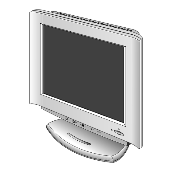
COLOR MONITOR
SERVICE MANUAL
CHASSIS NO. : CL-06
MODEL:
StudioWorks 570LE / 570LS, LB570BZ
ID LABEL : LB570D-EA / LB570E-EA / LB570D-EN
CAUTION
BEFORE SERVICING THE UNIT,
READ THE SAFETY PRECAUTIONS IN THIS MANUAL.
Website:http://biz.LGservice.com
E-mail:http://www.LGEservice.com/techsup.html
Same looking with New Chassis
Issue Date: JULY 2000
Advertisement
Table of Contents


Need help?
Do you have a question about the StudioWorks 570LE and is the answer not in the manual?
Questions and answers