Table of Contents
Advertisement
Quick Links
Download this manual
See also:
Instruction Manual
Advertisement
Table of Contents

Subscribe to Our Youtube Channel
Related Manuals for Icom IC-2800H


Summary of Contents for Icom IC-2800H
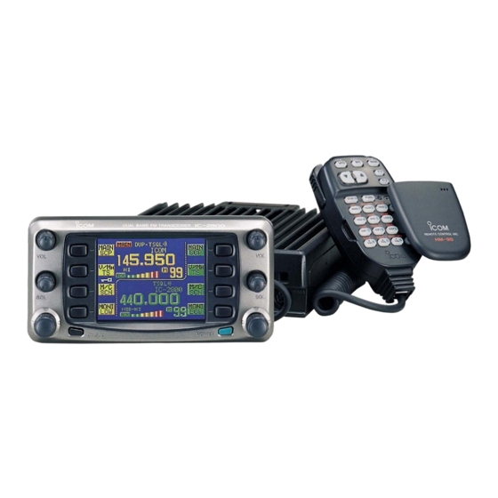
- Page 1 DUAL BAND FM TRANSCEIVER iC-2800h...
- Page 2 This service manual describes the latest service information for connect the transceiver to an AC outlet or to a DC the IC-2800H FM TRANSCEIVER at the time of publication. power supply that uses more than 16 V. Such a connection could cause a fire hazard and/or electric shock.
- Page 3 TABLE OF CONTENTS SECTION 1 SPECIFICATIONS SECTION 2 INSIDE VIEWS SECTION 3 DISASSEMBLY INSTRUCTIONS SECTION 4 CIRCUIT DESCRIPTION 4 - 1 RECEIVER CIRCUITS ....................4 – 1 4 - 2 TRANSMITTER CIRCUITS ................... 4 – 3 4 - 3 PLL CIRCUIT ........................4 – 4 4 - 4 POWER SUPPLY CIRCUITS ..................
- Page 4 SECTION 1 SPECIFICATIONS GENERAL • Frequency range Version 144 MHz band 440 MHz band 144.000 – 146.000 430.000 – 440.000 Rx: 136.000 – 174.000* Rx: 400.000 – 530.000* Tx: 144.000 – 148.000* Tx: 430.000 – 440.000* Rx: 118.000 – 174.000* 430.000 –...
-
Page 5: Control Unit
SECTION 2 INSIDE VIEWS • CONTROL UNIT * : Located underside of this point SUB CPU (IC10: HD6433032SK) CFL drive (Q14, Q15, Q19*, Q20*) CPU reset IC* (IC11: S-80945ANMP-DD9) LCD controller (IC8: SED1354F0A) R-data buffer amplifier* (Q13: 2SA1576) T-data buffer amplifier* (Q12: 2SC4081) •... - Page 6 SECTION 3 DISASSEMBLY INSTRUCTIONS • Removing the MAIN unit • Removing the CONTROL unit q Unscrew 1 screw, q Unscrew 4 screws, , and remove the cover. , and remove the cover. w Unplug J4 to separate the fan motor from the MAIN unit. w Unplug J5 to separate the speaker and front panel.
-
Page 7: Receiver Circuits
SECTION 4 CIRCUIT DESCRIPTION 4-1 RECEIVER CIRCUITS The tunable bandpass filters (D11–D13, D15) employ varac- tor diodes to tune the center frequency of the RF passband 4-1-1 DUPLEXER CIRCUIT for wide bandwidth receiving and good image response The transceiver has a duplexer (low-pass and high-pass fil- rejection. - Page 8 The 1st IF signal from the 2nd IF amplifier is applied to the 4-1-9 VHF SQUELCH CIRCUIT 2nd mixer section of IC28 (pin 16), and is mixed with a 15.2 • NOISE SQUELCH MHz 2nd LO signal generated by the reference oscillator cir- A noise squelch circuit cuts out AF signals when no RF sig- cuit (X1, IC2) to produce a 450 kHz VHF 2nd IF signal.
-
Page 9: Transmitter Circuits
4-1-10 UHF RF CIRCUIT 4-2 TRANSMITTER CIRCUITS The UHF RF signals are passed through part of a duplexer 4-2-1 MICROPHONE AMPLIFIER CIRCUIT (high-pass filter; L44, L45, L82, C189, C190, C493). The sig- The microphone amplifier circuit amplifies audio signals from nals are then passed through the low-pass filter (L42, L43, the microphone to a level needed at the modulation circuit. -
Page 10: Pll Circuits
4-2-5 VHF APC CIRCUIT 4-2-9 UHF APC CIRCUIT The APC circuit protects the power amplifier from a mis- The APC detector circuit (D25 and D26) detects forward sig- matched output load and stabilizes transmit output power. nals and refrection signals respectively. The combined volt- age is at a minimum level when the antenna is matched at 50 Ω... -
Page 11: Power Supply Circuits
4-3-3 UHF LOOP 4-4 POWER SUPPLY CIRCUITS The generated signal at the U-VCO (Q20, Q21, D20, D21) • VOLTAGE LINE enters the PLL IC (IC2, pin 15) via buffer-amplifiers (Q22, Line Description Q23) and is divided at the programmable divider section and is then applied to the phase detector section. -
Page 12: Port Allocations
4-5 PORT ALLOCATIONS 4-5-1 CPU (MAIN UNIT; IC19) Port Port Description Description number name number name Input port for the decoded CTCSS sig- Outputs transmit signal for VHF band. TONEIN nals. High : While transmitting on VHF band. OSC1, Input ports for the CPU system clock 7, 8 OSC2 oscillator (X4: 10.000 MHz). - Page 13 SECTION 5 ADJUSTMENT PROCEDURES 5-1 PREPARATION All adjustments in this section must be performed on wide bandwidth condition unless specified otherwise. (Narrow bandwidth is selectable for Europe and Italy vertions only.) ‘ ‘ REQUIRED TEST EQUIPMENT EQUIPMENT GRADE AND RANGE EQUIPMENT GRADE AND RANGE Output voltage...
-
Page 14: Pll And Transmitter Adjustments
5-2 PLL AND TRANSMITTER ADJUSTMENTS ADJUSTMENT MEASUREMENT POINT ADJUSTMENT ADJUSTMENT CONDITION VALUE UNIT LOCATION UNIT ADJUST PLL LOCK • VHF displayed freq. : MAIN Connect a digital 1.65 V MAIN VOLTAGE 145.000 MHz multi-meter or oscil- • Receiving loscope check point CP-LV. •... - Page 15 DC power supply 13.8 V / 20 A R119 R119 UHF output power VHF output power adjustment adjustment CP-LV PLL lock voltage check point Reference frequency adjustment PLL lock voltage adjustment VHF deviation adjustment UHF deviation adjustment Controller 5 - 3...
-
Page 16: Receiver Adjustments
5-3 RECEIVER ADJUSTMENTS The receiver adjustments must be performed after PLL ADJUSTMENTS. ADJUSTMENT ADJUSTMENT CONDITION OPERATION • Turn into sensitivity setting mode. • Connect a JIG1 to the [MIC] connector, then turn SENSITIVITY power ON. • Select an adjustment channel by pushing 1st or 2nd •... - Page 17 RECEIVER ADJUSTMENTS (continued) ADJUSTMENT MEASUREMENT POINT ADJUSTMENT ADJUSTMENT CONDITION VALUE UNIT LOCATION UNIT ADJUST SQUELCH • UHF displayed freq. : Speaker At the point where the MAIN R229 (UHF) 445.000 MHz [USA] signal just appears. 435.000 MHz other • Set the squelch level to 22 % using the HM-98 microphone.
- Page 18 SECTION 6 PARTS LIST [CONTROL UNIT] [CONTROL UNIT] ORDER ORDER DESCRIPTION DESCRIPTION 1130009250 S.IC MN83951 7030003520 S.RESISTOR ERJ3GEYJ 472 V (4.7 kΩ) 1130008560 S.IC TC75S51F (TE85L) 7030003520 S.RESISTOR ERJ3GEYJ 472 V (4.7 kΩ) ERJ3GEYJ 101 V (100 Ω) 1180001830 S.IC M5291FP 7030003320 S.RESISTOR ERJ3GEYJ 101 V (100 Ω)
- Page 19 [CONTROL UNIT] [CONTROL UNIT] ORDER ORDER DESCRIPTION DESCRIPTION R127 7030003440 S.RESISTOR ERJ3GEYJ 102 V (1 kΩ) R240 7030003560 S.RESISTOR ERJ3GEYJ 103 V (10 kΩ) ERJ3GEYJ 471 V (470 Ω) R128 7030003400 S.RESISTOR R241 7030003560 S.RESISTOR ERJ3GEYJ 103 V (10 kΩ) R129 7030003560 S.RESISTOR ERJ3GEYJ 103 V (10 kΩ)
- Page 20 [CONTROL UNIT] [CONTROL UNIT] ORDER ORDER DESCRIPTION DESCRIPTION 4030007090 S.CERAMIC C1608 CH 1H 470J-T-A C121 4310001070 MYLAR 100 SMC 333K 4030007090 S.CERAMIC C1608 CH 1H 470J-T-A C122 4030014540 S.CERAMIC GHM1038 SL 330J 3KV 4030007090 S.CERAMIC C1608 CH 1H 470J-T-A C123 4510006970 S.ELECTROLYTIC ECEV1CA330WR 4030007090 S.CERAMIC C1608 CH 1H 470J-T-A...
- Page 21 [CONTROL UNIT] [MAIN UNIT] ORDER ORDER DESCRIPTION DESCRIPTION 5030001660 LCD EDTCA22QB0 1150001970 IC M67746-01 5080000430 CFL HMB S 3 AIW 83N/AZ ASSY 1130009180 S.IC M64076AGP 600C 1110003690 S.IC M62354GP 75EC 1150001620 IC M57788MR/SC-1318 2260002560 S.SWITCH EVQ-PPX A25 1110002750 S.IC TA75S01F (TE85R) 2260002560 S.SWITCH EVQ-PPX A25 1140003830 S.IC...
- Page 22 [MAIN UNIT] [MAIN UNIT] ORDER ORDER DESCRIPTION DESCRIPTION 1530003230 S.TRANSISTOR 2SC5085-Y (TE85R) 1790001670 S.DIODE RB706F-40T106 1530002850 S.TRANSISTOR 2SC4116-BL (TE85R) 1750000510 S.DIODE UM9401F [EUR], [ITA] only 1750000550 S.DIODE 1SS355 TE-17 1590000430 S.TRANSISTOR DTC144EUA T106 1160000060 S.DIODE DAN202U T107 1560000840 S.FET 2SK1829 (TE85R) 1790000860 S.DIODE MA133 (TX) [EUR], [ITA] only...
- Page 23 [MAIN UNIT] [MAIN UNIT] ORDER ORDER DESCRIPTION DESCRIPTION 6170000230 COIL LW-25 7030009550 S.RESISTOR ERJ3EKF 1203 V (120 kΩ) ERJ3GEYJ 101 V (100 Ω) 6110001610 COIL LA-244 7030003320 S.RESISTOR ERJ3GEYJ 561 V (560 Ω) 6110002150 COIL LA-385 7030003410 S.RESISTOR ERJ3GEYJ 470 V (47 Ω) 6200002840 S.COIL NL 252018T-R22J 7030003280 S.RESISTOR...
- Page 24 [MAIN UNIT] [MAIN UNIT] ORDER ORDER DESCRIPTION DESCRIPTION ERJ3GEYJ 271 V (270 Ω) ERJ3GEYJ 101 V (100 Ω) R103 7030003370 S.RESISTOR R186 7030003320 S.RESISTOR ERJ3GEYJ 150 V (15 Ω) R104 7030003440 S.RESISTOR ERJ3GEYJ 102 V (1 kΩ) R187 7030003220 S.RESISTOR R105 7030003680 S.RESISTOR ERJ3GEYJ 104 V (100 kΩ)
- Page 25 [MAIN UNIT] [MAIN UNIT] ORDER ORDER DESCRIPTION DESCRIPTION R259 7030003440 S.RESISTOR ERJ3GEYJ 102 V (1 kΩ) R368 7030003640 S.RESISTOR ERJ3GEYJ 473 V (47 kΩ) R260 7030003560 S.RESISTOR ERJ3GEYJ 103 V (10 kΩ) R369 7030003600 S.RESISTOR ERJ3GEYJ 223 V (22 kΩ) ERJ3GEYJ 181 V (180 Ω) R261 7030003350 S.RESISTOR...
- Page 26 [MAIN UNIT] [MAIN UNIT] ORDER ORDER DESCRIPTION DESCRIPTION MCR50JZHJ 39 Ω (390) R458 7030003520 S.RESISTOR ERJ3GEYJ 472 V (4.7 kΩ) R541 7030001080 S.RESISTOR R459 7030003440 S.RESISTOR ERJ3GEYJ 102 V (1 kΩ) R542 7030003560 S.RESISTOR ERJ3GEYJ 103 V (10 kΩ) R460 7030003440 S.RESISTOR ERJ3GEYJ 102 V (1 kΩ) R543...
- Page 27 [MAIN UNIT] [MAIN UNIT] ORDER ORDER DESCRIPTION DESCRIPTION 4030006860 S.CERAMIC C1608 JB 1H 102K-T-A C161 4030006860 S.CERAMIC C1608 JB 1H 102K-T-A 4550000530 S.TANTALUM TESVA 1V 104M1-8L C162 4030006980 S.CERAMIC C1608 CH 1H 070D-T-A 4550000510 S.TANTALUM TESVA 1V 473M1-8L C163 4030006860 S.CERAMIC C1608 JB 1H 102K-T-A 4550000550 S.TANTALUM TESVA 1V 224M1-8L...
- Page 28 [MAIN UNIT] [MAIN UNIT] ORDER ORDER DESCRIPTION DESCRIPTION C246 4030006860 S.CERAMIC C1608 JB 1H 102K-T-A C323 4030006860 S.CERAMIC C1608 JB 1H 102K-T-A C247 4030006860 S.CERAMIC C1608 JB 1H 102K-T-A C324 4030006860 S.CERAMIC C1608 JB 1H 102K-T-A C248 4030006860 S.CERAMIC C1608 JB 1H 102K-T-A C325 4030006860 S.CERAMIC C1608 JB 1H 102K-T-A...
- Page 29 [MAIN UNIT] [MAIN UNIT] ORDER ORDER DESCRIPTION DESCRIPTION C406 4030006900 S.CERAMIC C1608 JB 1E 103K-T-A C500 4030006860 S.CERAMIC C1608 JB 1H 102K-T-A C407 4030008860 S.CERAMIC C1608 JB 1C 153K-T-A C501 4030006860 S.CERAMIC C1608 JB 1H 102K-T-A C408 4030006860 S.CERAMIC C1608 JB 1H 102K-T-A C502 4030006860 S.CERAMIC C1608 JB 1H 102K-T-A...
- Page 30 SECTION 7 MECHANICAL PARTS AND DISASSEMBLY [CHASSIS PARTS] [MAIN UNIT] ORDER ORDER QTY. REF NO. DESCRIPTION REF NO. DESCRIPTION QTY. 6510004880 Antenna connector MR-DS-E 01 8900004880 Cable OPC-465 MF 1 2710000590 Fan motor MF40D-12H-001 8510010880 1642 VCO case 8930037120 1647 M-holder 8010017670 2047 Chassis 8930045960 2088 Spacer 8810008660 Screw PH BT M3...
- Page 31 MP19 (CO) MP7 (CO) MP10 (CO) MP30 (CO) SP1 (CO) MP10 (C) MP2 (C) J1 (C) MP21 (CO) MP19 (CO) MP11 (C) MP17 (CO) MP12 (C) CONTROL unit MP20 (CO) MP23 (CO) MP9 (C) WS1 (CO) MP17 (CO) MF1 (C) MP24 (CO) MP25 (CO) DS2 (CO)
- Page 32 SECTION SECTION 8 PARTS LIST SEMI-CONDUCTOR INFORMATION 8 - 1 TRANSISTORS 8 - 2 DIODES NAME SYMBOL INSIDE VIEW NAME SYMBOL INSIDE VIEW NAME SYMBOL INSIDE VIEW NAME SYMBOL INSIDE VIEW 1SS355 2SA1362-GR DA114 2SJ144-GR MA728 2SA1576A R 2SB1201-S DA115 1SS254 yellow 3SK166A-2-T7...
- Page 33 SECTION 9 BOARD LAYOUTS 9 - 1 CONTROL UNIT • TOP VIEW The combination of this page and the next page shows the unit layout in the same configuration as the actual from CFL BACK LIGHT P.C. Board. MP24 UVOL VVOL CFL+ NC NC CFL–...
- Page 34 CONTROL UNIT • BOTTOM VIEW The combination of this page and the previous page from SPEAKER (SP1) shows the unit layout in the same configuration as the actual P.C. Board. VVOL R145 R151 UVOL R151 R145 from CFL BACK LIGHT (DS2) EXT.
- Page 35 HV IN CLONE I/O EXT SP ANTENNA MAIN UNIT • TOP VIEW The combination of this page and the next page shows the unit layout in the same configuration as the actual P.C. Board. from FAN MOTOR FV 1 to OPTIONAL UNIT AFOUT PSQL MDATA E MIC MICE PTT EXTMIC MU/D M8V...
- Page 36 from EXT SP CLONE I/O MAIN UNIT • BOTTOM VIEW The combination of this page and the previous page shows the unit layout in the same configuration as the actual P.C. Board. AFOUT PSQL M8V MU/D EXTMIC PTT MICE MIC E MDATA RDATA TDATA PTTP...
- Page 37 INPUT POWER DC 13.8 V SECTION 10 BLOCK DIAGRAM — POWER SW CTRL 8V REG Q74 DTC143XU IC14 TA7808F Q75 2SB1201 FAN CONTROL 13.8V 2SC4081 2SB1132 MA8075 MF1 (CHASSIS) VR8V VT8V —15V 13.8V BACK LIGHT +5VA V BIAS SEL VT8V REG DC-DC Q34 UMG9N 1/2 Q9 2SC4081...
- Page 38 V_MOD MUT PROTECTER POWER SW CTRL Q2 2SC4213 8V REG Q74 DTC143XU D45 DSA3A1 IC14 TA7808F D46 RD20E Q75 2SB1201 13.8V V_SHIFT Q3 DTC144EU D2 MA77 PLL5V VR8V VT8V VVCO8V V BIAS SEL VT8V REG V_VCOS REG PLL5V Q34 UMG9N 1/2 Q1 2SC4081 Q9 2SC4081 Q13 DTC144EU...
- Page 39 V_VCO FREQ. TX/RX FREQ. [EUR] [ ITA] [USA] [SEA], [CSA] [EUR] [ITA] [USA] [SEA] [CSA] RX 128.35—130.35 MHz RX 120.35—158.35 MHz RX/TX 144—146 MHz RX/TX 136—174 MHz 118—174 MHz 136—174 MHz 118—174 MHz RX 120.35—158.35 MHz RX 120.35 —158.35 MHz V_VCO V_MOD MUTE BUFF AMP...
- Page 40 INPUT POWER V_VCO FREQ. DC 13.8 V TX/RX FREQ. [EUR] [ ITA] [USA] [SEA], [CSA] [EUR] [ITA] [USA] [SEA] [CSA] SECTION 10 BLOCK DIAGRAM RX 128.35—130.35 MHz RX 120.35—158.35 MHz RX 120.35—158.35 MHz RX 120.35 —158.35 MHz RX/TX 144—146 MHz RX/TX 136—174 MHz 118—174 MHz 136—174 MHz...
- Page 41 SECTION 11 VOLTAGE DIAGRAM CONTROL UNIT R285 10k R287 R288 R286 R112 10 H DS1 EDTCA22QB0 10 H 10 H 10 H 10 H R3 100 STH1 270p R4 100 R5 100 IC7 TC7W14FU CPH1 R6 100 CPH2 R7 100 CPH3 R8 100 INT/EXT...
- Page 42 R284 3.15 MA8033 L IC17 TA7 5.16 R112 10 H 10 H 560p R3 100 1SV282 270p R4 100 R5 100 IC7 TC7W14FU R6 100 C129 C149 R7 100 0.001 R8 100 0.001 1.71 10 H 1SS355 INT/EXT 4.7k HPOS1 5.11 IC23 TA78 5.13...
- Page 43 EXT V VIDEO DS2 HMBS 3 A1W 83N/AZ Assy CFL+ CFL— 13.06 12.6 IC17 TA78L05F 5.22 5.16 R297 DTC144EU 2SA1362 GR SLF6028T-101MR42 C164 12.08 C169 5.11 10 H 678XN-1369 2SB1132 R R294 12.46 IC14 TA78L05F 220p 6.56 220p 2.7k R165 R293 2SB798 DK 8.2k...
- Page 44 SECTION 11 VOLTAGE DIAGRAM EXT V VIDEO DS2 HMBS 3 A1W 83N/AZ Assy CONTROL UNIT CFL+ R285 10k R284 3.15 R287 CFL– 13.06 R288 R286 MA8033 L IC17 TA78L05F 12.6 5.16 5.22 DTC144EU 2SA1362 GR SLF6028T-101MR42 R297 R112 12.08 C164 10 H 10 H C169...
- Page 45 CLONE MAIN UNIT 4.7k VSHIFT 1SS355 4.96 4.96 0.042 PTTP R276 100k R273 0.042 R513 R300 1k LIMIT 100k R514 0.001 2.2k R471 1k 1SS355 100k 1SS355 2.2k R284 1k TONEIN VMMUTE R473 1k VSQL R274 R515 R474 1k VSOUT R475 1k USQL DATA...
- Page 46 CLONE Q1 2SC4081 Q3 DTC144EU D2 MA77 R18 100 4.7k 0.001 0.001 0.001 0.001 0.001 0.001 VSHIFT 1SS355 2SC4213 0.22 H 100p L2 LB-270 120k C485 0.3p C19 1p 0.82 H VV 0.6 VV 2.2 100k HVU350 0.001 2SC5085 0.001 2SC5085 2.7k 2SC5085...
- Page 47 U = 430 MHz Band VMH 6.21 VT 0.9 VT 8.2 VHL 6.11 V = 144 MHz Band 2SC3357 2SC2954 2SA1362 0.001 0.001 None = COMMON 2SC4081 CHASSIS VT 2.1 UNIT VT 6.9 IC1 M67746-01 R18 100 2.2k 0.001 0.001 0.001 4.7k 0.001...
- Page 48 CLONE U = 430 MHz Band VT 0.9 VMH 6.21 VT 8.2 VHL 6.11 V = 144 MHz Band 2SA1362 2SC3357 2SC2954 MAIN UNIT 0.001 0.001 Q1 2SC4081 None = COMMON 2SC4081 CHASSIS VT 2.1 VT 6.9 UNIT Q3 DTC144EU D2 MA77 R18 100 2.2k...
- Page 49 08190 Sant Cugat del Valles Barcelona, SPAIN Phone : ( 93 ) 590 26 70 Fax : ( 93 ) 589 04 46 A Division of Icom America Inc. 3071 #5 Road, Unit 9, Richmond, B.C., V6X 2T4, Canada : http://www.icomspain.com...
- Page 50 A-5570MI-S 6-9-16, Kamihigashi, Hirano-ku, Osaka 547-0002, Japan © 1999 by Icom Inc.
Need help?
Do you have a question about the IC-2800H and is the answer not in the manual?
Questions and answers