Sony ICD-UX71 Service Manual

Sony ICD-UX71 Service Manual

Ic recorder
Hide thumbs Also See for ICD-UX71:

Advertisement

SERVICE MANUAL
Ver. 1.0 2008.10
IC recorder section
Capacity (User available capacity)
ICD-UX71/UX71F:
1 GB (approx. 986 MB =1,034,354,688 Byte)
ICD-UX81/UX81F:
2 GB (approx. 1.92 GB =2,072,313,856 Byte)
ICD-UX91F:
4 GB (approx. 3.86 GB =4,147,806,208 Byte)
A part of the memory capacity is used as a
management area.
Recording time*
1
ICD-UX71/UX71F
ST mode
STSP mode
STLP mode
11 hr. 55 min. 17 hr. 55 min. 47 hr. 50 min.
SP mode
LP mode
71 hr. 45 min. 287 hr. 15 min.
ICD-UX81/UX81F
ST mode
STSP mode
STLP mode
23 hr. 55 min. 35 hr. 55 min. 95 hr. 55 min.
SP mode
LP mode
143 hr. 50 min. 575 hr. 35 min.
ICD-UX91F
ST mode
STSP mode
STLP mode
47 hr. 55 min. 72 hr.
192 hr.
SP mode
LP mode
288 hr.
1152 hr. 5 min.
(hr. : hours/min. : minutes)
1
*
When you are going to record continuously
for a long time, you may have to replace
the battery with a new one in the midst of
recording.
Sony Corporation
9-889-311-01
2008J04-1
Audio&Video Business Group
©
2008.10
Published by Sony Techno Create Corporation
ICD-UX71/UX71F/UX81/
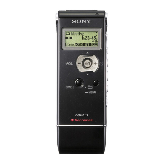
Photo: ICD-UX71
SPECIFICATIONS
Frequency range
ST : 40 Hz - 20,000 Hz
z
STSP : 40 Hz - 15,000 Hz
z
STLP : 60 Hz - 7,500 Hz
z
SP : 60 Hz - 10,000 Hz
z
LP : 60 Hz - 3,400 Hz
z
Bit rates and sampling frequencies for
MP3 fi les*
2
Bit rate: 32 - 320 kbps, VBR
Sampling frequencies: 16/22.05/24/32/44.1/
48 kHz
2
*
The playback of MP3 fi les recorded using the
IC recorder is also supported.
Not all encoders are supported.
Bit rate and sampling frequencies*
WMA fi les
Bit rate: 32 - 192 kbps*
4
, VBR
Sampling frequencies: 44.1 kHz
*
3
WMA Ver. 8 Class2A is compatible, however,
MBR (Multi Bit Rate), Lossless, Professional,
and Voice are not supported.
*
4
The NoiseSubstitution function is not
supported, therefore, playback becomes
simple playback with 32 kbps bit rate.
FM radio section
Frequency range
87.5 - 108 MHz
IF 150 kHz
Antenna
Headphone cord antenna
UX81F/UX91F
AEP Model
ICD-UX71/UX71F/UX81/UX81F
Chinese Model
ICD-UX71F/UX81F/UX91F
Latin American Model
ICD-UX71/UX71F/UX81/UX81F
General
Speaker
Approx. 10 mm dia.
Power output
90 mW
Input/Output
Microphone jack (minijack, stereo)
z
– input for plug in power, minimum input
level 0.9 mV, 3 kilohms or lower impedance
microphone
Headphone jack (minijack, stereo)
z
– output for 8 - 300 ohms headphones
USB connector
z
– High-Speed USB compatible
for
3
Playback speed control (DPC)
+100% to –50% (MP3)
0% to –50% (WMA)
Power requirements
One NH-AAA rechargeable battery (supplied):
1.2 V DC
One LR03 (size AAA) alkaline battery (not
supplied): 1.5 V DC
Operating temperature
5˚C - 35˚C
– Continued on next page –
IC RECORDER
E Model

Advertisement

Table of Contents
loading

Summary of Contents for Sony ICD-UX71

  • Page 1 Headphone cord antenna for a long time, you may have to replace the battery with a new one in the midst of recording. IC RECORDER Sony Corporation 9-889-311-01 2008J04-1 Audio&Video Business Group © 2008.10 Published by Sony Techno Create Corporation...
  • Page 2 ICD-UX71/UX71F/UX81/UX81F/UX91F Dimensions (w/h/d) (not incl. NOTES ON CHIP COMPONENT REPLACEMENT projecting parts and controls) (JEITA)* • Never reuse a disconnected chip component. 34.4 × 99.0 × 13.4 mm • Notice that the minus side of a tantalum capacitor may be dam- aged by heat.
  • Page 3: Table Of Contents

    ICD-UX71/UX71F/UX81/UX81F/UX91F TABLE OF CONTENTS GENERAL ..............DISASSEMBLY 2-1. Cover (USB) ..............2-2. Case Assy ................ 2-3. Audio Board Assy ............2-4. Main Board Assy ............TEST MODE ............DIAGRAMS 4-1. Block Diagram –Main Section– ........11 4-2. Block Diagram –Power/Display Section– ...... 12 4-3.
  • Page 4: General

    ICD-UX71/UX71F/UX81/UX81F/UX91F SECTION 1 GENERAL This section is extracted from instruction manual. How to use the control button Rear Operation indicator (17, 23, 24, 32, 39, Index to Parts and Press VOL – or + on the button to adjust 70, 74, 107) the volume.
  • Page 5 ICD-UX71/UX71F/UX81/UX81F/UX91F Display when listening to the FM Remaining battery/Charging radio indicator (for ICD-UX71F/UX81F/UX91F When a dry battery is used, the only) indicator shows the remaining battery power. While charging the rechargeable battery an animation appears. Remaining recording time indication Displays the remaining recording time in hours, minutes, and seconds.
  • Page 6: Disassembly

    ICD-UX71/UX71F/UX81/UX81F/UX91F SECTION 2 DISASSEMBLY • This set can be disassembled in the order shown below. 2-1. COVER (USB) (Page 6) 2-2. CASE ASSY (Page 7) 2-3. AUDIO BOARD ASSY (Page 8) 2-4. MAIN BOARD ASSY (Page 8) Note: Follow the disassembly procedure in the numerical order given.
  • Page 7: Case Assy

    ICD-UX71/UX71F/UX81/UX81F/UX91F 2-2. CASE ASSY screw (1.4) Unfasten the left claw of the LCD side while pressing the case assy. claw case assy claw claw Unfastened state. Unfasten the right claw of the LCD side with a supporting point by the MENU button.
  • Page 8: Audio Board Assy

    ICD-UX71/UX71F/UX81/UX81F/UX91F 2-3. AUDIO BOARD ASSY blue orange AUDIO board assy black battery terminal (–) screw (M 1.4) Remove the two solders. battery terminal (+) Remove the solder. CN8002 2-4. MAIN BOARD ASSY two screws (tapping (B 1.4) ) ornamental strip (AS) assy screw (B 1.4 )
  • Page 9: Test Mode

    R channel level is equal to the L channel level. RU: Russian and TH: Thai) * Make a mental note of the setting even when the battery has been (ICD-UX91 (4GB), ICD-UX81 (2GB), ICD-UX71 (1GB)) removed. Charge: C (With), No display (Without)
  • Page 10 ICD-UX71/UX71F/UX81/UX81F/UX91F 5. Beep 11. MENU INIT Test to Beep. Initialize the set values. LCD display [PLAY]: 800 Hz t 1.3 kHz t 2.0 kHz t 800 Hz ..[STOP]: STOP <Menu lnit> [PLAY]: ENTER 6. LCD Cont Adjust the LCD contrast.
  • Page 11: Diagrams

    ICD-UX71/UX71F/UX81/UX81F/UX91F SECTION 4 DIAGRAMS 4-1. BLOCK DIAGRAM – MAIN Section – SYSTEM CONTROL, D/A CONVERTER IC5001 (1/2) HP INSERT MIC INSERT EXTINT5(P26) EXTINT4(P25) STEREO CODEC,MIC/HP AMP IC1001 J1002 LIN2/IN2+ SDTO LIN2/IN2- SDTI DOUT UX71/UX81 R1044 R1062 BICK LOUT J1001 ROUT...
  • Page 12: Block Diagram -Power/Display Section

    ICD-UX71/UX71F/UX81/UX81F/UX91F 4-2. BLOCK DIAGRAM – POWER/DISPLAY Section – LCD CS NCS2(P20) LCD901 REAL TIME CLOCK LCD A0 EXA21(P2E) LIQUID IC3000 LCD RESET CRYSTAL XFCE2(P06) CPU VDD+3.1V DISPLAY CPU VDD+3.1V PANEL • Abbreviation LA : Latin American model SCK0 SCK0 SCK0...
  • Page 13 ICD-UX71/UX71F/UX81/UX81F/UX91F THIS NOTE IS COMMON FOR PRINTED WIRING BOARDS AND SCHEMATIC DIAGRAMS. (In addition to this, the necessary note is printed in each block.) For Printed Wiring Boards. For Schematic Diagrams. Note: Note: • All capacitors are in μF unless otherwise noted. (p: pF) 50 •...
  • Page 14: Printed Wiring Board -Audio Section

    ICD-UX71/UX71F/UX81/UX81F/UX91F 4-3. PRINTED WIRING BOARD – AUDIO Section – • : Uses unleaded solder. S4001 AUDIO BOARD MENU (SIDE A) • Semiconductor R2009 C2050 C2031 C2029 Q2007 R2017 Location JL2010 Q4002 C4015 C2011 C2014 Q4004 R4004 R2016 JL2000 R4008 S4001 Ref.
  • Page 15: Schematic Diagram -Audio Section (1/3)

    ICD-UX71/UX71F/UX81/UX81F/UX91F 4-4. SCHEMATIC DIAGRAM – AUDIO Section (1/3) – • See page 22 for IC Block Diagrams. • See page 25 for IC Pin Function Description of IC1001. AUDIO BOARD (1/3) AUDIO BOARD VDD_SPAMP (2/3) (Page 16) IC B/D R1062,1063...
  • Page 16: Schematic Diagram -Audio Section (2/3)

    ICD-UX71/UX71F/UX81/UX81F/UX91F 4-5. SCHEMATIC DIAGRAM – AUDIO Section (2/3) – • See page 22 for IC Block Diagrams. AUDIO BOARD (2/3) IC B/D IC2004 DC/DC CONVERTER IC2004 Q2007 LTC3526LEDC JL2005 L2001 JL2002 VOLTAGE DETECTOR 4.7uH DRY BATTERY VOUT VCC_3.3 SIZE"AAA" R2038...
  • Page 17: Schematic Diagram -Audio Section (3/3)

    ICD-UX71/UX71F/UX81/UX81F/UX91F 4-6. SCHEMATIC DIAGRAM – AUDIO Section (3/3) – • See page 24 for IC Block Diagram. AUDIO BOARD (3/3) CN4001 AUDIO UNREG_2.4 BOARD DGND DGND (2/3) CPU_VDD_3.1 DGND (Page 16) R4004 R4008 AUDIO_POWER_ON 2200 HOLD D4004,4005 DOUT DOUT (LCD BACK LIGHT)
  • Page 18: Printed Wiring Board -Main Section

    ICD-UX71/UX71F/UX81/UX81F/UX91F 4-7. PRINTED WIRING BOARD – MAIN Section – • : Uses unleaded solder. MAIN BOARD (SIDE A) CN8002 JL5025 RB7003 RB7002 RB7001 C5016 C5025 RB5001 C5004 D8002 D8001 LF8001 CN8001 (USB) IC7000 IC5001 *CSP (Chip Size Package) R5048 R7011...
  • Page 19: Schematic Diagram -Main Section (1/3)

    ICD-UX71/UX71F/UX81/UX81F/UX91F When IC5001 on the Main board is damaged, exchange the new Main board for the Main board which IC damaged. 4-8. SCHEMATIC DIAGRAM – MAIN Section (1/3) – • See page 24 for IC Block Diagram. • See page 26 for IC Pin Function Description of IC5001.
  • Page 20: Schematic Diagram -Main Section (2/3)

    ICD-UX71/UX71F/UX81/UX81F/UX91F When IC6000 and IC7000 on the Main board are damaged, exchange the new Main board for the Main board which IC damaged. 4-9. SCHEMATIC DIAGRAM – MAIN Section (2/3) – MAIN BOARD (2/3) CPU_VDD_3.1 R6002 MAIN BOARD (1/3) R6003...
  • Page 21: Schematic Diagram -Main Section (3/3)

    ICD-UX71/UX71F/UX81/UX81F/UX91F 4-10. SCHEMATIC DIAGRAM – MAIN Section (3/3) – MAIN BOARD (3/3) CN8002 DGND DGND DGND AUDIO_POWER_ON AUDIO_POWER_ON HOLD DOUT DOUT SP/HP_SEL SP/HP_SEL DAMP_SEL DAMP_SEL SP_SHDN SP_SHDN LRCK LRCK MUTE MUTE VCC_3.3 DATA DATA DX/LO DX/LO SDI1 SDI1 SCK1 SCK1...
  • Page 22 ICD-UX71/UX71F/UX81/UX81F/UX91F • IC Block Diagrams IC1002 LV24230LS-TLM-E (AUDIO Board (1/3)) IC2002 TK77335AM4 (AUDIO Board (2/3)) NC 1 8 NC VOUT VOLTAGE LINE OUT L STABILIZER PGND LINE SW BUFFER EACH BLOCK VREF MUTE PGND PGND ON/OFF STEREO CONTROL 6 NC...
  • Page 23 ICD-UX71/UX71F/UX81/UX81F/UX91F IC2003 XC9128D45CDR (AUDIO Board (2/3)) PGND PHASE CURRENT SENSE, VOUT COMPENATION LIMIT,PFM ERROR COMPARATOR PWM/PFM BUFFER CONTROLLER/LOGIC DRIVER RAMP WAVE MODE MODE GENERATOR VREF WITH SOFT START THERMAL SHUTDOWN 8 FB 7 AGND CURRENT LIMIT, THERMAL, 6 AEN SOFT START,...
  • Page 24 ICD-UX71/UX71F/UX81/UX81F/UX91F IC2013 NJM2746RB1(TE2) (AUDIO Board (2/3)) AOUT A–IN BOUT A+IN B–IN B+IN IC3000 RTC-4574NB (AUDIO Board (3/3)) 32.768kHz CONTROL LINE DIVIDER CLOCK and CALENDAR OUTPUT FCON TIMER REGISTER CONTROLLER 22 NC INTERRUPTS ALARM REGISTER CONTROLLER CONTROL REGISTER DATA INTERFACE CIRCUIT...
  • Page 25 ICD-UX71/UX71F/UX81/UX81F/UX91F • IC Pin Function Description AUDIO BOARD IC1001 AK4645EZ-L (STEREO CODEC, MIC/HP AMP) Pin No. Pin Name Description MPWR Power supply pin for microphone VCOM Common voltage output Bias voltage of ADC output and DAC output AVSS — Analog ground pin AVDD —...
  • Page 26 ICD-UX71/UX71F/UX81/UX81F/UX91F MAIN BOARD IC5001 LC823403B-08B-E (SYSTEM CONTROL, D/A CONVERTER) Pin No. Pin Name Description TEST1 Test pin 1 TEST2 Test pin 2 TEST3 Test pin 3 TEST4 Test pin 4 TEST5 Test pin 5 TEST6 Test pin 6 JTAG test clock signal input...
  • Page 27 ICD-UX71/UX71F/UX81/UX81F/UX91F Pin No. Pin Name Description SCK1(P14) Serial interface 1 clock signal output ADDA serial clock signal output SDO1(P15) Serial interface 1 data signal output ADDA serial data signal output SDI1(P16) Serial interface 1 data signal input ADDA serial data signal input...
  • Page 28 ICD-UX71/UX71F/UX81/UX81F/UX91F Pin No. Pin Name Description SDAT3 SD card data bit 2 signal input/output Connected to ground in this set. SDAT4 SD card data bit 3 signal input/output Connected to ground in this set. VDDRTC — Digital power supply pin (+1.0V) VSSRTC —...
  • Page 29 ICD-UX71/UX71F/UX81/UX81F/UX91F Pin No. Pin Name Description AVDDPLL1 — PLL1 analog power supply pin (+1.0V) AVSSPLL1 — PLL1 analog ground pin VCNT1 PLL1 VCO control signal output VDDXT — System/USB PHY oscillation amplifi er power supply pin (+1.0V) VSSXT — System/USB PHY oscillation amplifi er ground pin XIN1 System/USB PHY oscillation amplifi...
  • Page 30 ICD-UX71/UX71F/UX81/UX81F/UX91F Pin No. Pin Name Description @Crip — Not used. (Open) @Crip — Not used. (Open) @Crip — Not used. (Open) @Crip — Not used. (Open) @Crip — Not used. (Open) @Crip — Not used. (Open) @Crip — Not used. (Open) @Crip —...
  • Page 31: Exploded Views

    ICD-UX71/UX71F/UX81/UX81F/UX91F SECTION 5 EXPLODED VIEWS Note: • -XX and -X mean standardized parts, so • Color Indication of Appearance Parts Ex- they may have some difference from the ample: original one. KNOB, BALANCE (WHITE) . . . (RED) ↑ ↑...
  • Page 32: Main Board Section

    ICD-UX71/UX71F/UX81/UX81F/UX91F 5-2. MAIN BOARD SECTION AUDIO board section not supplied not supplied case rear section Ref. No. Part No. Description Remark Ref. No. Part No. Description Remark 3-234-449-11 SCREW (M1.4) X-2342-836-1 MAIN BOARD, COMPLETE (for SERVICE) 3-270-025-01 TERMINAL (+), BATTERY (EXCEPT LA)
  • Page 33: Case Rear Section

    ICD-UX71/UX71F/UX81/UX81F/UX91F 5-3. CASE REAR SECTION SP901 not supplied Ref. No. Part No. Description Remark Ref. No. Part No. Description Remark A-1565-721-A CASE (RWC9) SUB ASSY (WHITE)...(WHITE) A-1567-304-A CASE (RSE7) SUB ASSY (SILVER)...(SILVER) (UX91F:CH) (UX71F:E,KR,LA) A-1565-731-A CASE (RSC8) SUB ASSY (SILVER)...(SILVER) A-1567-317-A CASE (RB77) SUB ASSY (BLACK)...(BLACK)
  • Page 34: Audio Board Section

    ICD-UX71/UX71F/UX81/UX81F/UX91F 5-4. AUDIO BOARD SECTION LCD901 MIC902 MIC903 J1001 J1002 not supplied not supplied Ref. No. Part No. Description Remark Ref. No. Part No. Description Remark 3-270-003-01 CUSHION (LCD) A-1567-613-A AUDIO BOARD, COMPLETE 3-286-614-01 SHEET, ADHESIVE (UX71F:LA/UX81F:LA) 3-270-005-01 SHEET (LIGHT GUIDE PLATE) 3-234-449-11 SCREW (M1.4)
  • Page 35: Electrical Parts List

    ICD-UX71/UX71F/UX81/UX81F/UX91F SECTION 6 AUDIO ELECTRICAL PARTS LIST Note: • Due to standardization, replacements in • RESISTORS When indicating parts by reference num- the parts list may be different from the All resistors are in ohms. ber, please include the board name.
  • Page 36 ICD-UX71/UX71F/UX81/UX81F/UX91F AUDIO Ref. No. Part No. Description Remark Ref. No. Part No. Description Remark C2038 1-112-717-11 CERAMIC CHIP 1uF 6.3V FB1013 1-400-461-21 FERRITE, EMI (SMD) (1005) (UX71F/UX81F/UX91F) (UX71F/UX81F/UX91F) C2044 1-125-777-11 CERAMIC CHIP 0.1uF C2045 1-125-889-11 CERAMIC CHIP 2.2uF < IC >...
  • Page 37 ICD-UX71/UX71F/UX81/UX81F/UX91F AUDIO Ref. No. Part No. Description Remark Ref. No. Part No. Description Remark R1007 1-218-985-11 METAL CHIP 470K 1/16W R1096 1-218-985-11 METAL CHIP 470K 1/16W R1010 1-218-985-11 METAL CHIP 470K 1/16W R1097 1-218-990-81 SHORT CHIP R1011 1-218-961-11 METAL CHIP 4.7K...
  • Page 38 ICD-UX71/UX71F/UX81/UX81F/UX91F AUDIO MAIN Ref. No. Part No. Description Remark Ref. No. Part No. Description Remark R2076 1-218-977-11 METAL CHIP 100K 1/16W X-2342-829-1 MAIN BOARD, COMPLETE (for SERVICE) (EXCEPT LA) (UX91F:CH) R2076 1-218-990-81 SHORT CHIP 0 (LA) X-2342-830-1 MAIN BOARD, COMPLETE (for SERVICE)
  • Page 39 ICD-UX71/UX71F/UX81/UX81F/UX91F MAIN Ref. No. Part No. Description Remark Ref. No. Part No. Description Remark C5038 1-164-840-11 CERAMIC CHIP 1PF 0.25PF 50V R5020 1-218-929-11 METAL CHIP 1/16W C6000 1-125-777-11 CERAMIC CHIP 0.1uF R5021 1-218-989-11 METAL CHIP 1/16W C6001 1-125-837-11 CERAMIC CHIP 1uF 6.3V...
  • Page 40 ICD-UX71/UX71F/UX81/UX81F/UX91F Ref. No. Part No. Description Remark ACCESSORIES ************ 1-542-783-21 HEADPHONE (MDR-E706I) (SILVER)...(SILVER,BLACK,RED) 1-542-783-31 HEADPHONE (MDR-E706I) (WHITE)...(WHITE,PINK) 1-834-557-21 CABLE, USB CONNECTION SUBSIDIA 4-112-934-01 CASE (BATTERY) (for RECHARGEABLE BATTERY) (EXCEPT LA) 4-114-023-11 MANUAL, INSTRUCTION (ENGLISH) (LA) 4-114-023-31 MANUAL, INSTRUCTION (SPANISH) (LA)
  • Page 41 ICD-UX71/UX71F/UX81/UX81F/UX91F MEMO...
  • Page 42: Revision History

    ICD-UX71/UX71F/UX81/UX81F/UX91F REVISION HISTORY Checking the version allows you to jump to the revised page. Also, clicking the version at the top of the revised page allows you to jump to the next revised page. Ver. Date Description of Revision 2008.10...

This manual is also suitable for:

Icd-ux71fIcd-ux81Icd-ux81fIcd-ux91f

Table of Contents