Table of Contents
Advertisement
Quick Links
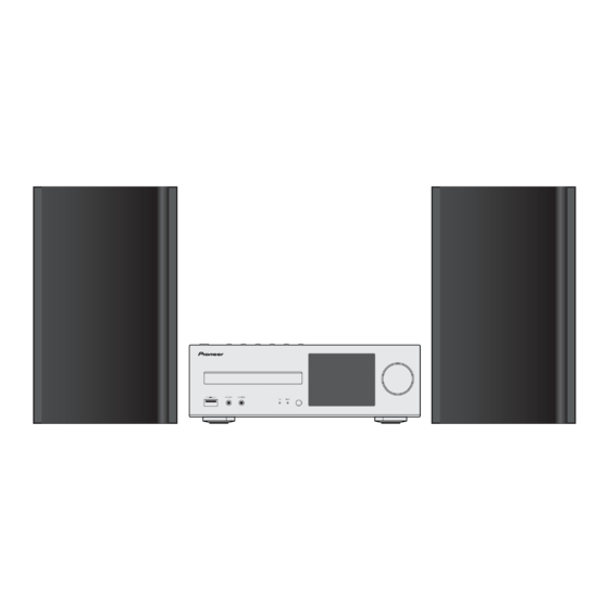
NETWORK CD RECEIVER SYSTEM
X-HM82-K
X-HM82-S
X-HM72-K,-S X-HM72D-K,-S
NETWORK CD RECEIVER
XC-HM82-K,-S
XC-HM82D-K
SPEAKER SECTION
S-HM82GB,S-HM82SA,S-HM72
THIS MANUAL IS APPLICABLE TO THE FOLLOWING MODEL(S) AND TYPE(S).
Model
Type
X-HM82-K, -S
SYXEV8
X-HM82-S
AXEV5
X-HM82D-K
VXEV8
XC-HM82-K, -S
SYXEV8
XC-HM82-K
CXEV
XC-HM82D-K
VXEV8
X-HM72-K, -S
SYXEV8
X-HM72D-K
VXEV8
X-HM72D-S
YXEV8
S-HM82GB
SYXEV8
S-HM82GB
VXEV8
S-HM82SA
AXEV5
S-HM72
SYXEV8
S-HM72
YXEV8
S-HM72
VXEV8
PIONEER CORPORATION
PIONEER ELECTRONICS (USA) INC. P.O. Box 1760, Long Beach, CA 90801-1760, U.S.A.
PIONEER EUROPE NV Haven 1087, Keetberglaan 1, 9120 Melsele, Belgium
PIONEER ELECTRONICS ASIACENTRE PTE. LTD. 253 Alexandra Road, #04-01, Singapore 159936
PIONEER CORPORATION 2014
Power Requirement
AC 220 V to 230 V
AC 220 V to 230 V
AC 220 V to 230 V
AC 220 V to 230 V
AC 120 V
AC 220 V to 230 V
AC 220 V to 230 V
AC 220 V to 230 V
AC 220 V to 230 V
1-1, Shin-ogura, Saiwai-ku, Kawasaki-shi, Kanagawa 212-0031, Japan
X-HM82-K
X-HM82D-K
Serial No.
&&&&######YY
&&&&######CN
&&&&######GB
&&&&######YY
&&&&######UC
&&&&######GB
&&&&######YY
&&&&######GB
&&&&######YY
ORDER NO.
RRV4574
Remarks
YY:Europe
CN:China
GB:U.K
YY:Europe
UC:North America
GB:U.K
YY:Europe
GB:U.K
YY:Europe
K-FZV OCT.
2014 Printed in Japan
Advertisement
Table of Contents

Related Manuals for Pioneer S-HM72


Summarization of Contents
SPEAKER SECTION
S-HM82GB, S-HM82SA, S-HM72
Details on speaker models covered by the manual.
SAFETY INFORMATION
WARNING
Important safety warnings regarding product content and handling.
1. SERVICE PRECAUTIONS
1.1 NOTES ON SOLDERING
Guidelines for safe and effective soldering with lead-free solder.
1. SERVICE PRECAUTIONS
1.2 NOTE ON REPLACING CD MECHA
Procedures for removing and installing the CD mecha unit safely.
1. SERVICE PRECAUTIONS
1.3 NOTES ON REPLACING CX870 MODULE
Information regarding MAC address changes after replacing the CX870 module.
1. SERVICE PRECAUTIONS
1.5 NOTE ON REPLACING DMAIN ASSY OR USB ASSY
Precautions for replacing DMAIN and USB assemblies, focusing on cable compatibility.
2. SPECIFICATIONS
2.1 ACCESSORIES
List of included accessories with part numbers.
2. SPECIFICATIONS
2.2 SPECIFICATIONS
Detailed technical specifications of the unit's various sections.
3. BASIC ITEMS FOR SERVICE
3.1 CHECK POINTS AFTER SERVICING
Essential checks to perform after completing service on the unit.
3. BASIC ITEMS FOR SERVICE
3.3 PCB LOCATIONS
Identification and location of main PCBs within the unit.
4. BLOCK DIAGRAM
4.1 OVERALL CONNECTION DIAGRAM
High-level overview of how different internal units are connected.
4. BLOCK DIAGRAM
4.2 BLOCK DIAGRAM
Detailed block diagram illustrating system components and data flow.
5. DIAGNOSIS
5.1 TROUBLESHOOTING
Step-by-step guide for diagnosing and resolving common operational issues.
5.2 PROTECTION CIRCUIT
5.2 PROTECTION CIRCUIT
Explanation of protection circuit functions and LED indicators.
5.3 POWER MANAGEMENT
Status Transition Diagram of Network Standby Mode and Bluetooth Standby Mode
Visual representation of power mode transitions.
5.4 CHECKING TERMINALS
1. Checking the LAN terminal
Procedure to verify the functionality of the unit's LAN terminal.
5.4 CHECKING TERMINALS
3. Checking the Built-in Bluetooth Module
Procedure to verify the Bluetooth module's connectivity and pairing.
5.5 IC INFORMATION
Pin Function
Detailed pin assignments and functions for the main microcontroller (IC5).
6. SERVICE MODE
6.1 SERVICE MODE
Instructions on entering and operating the unit's service mode.
6. SERVICE MODE
6.2 PROTECT CHECK MODE
Details on canceling operation lock and protection circuit indications.
6.3 CHECKING THE LCD
How to perform LCD checking
Procedure for testing the unit's LCD display using test modes.
7. DISASSEMBLY
Discharge
Steps for safely discharging the unit before diagnosis or repair.
7. DISASSEMBLY
[1] Exterior
Steps for removing exterior panels like the cabinet top and front section.
7. DISASSEMBLY
[2] CD ASSY, CD Mecha
Steps for removing the CD assembly and CD mecha.
7. DISASSEMBLY
[3] DMAIN ASSY, CNT1 ASSY, CNT2 ASSY and CX870 Module
Steps to remove DMAIN, CNT1, CNT2, and CX870 modules.
7. DISASSEMBLY
[6] MAIN ASSY
Steps for removing the MAIN assembly, including related components.
7. DISASSEMBLY
[7] FRONT ASSY, LCD Display
Steps for removing the front assembly and LCD display.
8. EACH SETTING AND ADJUSTMENT
8.1 UPDATING OF THE FIRMWARE
Steps for updating the MAIN microcomputer firmware.
8.1 UPDATING OF THE FIRMWARE
Updating of the Subcom, BCO firmware
Procedure for updating Subcom and BCO firmware using USB memory.
8.1 UPDATING OF THE FIRMWARE
Updating of the CD I/F, CD DSP Microcomputers firmware
Steps to update CD I/F and CD DSP microcomputer firmware via CD.
8.2 INITIAL SETTING
Setting Name
Table detailing various settings and their initial values.
8.3 IR BUTTON LIST
IR Button List of Network Hi Micro
Mapping of remote control buttons to functions for HM72/82 and past models.
9. EXPLODED VIEWS AND PARTS LIST
9.1 PACKING SECTION
Exploded view and parts list for the packing and main unit assembly.
10. SCHEMATIC DIAGRAM
10.1 MAIN ASSY (1/4)
Schematic diagram of the main assembly, part 1 of 4.
10.9 FRONT ASSY, KEY ASSY and USB ASSY
D FRONT ASSY
PCB connection diagram for the Front Assy.
10.9 FRONT ASSY, KEY ASSY and USB ASSY
E KEY ASSY
PCB connection diagram for the Key Assy.
F USB ASSY
PCB connection diagram for the USB Assy.
10.13 WAVEFORMS
A MAIN ASSY
Waveforms measured on the MAIN ASSY for troubleshooting.
10.13 WAVEFORMS
A MAIN ASSY
Waveforms measured on the MAIN ASSY for troubleshooting.
10.13 WAVEFORMS
B DMAIN ASSY
Waveforms measured on the DMAIN ASSY for troubleshooting.
10.13 WAVEFORMS
IC601 PIN. 5,8,6
Waveforms related to IC601, showing power on/off states.
11. PCB CONNECTION DIAGRAM
11.1 MAIN ASSY
PCB connection diagram for the main assembly (Side A).
11.1 MAIN ASSY
SIDE A
PCB connection diagram for the main assembly (Side A) and connector details.
11.1 MAIN ASSY
SIDE B
PCB connection diagram for the main assembly (Side B).
11.2 DMAIN ASSY and USB ASSY
SIDE A
PCB connection diagrams for DMAIN ASSY and USB ASSY (Side A).
11.2 DMAIN ASSY and USB ASSY
SIDE B
PCB connection diagrams for DMAIN ASSY and USB ASSY (Side B).
11.3 CD ASSY
SIDE A
PCB connection diagram for the CD ASSY (Side A).
11.4 FRONT ASSY and KEY ASSY
SIDE A
PCB connection diagrams for FRONT ASSY (Side A).
11.4 FRONT ASSY and KEY ASSY
SIDE A
PCB connection diagrams for KEY ASSY (Side A).
11.5 SMPS ASSY and CNT1 ASSY
SIDE A
PCB diagrams for SMPS ASSY and CNT1 ASSY (Side A).
11.5 SMPS ASSY and CNT1 ASSY
SIDE B
PCB diagrams for SMPS ASSY and CNT1 ASSY (Side B).
11.6 CNT2 ASSY
SIDE A
PCB connection diagrams for CNT2 ASSY (Side A).
11.7 USB GUIDE ASSY, GUIDE1 ASSY and GUIDE2 ASSY
SIDE A
PCB diagrams for USB GUIDE, GUIDE1, and GUIDE2 ASSY (Side A).
Need help?
Do you have a question about the S-HM72 and is the answer not in the manual?
Questions and answers