Table of Contents
Advertisement
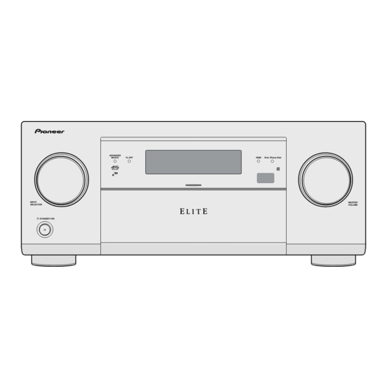
AV RECEIVER
SC-65
SC-1527-K
SC-1522-K
THIS MANUAL IS APPLICABLE TO THE FOLLOWING MODEL(S) AND TYPE(S).
Model
SC-65
UXJCB
SC-1527-K
CUXJ
SC-1522-K
UXJCB
PIONEER CORPORATION
PIONEER ELECTRONICS (USA) INC. P.O. Box 1760, Long Beach, CA 90801-1760, U.S.A.
PIONEER EUROPE NV Haven 1087, Keetberglaan 1, 9120 Melsele, Belgium
PIONEER ELECTRONICS ASIACENTRE PTE. LTD. 253 Alexandra Road, #04-01, Singapore 159936
PIONEER CORPORATION
INPUT
SELECTOR
STANDBY /ON
Type
Power Requirement
AC 120V
AC 120V
AC 120V
1-1, Shin-ogura, Saiwai-ku, Kawasaki-shi, Kanagawa 212-0031, Japan
2012
ADVANCED
MCACC
FL OFF
HDMI
iPod iPhone iPad
MASTER
VOLUME
SC-65
Remarks
ORDER NO.
RRV4311
K-FZV JUNE
2012 Printed in Japan
Advertisement
Table of Contents

Related Manuals for Pioneer SC-1527-K


Summarization of Contents
Safety Information
1. Service Precautions
Guidelines for handling and repairing the unit safely, including soldering and replacing parts.
Specifications
2.1 SC-65 Specifications
Detailed technical specifications for the SC-65 model, covering amplifier, audio, tuner, and video sections.
2.2 SC-1527-K/SC-1522-K Specifications
Detailed technical specifications for SC-1527-K and SC-1522-K models, covering amplifier, audio, tuner, and video sections.
Basic Items for Service
3.1 Check Points After Servicing
Recommended checks to perform after servicing the unit to ensure proper function and quality.
3.2 PCB Locations
Visual guide to the locations of various Printed Circuit Boards (PCBs) within the unit.
Diagnosis
5.1 Diagnosis Flowchart
Step-by-step troubleshooting guide for diagnosing common issues like "NO POWER".
5.2 Circuit Description
Detailed description of the protection circuit process lists for various amplifier stages.
Service Mode
6.1 Test Mode
Explains how to enter TEST MODE and displays the detected protection history.
Disassembly
7. Disassembly
General notes and procedures for disassembling the unit, including ground points.
[1] Front Section
Instructions for removing the front section, including bonnet and cables.
[2] Rear Section
Instructions for removing the rear panel.
[3] D-AMP_S ASSY
Procedures for removing the D-AMP_S Assy, including IR cover.
[4] DIGITAL MAIN ASSY
Procedures for removing the DIGITAL MAIN Assy, including cables and bonnet.
[5] DAC HIGH ASSY
Procedures for removing the DAC HIGH Assy, including bridge assemblies and screws.
Each Setting and Adjustment
8.1 Adjustment Required When the Unit is Repaired or Replaced
Details adjustments required after replacing components like DISPLAY ASSY, DIGITAL MAIN ASSY, or D-AMP_S ASSY.
How to Save and Load the Setting Using Backup Function with USB Memory
[How to save in the USB memory from AV amplifier]
Step-by-step procedure for saving unit settings to USB memory.
[How to write into AV amplifier from the USB memory]
Step-by-step procedure for loading saved settings from USB memory to the AV receiver.
Region Writing
8.3 Region Writing
Procedure to write region information using a USB memory, typically after replacing the DISPLAY Assy.
How to Update Firmware
UPDATE PANEL Mode (Version update)
Explains how to enter UPDATE PANEL mode for firmware updates and confirms the version.
Exploded Views and Parts List
9.1 Packing Section
Exploded view and parts list for the packing section of the unit.
9.2 Exterior Section
Exploded view showing the exterior parts of the unit and their assembly.
9.3 Rear Section
Exploded view illustrating the rear panel parts and their layout.
9.4 Chassis Section
Exploded view showing the internal chassis parts and their assembly.
9.5 Front Section
Exploded view illustrating the front panel parts and their assembly.
Schematic Diagram
10.1 Audio Assy (1/3)
Schematic diagram for the Audio Assembly, Part 1 of 3, serving as a guide page.
10.2 Audio Assy (2/3)
Schematic diagram for the Audio Assembly, Part 2 of 3.
10.3 Audio Assy (3/3)
Schematic diagram for the Audio Assembly, Part 3 of 3.
10.4 DAC High Assy (1/2)
Schematic diagram for the DAC High Assy, Part 1 of 2.
10.5 DAC High Assy (2/2)
Schematic diagram for the DAC High Assy, Part 2 of 2.
10.6 Front HDMI USB Assy
Schematic diagram for the Front HDMI USB Assy.
10.7 USB Rect Assy
Schematic diagram for the USB Rect Assy.
10.8 Digital Main Assy (1/11)
Schematic diagram for the Digital Main Assy, Part 1 of 11.
10.9 Digital Main Assy (2/11)
Schematic diagram for the Digital Main Assy, Part 2 of 11.
10.10 Digital Main Assy (3/11)
Schematic diagram for the Digital Main Assy, Part 3 of 11.
10.11 Digital Main Assy (4/11)
Schematic diagram for the Digital Main Assy, Part 4 of 11.
10.12 Digital Main Assy (5/11)
Schematic diagram for the Digital Main Assy, Part 5 of 11.
10.13 Digital Main Assy (6/11)
Schematic diagram for the Digital Main Assy, Part 6 of 11.
10.14 Digital Main Assy (7/11)
Schematic diagram for the Digital Main Assy, Part 7 of 11.
10.15 Digital Main Assy (8/11)
Schematic diagram for the Digital Main Assy, Part 8 of 11.
10.16 Digital Main Assy (9/11)
Schematic diagram for the Digital Main Assy, Part 9 of 11.
10.17 Digital Main Assy (10/11)
Schematic diagram for the Digital Main Assy, Part 10 of 11.
10.18 Digital Main Assy (11/11)
Schematic diagram for the Digital Main Assy, Part 11 of 11.
10.19 Interface Assy
Schematic diagram for the Interface Assy.
10.20 Component Assy (1/2)
Schematic diagram for the Component Assy, Part 1 of 2.
10.21 Component Assy (2/2)
Schematic diagram for the Component Assy, Part 2 of 2.
10.22 Composite Assy
Schematic diagram for the Composite Assy.
10.23 Mic HP Assy
Schematic diagram for the Mic HP Assy.
10.24 Display Assy (1/2)
Schematic diagram for the Display Assy, Part 1 of 2.
10.25 Display Assy (2/2)
Schematic diagram for the Display Assy, Part 2 of 2.
10.26 Vol Assy and Power SW Assy
Schematics for the Volume and Power Switch assemblies.
10.27 Encoder Assy
Schematic diagram for the Encoder Assy.
10.28 IR Buffer Assy (1/2)
Schematic diagram for the IR Buffer Assy, Part 1 of 2.
10.29 IR Buffer Assy (2/2)
Schematic diagram for the IR Buffer Assy, Part 2 of 2.
10.30 Buffer GND Assy and IR Interface Assy
Schematics for the Buffer GND and IR Interface assemblies.
10.31 D-AMP_S Assy (1/10)
Schematic diagram for the D-AMP_S Assy, Part 1 of 10.
10.31 D-AMP_S Assy (2/10)
Schematic diagram for the D-AMP_S Assy, Part 2 of 10.
10.31 D-AMP_S Assy (3/10)
Schematic diagram for the D-AMP_S Assy, Part 3 of 10.
10.31 D-AMP_S Assy (4/10)
Schematic diagram for the D-AMP_S Assy, Part 4 of 10.
10.31 D-AMP_S Assy (5/10)
Schematic diagram for the D-AMP_S Assy, Part 5 of 10.
10.31 D-AMP_S Assy (6/10)
Schematic diagram for the D-AMP_S Assy, Part 6 of 10.
10.31 D-AMP_S Assy (7/10)
Schematic diagram for the D-AMP_S Assy, Part 7 of 10.
10.31 D-AMP_S Assy (8/10)
Schematic diagram for the D-AMP_S Assy, Part 8 of 10.
10.31 D-AMP_S Assy (9/10)
Schematic diagram for the D-AMP_S Assy, Part 9 of 10.
10.31 D-AMP_S Assy (10/10)
Schematic diagram for the D-AMP_S Assy, Part 10 of 10.
11. PCB Connection Diagram
PCB connection diagrams for various assemblies like Audio, Digital Main, and DAC High.
11.1 Audio Assy
PCB connection diagram for the Audio Assy, showing connector pin assignments.
11.2 DAC High Assy (1/2)
PCB connection diagram for the DAC High Assy, Part 1 of 2.
11.2 DAC High Assy (2/2)
PCB connection diagram for the DAC High Assy, Part 2 of 2.
11.3 Front HDMI USB Assy
PCB connection diagram for the Front HDMI USB Assy.
11.4 USB Rect Assy
PCB connection diagram for the USB Rect Assy.
11.5 Digital Main Assy (1/11)
PCB layout diagram for the Digital Main Assy, Part 1 of 11.
11.5 Digital Main Assy (2/11)
PCB layout diagram for the Digital Main Assy, Part 2 of 11.
11.6 Interface Assy
PCB layout diagram for the Interface Assy.
11.7 Component Assy (1/2)
PCB layout diagram for the Component Assy, Part 1 of 2.
11.7 Component Assy (2/2)
PCB layout diagram for the Component Assy, Part 2 of 2.
11.8 Composite Assy
PCB layout diagram for the Composite Assy.
11.9 Mic HP Assy
PCB layout diagram for the MIC HP Assy.
11.10 Digital Main Assy (3/11)
PCB layout diagram for the Digital Main Assy, Part 3 of 11.
11.10 Digital Main Assy (4/11)
PCB layout diagram for the Digital Main Assy, Part 4 of 11.
11.10 Digital Main Assy (5/11)
PCB layout diagram for the Digital Main Assy, Part 5 of 11.
11.10 Digital Main Assy (6/11)
PCB layout diagram for the Digital Main Assy, Part 6 of 11.
11.10 Digital Main Assy (7/11)
PCB layout diagram for the Digital Main Assy, Part 7 of 11.
11.10 Digital Main Assy (8/11)
PCB layout diagram for the Digital Main Assy, Part 8 of 11.
11.10 Digital Main Assy (9/11)
PCB layout diagram for the Digital Main Assy, Part 9 of 11.
11.10 Digital Main Assy (10/11)
PCB layout diagram for the Digital Main Assy, Part 10 of 11.
11.10 Digital Main Assy (11/11)
PCB layout diagram for the Digital Main Assy, Part 11 of 11.
11.11 Vol, Power SW and Encoder Assys
PCB layouts for Volume, Power Switch, and Encoder assemblies.
11.12 IR Buffer Assy (1/2)
PCB layout diagram for the IR Buffer Assy, Part 1 of 2.
11.12 IR Buffer Assy (2/2)
PCB layout diagram for the IR Buffer Assy, Part 2 of 2.
11.13 Buffer GND Assy and IR Interface Assy
PCB layouts for Buffer GND and IR Interface assemblies.
11.14 D-AMP_S Assy (1/10)
PCB layout diagram for the D-AMP_S Assy, Part 1 of 10.
11.14 D-AMP_S Assy (2/10)
PCB layout diagram for the D-AMP_S Assy, Part 2 of 10.
11.15 Primary Assy
PCB layout diagram for the Primary Assy.
11.15 Primary Assy
Continuation of the Primary Assy PCB layout.
11.16 A-Reg Assy
PCB layout diagram for the A-REG Assy.
11.17 IR Reg Assy (1/2)
PCB layout diagram for the IR REG Assy, Part 1 of 2.
11.17 IR Reg Assy (2/2)
PCB layout diagram for the IR REG Assy, Part 2 of 2.
11.18 V-Reg Assy (3/3)
PCB layout diagram for the V-REG Assy, Part 3 of 3.
11.19 Vreg Child Assy and Connect Assy
PCB layouts for VREG Child and Connect assemblies.
11.20 A-DAC Bridge, D-Audio Bridge, D-DAC Bridge and Pre Bridge Assys
PCB layouts for A-DAC, D-AUDIO, D-DAC, and PRE BRIDGE assemblies.
Need help?
Do you have a question about the SC-1527-K and is the answer not in the manual?
Questions and answers