Table of Contents
Advertisement
SERVICE MANUAL
Ver. 1.4 2006. 05
• The tuner and CD sections have no adjustments.
AUDIO POWER SPECIFICATIONS (US, Canadian model)
POWER OUTPUT AND TOTAL HARMONIC DISTORTION
23.2 watts per channel minimum continuous average power into
4 ohms, 4 channels driven from 20 Hz to 20 kHz with no more
than 5% total harmonic distortion.
CD Player section
Signal-to-noise ratio:
120 dB
Frequency response:
10 – 20,000 Hz
Wow and flutter:
Below measurable limit
Tuner section
FM
Tuning range
CDX-GT10W/GT100 (US, Canadian):
87.5 – 107.9 MHz
CDX-GT100 (AEP, UK):
87.5 – 108.0 MHz
CDX-GT150/GT150S:
87.5 – 108.0 MHz (at 50 kHz step)
87.5 – 107.9 MHz (at 200 kHz step)
FM tuning interval
CDX-GT150/GT150S:
50 kHz/200 kHz switchable
Antenna terminal:
External antenna connector
Intermediate frequency: 10.7 MHz/450 kHz
Usable sensitivity:
9 dBf
Selectivity:
75 dB at 400 kHz
Signal-to-noise ratio:
67 dB (stereo), 69 dB (mono)
Harmonic distortion at 1 kHz:
0.5 % (stereo), 0.3 % (mono)
Separation:
35 dB at 1 kHz
Frequency response:
30 – 15,000 Hz
Sony Corporation
9-879-863-05
2006E04-1
eVehicle Division
© 2006. 05
Published by Sony Techno Create Corporation
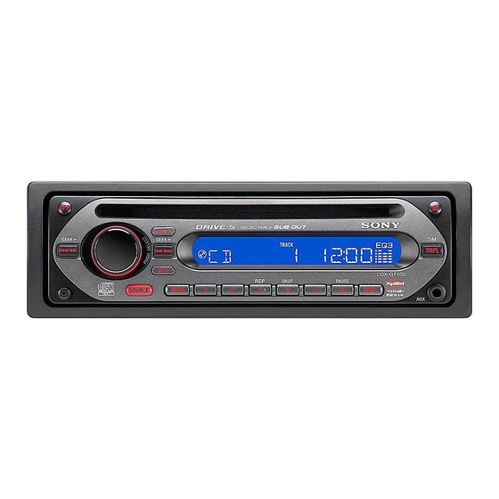
CDX-GT10W/GT100/
(Photo: CDX-GT100)
Model Name Using Similar Mechanism
CD Drive Mechanism Type
Optical Pick-up Name
SPECIFICATIONS
AM (CDX-GT10W/GT100 (US, Canadian)/GT150/GT150S)
Tuning range
Antenna terminal:
Intermediate frequency: 10.7 MHz/450 kHz
Sensitivity:
MW/LW (CDX-GT100 (AEP, UK))
Tuning range:
Aerial terminal:
Intermediate frequency: 10.7 MHz/450 kHz
Sensitivity:
Power amplifier section
Outputs:
Speaker impedance:
Maximum power output: 52 W × 4 (at 4 ohms)
FM/AM COMPACT DISC PLAYER
CDX-GT10W/GT100: US,CND/GT150/GT150S
FM/MW/LW COMPACT DISC PLAYER
GT150/GT150S
US Model
Canadian Model
CDX-GT10W/GT100
AEP Model
UK Model
E Model
Chinese Model
CDX-GT150/GT150S
NEW
MG-611XE-186//C
MG-611XE-186//Q
KSS1000E
CDX-GT10W/GT100 (US, Canadian):
530 – 1,710 kHz
CDX-GT150/GT150S:
531 – 1,602 kHz (at 9 kHz step)
530 – 1,710 kHz (at 10 kHz step)
External antenna connector
30 µV
MW: 531 – 1,602 kHz
LW: 153 – 279 kHz
External aerial connector
MW: 30 µV, LW: 40 µV
Speaker outputs (sure seal connectors)
4 – 8 ohms
(CDX-GT10W/GT100 (US, Canadian)/GT150)
45 W × 4 (at 4 ohms) (CDX-GT100 (AEP, UK)/GT150S)
– Continued on next page –
CDX-GT100: AEP,UK
CDX-GT100
1
Advertisement
Chapters
Table of Contents

Related Manuals for Sony CDX-GT150S


Summarization of Contents
Specifications
CD Player Section Specifications
Technical specifications for the CD playback component.
Tuner Section Specifications
Technical specifications for FM and AM/MW/LW tuning.
Power Amplifier Section Specifications
Technical specifications for the audio output power.
Service Notes and Precautions
Optical Pick-up Handling Precautions
Precautions for handling the optical pick-up block.
Laser Diode Emission Check
Guidelines for safely checking laser diode emission.
Chip Component Replacement Advice
Advice for replacing surface-mount chip components.
Safety Component Warning
Warning about safety-critical components.
Solder and Service Procedures
Unleaded Solder Information
Information and characteristics of unleaded solder.
Extension Cable for Service
Instructions for connecting extension cable for servicing.
Section 1 General
Controls Location (CDX-GT10W/GT100)
Identifies controls and basic operations for the main unit.
Controls Location (CDX-GT150/GT150S)
Identifies controls and basic operations for the main unit.
Connections
Connection Diagram and Notes
Visual guide and notes for unit connectivity.
Section 2 Disassembly
Disassembly Sequence
Step-by-step procedure for disassembling the set.
2-1. Sub Panel Assy Disassembly
Procedure for disassembling the sub panel assembly.
2-2. CD Mechanism Block Disassembly
Procedure for disassembling the CD mechanism block.
2-3. Main Board Disassembly
Procedure for disassembling the main board.
2-4. Chassis (T) Sub Assy Disassembly
Procedure for disassembling the chassis (T) sub assembly.
2-5. Roller Arm Assy Disassembly
Procedure for disassembling the roller arm assembly.
2-6. Chassis (OP) Assy Disassembly
Procedure for disassembling the chassis (OP) assembly.
2-7. Optical Pick-up Disassembly
Procedure for disassembling the optical pick-up.
2-8. SL Motor Assy (M902) Disassembly
Procedure for disassembling the SL motor assembly.
2-9. LE Motor Assy (M903) Disassembly
Procedure for disassembling the LE motor assembly.
2-10. Servo Board Disassembly
Procedure for disassembling the servo board.
Section 3 Diagrams
3-1. Block Diagram - CD Section
Block diagram illustrating the CD section circuitry.
3-2. Block Diagram - Main Section
Block diagram illustrating the main section circuitry.
3-3. Block Diagram - Display Section
Block diagram illustrating the display section circuitry.
3-4. Circuit Boards Location
Diagrams showing the location of all circuit boards.
3-5. Printed Wiring Boards - CD Mechanism Section
Printed wiring board layout for the CD mechanism section.
3-6. Schematic Diagram - CD Mechanism Section
Schematic diagram for the CD mechanism section.
3-7. Printed Wiring Board - Main Section
Printed wiring board layout for the main section.
3-8. Schematic Diagram - Main Section (1/3)
Schematic diagram for the main section, part 1 of 3.
3-9. Schematic Diagram - Main Section (2/3)
Schematic diagram for the main section, part 2 of 3.
3-10. Schematic Diagram - Main Section (3/3)
Schematic diagram for the main section, part 3 of 3.
3-11. Printed Wiring Boards - Key Section
Printed wiring board layout for the key section.
3-12. Schematic Diagram - Key Section
Schematic diagram for the key section.
Waveforms and IC Block Diagrams
Servo Board Waveforms
Waveforms from the servo board for CD playback.
Main Board Waveforms
Waveforms from the main board.
IC Block Diagrams
Block diagrams for key integrated circuits.
IC Pin Descriptions
IC1 µPD63712GC-8EU-A (SERVO BOARD)
Pin descriptions for IC1 on the servo board.
Section 4 Exploded Views
4-1. Main Section Exploded View
Exploded view of the main section of the unit.
4-2. Front Panel Section Exploded View
Exploded view of the front panel assembly.
4-3. CD Mechanism Section (1) Exploded View
Exploded view of CD mechanism section 1.
4-4. CD Mechanism Section (2) Exploded View
Exploded view of CD mechanism section 2.
4-5. CD Mechanism Section (3) Exploded View
Exploded view of CD mechanism section 3.
4-6. CD Mechanism Section (4) Exploded View
Exploded view of CD mechanism section 4.
Section 5 Electrical Parts List
Electrical Parts - Jack Board
List of electrical parts for the jack board.
Electrical Parts - Key Board
List of electrical parts for the key board.
Electrical Parts - Diode
List of diodes used in the unit.
Electrical Parts - Switch
List of switches used in the unit.
Supplement-1
Model Discrimination
Information to discriminate between different production models.
Section 1 Diagrams
Waveforms and IC Block Diagrams
Waveforms and block diagrams for key circuit sections.
Need help?
Do you have a question about the CDX-GT150S and is the answer not in the manual?
Questions and answers