Table of Contents
Advertisement
RX-V557/HTR-5850/DSP-AX557
RX-V457/HTR-5840/DSP-AX457
This manual has been provided for the use of authorized YAMAHA Retailers and their service personnel.
It has been assumed that basic service procedures inherent to the industry, and more specifically YAMAHA Products, are already
known and understood by the users, and have therefore not been restated.
WARNING:
IMPORTANT:
The data provided is believed to be accurate and applicable to the unit(s) indicated on the cover. The research, engineering, and
service departments of YAMAHA are continually striving to improve YAMAHA products. Modifications are, therefore, inevitable
and specifications are subject to change without notice or obligation to retrofit. Should any discrepancy appear to exist, please
contact the distributor's Service Division.
WARNING:
IMPORTANT:
I CONTENTS
TO SERVICE PERSONNEL .......................................... 2
FRONT PANELS ........................................................ 3~6
REAR PANELS ........................................................ 6~15
SPECIFICATIONS / 参考仕様 ................................ 16~18
INTERNAL VIEW ................................................... 18~19
REMOTE CONTROL PANELS .................................... 19
DISASSEMBLY PROCEDURES / 分解手順 ......... 20~23
自己診断機能(ダイアグ) ..................................... 24~44
1 0 0 9 4 1
AV RECEIVER/AV AMPLIFIER
IMPORTANT NOTICE
Failure to follow appropriate service and safety procedures when servicing this product may result in personal
injury, destruction of expensive components, and failure of the product to perform as specified. For these reasons,
we advise all YAMAHA product owners that any service required should be performed by an authorized
YAMAHA Retailer or the appointed service representative.
The presentation or sale of this manual to any individual or firm does not constitute authorization, certification or
recognition of any applicable technical capabilities, or establish a principle-agent relationship of any form.
Static discharges can destroy expensive components. Discharge any static electricity your body may have
accumulated by grounding yourself to the ground buss in the unit (heavy gauge black wires connect to this buss).
Turn the unit OFF during disassembly and part replacement. Recheck all work before you apply power to the unit.
SERVICE MANUAL
AMP ADJUSTMENT / アンプ部調整 ........................... 45
IC DATA ................................................................. 46~51
BLOCK DIAGRAM ................................................. 52~55
DISPLAY DATA ........................................................... 56
PRINTED CIRCUIT BOARD .................................. 57~79
PIN CONNECTION DIAGRAM .................................... 80
SCHEMATIC DIAGRAM ........................................ 81~93
PARTS LIST ......................................................... 95~129
REMOTE CONTROL .......................................... 130~131
P.O.Box 1, Hamamatsu, Japan
'05.03
Advertisement
Table of Contents

Related Manuals for Yamaha HTR5850 - XM-Ready A/V Surround Receiver


Summarization of Contents
TO SERVICE PERSONNEL
Critical Components Information
Information about components marked with s requiring specific replacement parts.
Leakage Current Measurement
Procedure for verifying insulation of exposed conductive surfaces on 120V models.
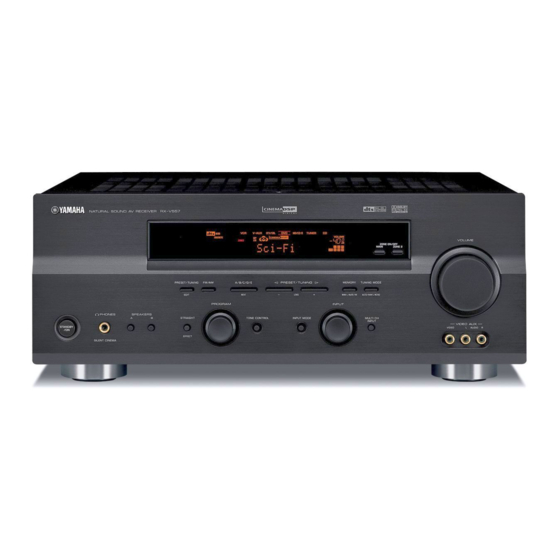
FRONT PANELS
RX-V557 (U, C models)
Illustration of the front panel for RX-V557 U and C model variants.
RX-V557 (R, T, K, A, B, G, E, L models)
Illustration of the front panel for RX-V557 R, T, K, A, B, G, E, L model variants.
REAR PANELS
RX-V557 (U, C models)
Illustration of the rear panel for RX-V557 U and C model variants.
SPECIFICATIONS / 参考仕様
Audio Section / オーディオ部
Detailed specifications for the audio amplifier section, including output power and frequency response.
Video Section / ビデオ部
Specifications related to video signal types, levels, and conversion.
INTERNAL VIEW
■ Set Menu Table / セットメニュー
A table detailing the setup menu items, sub-menus, select menus, and initial values.
■ INPUT MENU
Lists input assignments for various terminals and input modes.
■ OPTION MENU
Covers display settings, memory guard, parameter initialization, and multi-zone settings.
REMOTE CONTROL PANELS
RX-V557 (U, C, R, T, K, A, L models), HTR-5850 (U, C, T, K, A models), DSP-AX557 (J model)
Diagrams of remote control panels for specific RX-V557, HTR-5850, and DSP-AX557 models.
RX-V457 (U, C, R, T, K, A, L models), HTR-5840 (U, C, T, K, A models), DSP-AX457 (J model)
Diagrams of remote control panels for specific RX-V457, HTR-5840, and DSP-AX457 models.
RX-V457 (B, G, E models), HTR-5840 (B, G, E models), RX-V557 (B, G, E models)
Diagrams of remote control panels for specific RX-V457, HTR-5840, and RX-V557 models (B, G, E variants).
DISASSEMBLY PROCEDURES / 分解手順
1. Removal of Top Cover
Instructions for removing the top cover of the unit.
2. Removal of Front Panel Unit
Instructions for removing the front panel unit.
3. Removal of Plate Side
Instructions for removing the side plates.
SELF DIAGNOSIS FUNCTION (DIAG) / 自己診断機能(ダイアグ)
1 BYPASS
BYPASS menu items: ANALOG BYPASS, DSP BYPASS.
2 RAM THROUGH
RAM THROUGH menu items: RAM MARGIN, RAM FULL BIT.
3 PRO LOGIC
PRO LOGIC menu items: PRO LOGIC.
4 SPEAKERS SET
SPEAKERS SET controls analog switch settings for different speaker configurations.
10. AD DATA CHECK
DC/PS (protection detection)
DC/PS section details DC and power supply voltage protection values.
THM (temperature detection)
THM section details temperature detection values and normal voltage references.
Operation procedure of DIAG menu and SUB-MENU
DIAG menu selection
Method for selecting the main DIAG menu item using the PROGRAM knob.
SUB-MENU selection
Method for selecting sub-menu items using PRESET/TUNING keys.
Initial settings used to start DIAG
Initial settings applied when starting the DIAG mode.
Details of DIAG menu
1. BYPASS
BYPASS menu allows selection between analog bypass and DSP bypass output.
18. SOFT SW
SW MODE
SW MODE allows selection between PCB, MODEL, or FNC settings.
MODEL SETTING
MODEL SETTING selects between different model types for the unit.
DESTINATION
DESTINATION selects the market region for the unit.
AMP ADJUSTMENT / アンプ部調整
Confirmation of Idling Current of MAIN (1) P. C. B.
Procedure to confirm and adjust the idling current of the MAIN (1) P.C.B.
IC DATA
IC5 : D60YA003BPYP225 (DSP P.C.B.) Decoder
Pin multiplexing and digital signal processor block diagram for IC5 (DSP).
BLOCK DIAGRAM (2/2)
OPERATION (2)
Block diagram section for the Operation (2) unit.
SUBTRANS (3)
Block diagram section for Subtrans (3) unit.
SUBTRANS (6)
Block diagram section for Subtrans (6) unit.
BLOCK DIAGRAM (2/2)
OPERATION (2)
Block diagram section for Operation (2) unit (RX-V457/HTR-5840/DSP-AX457).
SUBTRANS (3)
Block diagram section for Subtrans (3) unit (RX-V457/HTR-5840/DSP-AX457).
SUBTRANS (6)
Block diagram section for Subtrans (6) unit (RX-V457/HTR-5840/DSP-AX457).
DISPLAY DATA
■ PIN CONNECTION
Table detailing pin connections.
PRINTED CIRCUIT BOARD (Foil side)
DSP P.C.B. (Side A)
Printed circuit board layout for DSP P.C.B. (Side A).
DSP P.C.B. (Side B)
Printed circuit board layout for DSP P.C.B. (Side B).
■ Semiconductor Location
List of semiconductor locations on the DSP P.C.B.
PRINTED CIRCUIT BOARD (Foil side)
FUNCTION P.C.B. (Side A)
Printed circuit board layout for FUNCTION P.C.B. (Side A).
FUNCTION P.C.B. (Side B)
Printed circuit board layout for FUNCTION P.C.B. (Side B).
PRINTED CIRCUIT BOARD (Foil side)
FUNCTION P.C.B. (Side B)
Printed circuit board layout for FUNCTION P.C.B. (Side B).
PRINTED CIRCUIT BOARD (Foil side)
OPERATION (1) P.C.B. (Side A)
Printed circuit board layout for OPERATION (1) P.C.B. (Side A).
OPERATION (1) P.C.B. (Side B)
Printed circuit board layout for OPERATION (1) P.C.B. (Side B).
PRINTED CIRCUIT BOARD (Foil side)
OPERATION (2) P.C.B. (Side A)
Printed circuit board layout for OPERATION (2) P.C.B. (Side A).
OPERATION (3) P.C.B. (Side A)
Printed circuit board layout for OPERATION (3) P.C.B. (Side A).
OPERATION (3) P.C.B. (Side B)
Printed circuit board layout for OPERATION (3) P.C.B. (Side B).
PRINTED CIRCUIT BOARD (Foil side)
OPERATION (1) P.C.B. (Side A)
Printed circuit board layout for OPERATION (1) P.C.B. (Side A) for HTR-5850/RX-V457 models.
OPERATION (1) P.C.B. (Side B)
Printed circuit board layout for OPERATION (1) P.C.B. (Side B) for HTR-5850/RX-V457 models.
PRINTED CIRCUIT BOARD (Foil side)
OPERATION (2) P.C.B. (Side A)
Printed circuit board layout for OPERATION (2) P.C.B. (Side A).
OPERATION (3) P.C.B. (Side A)
Printed circuit board layout for OPERATION (3) P.C.B. (Side A).
OPERATION (3) P.C.B. (Side B)
Printed circuit board layout for OPERATION (3) P.C.B. (Side B).
PRINTED CIRCUIT BOARD (Foil side)
MAIN (1) P.C.B. (Side A)
Printed circuit board layout for MAIN (1) P.C.B. (Side A).
PRINTED CIRCUIT BOARD (Foil side)
MAIN (2) P.C.B. (Side A)
Printed circuit board layout for MAIN (2) P.C.B. (Side A).
PRINTED CIRCUIT BOARD (Foil side)
POWER (1) P.C.B. (Side A)
Printed circuit board layout for POWER (1) P.C.B. (Side A).
POWER (2) P.C.B. (Side A)
Printed circuit board layout for POWER (2) P.C.B. (Side A).
PRINTED CIRCUIT BOARD (Foil side)
SUBTRANS (1) P.C.B. (Side A)
Printed circuit board layout for SUBTRANS (1) P.C.B. (Side A).
SUBTRANS (1) P.C.B. (Side B)
Printed circuit board layout for SUBTRANS (1) P.C.B. (Side B).
SUBTRANS (3) P.C.B. (Side A)
Printed circuit board layout for SUBTRANS (3) P.C.B. (Side A).
SUBTRANS (3) P.C.B. (Side B)
Printed circuit board layout for SUBTRANS (3) P.C.B. (Side B).
PRINTED CIRCUIT BOARD (Foil side)
SUBTRANS (2) P.C.B. (Side A)
Printed circuit board layout for SUBTRANS (2) P.C.B. (Side A).
SUBTRANS (2) P.C.B. (Side B)
Printed circuit board layout for SUBTRANS (2) P.C.B. (Side B).
PRINTED CIRCUIT BOARD (Foil side)
SUBTRANS (6) P.C.B. (Side A)
Printed circuit board layout for SUBTRANS (6) P.C.B. (Side A).
SUBTRANS (6) P.C.B. (Side B)
Printed circuit board layout for SUBTRANS (6) P.C.B. (Side B).
SUBTRANS (7) P.C.B. (Side A)
Printed circuit board layout for SUBTRANS (7) P.C.B. (Side A).
SUBTRANS (7) P.C.B. (Side B)
Printed circuit board layout for SUBTRANS (7) P.C.B. (Side B).
PRINTED CIRCUIT BOARD (Foil side)
SUBTRANS (7) P.C.B. (Side A)
Printed circuit board layout for SUBTRANS (7) P.C.B. (Side A).
SUBTRANS (7) P.C.B. (Side B)
Printed circuit board layout for SUBTRANS (7) P.C.B. (Side B).
SUBTRANS (9) P.C.B. (Side A)
Printed circuit board layout for SUBTRANS (9) P.C.B. (Side A).
SUBTRANS (10) P.C.B. (Side A)
Printed circuit board layout for SUBTRANS (10) P.C.B. (Side A).
PRINTED CIRCUIT BOARD (Foil side)
SUBTRANS (1) P.C.B. (Side A)
Printed circuit board layout for SUBTRANS (1) P.C.B. (Side A) for HTR-5850.
SUBTRANS (1) P.C.B. (Side B)
Printed circuit board layout for SUBTRANS (1) P.C.B. (Side B) for HTR-5850.
SUBTRANS (3) P.C.B. (Side A)
Printed circuit board layout for SUBTRANS (3) P.C.B. (Side A) for HTR-5850.
SUBTRANS (3) P.C.B. (Side B)
Printed circuit board layout for SUBTRANS (3) P.C.B. (Side B) for HTR-5850.
PRINTED CIRCUIT BOARD (Foil side)
SUBTRANS (2) P.C.B. (Side A)
Printed circuit board layout for SUBTRANS (2) P.C.B. (Side A).
SUBTRANS (2) P.C.B. (Side B)
Printed circuit board layout for SUBTRANS (2) P.C.B. (Side B).
PRINTED CIRCUIT BOARD (Foil side)
SUBTRANS (6) P.C.B. (Side A)
Printed circuit board layout for SUBTRANS (6) P.C.B. (Side A).
SUBTRANS (7) P.C.B. (Side A)
Printed circuit board layout for SUBTRANS (7) P.C.B. (Side A).
SUBTRANS (9) P.C.B. (Side A)
Printed circuit board layout for SUBTRANS (9) P.C.B. (Side A).
SUBTRANS (10) P.C.B. (Side A)
Printed circuit board layout for SUBTRANS (10) P.C.B. (Side A).
PRINTED CIRCUIT BOARD (Foil side)
SUBTRANS (1) P.C.B. (Side A)
Printed circuit board layout for SUBTRANS (1) P.C.B. (Side A) for RX-V457/HTR-5840/DSP-AX457.
SUBTRANS (1) P.C.B. (Side B)
Printed circuit board layout for SUBTRANS (1) P.C.B. (Side B) for RX-V457/HTR-5840/DSP-AX457.
SUBTRANS (3) P.C.B. (Side A)
Printed circuit board layout for SUBTRANS (3) P.C.B. (Side A) for RX-V457/HTR-5840/DSP-AX457.
SUBTRANS (3) P.C.B. (Side B)
Printed circuit board layout for SUBTRANS (3) P.C.B. (Side B) for RX-V457/HTR-5840/DSP-AX457.
PRINTED CIRCUIT BOARD (Foil side)
SUBTRANS (2) P.C.B. (Side A)
Printed circuit board layout for SUBTRANS (2) P.C.B. (Side A).
SUBTRANS (2) P.C.B. (Side B)
Printed circuit board layout for SUBTRANS (2) P.C.B. (Side B).
PRINTED CIRCUIT BOARD (Foil side)
SUBTRANS (4) P.C.B. (Side A)
Printed circuit board layout for SUBTRANS (4) P.C.B. (Side A).
SUBTRANS (4) P.C.B. (Side B)
Printed circuit board layout for SUBTRANS (4) P.C.B. (Side B).
SUBTRANS (5) P.C.B. (Side A)
Printed circuit board layout for SUBTRANS (5) P.C.B. (Side A).
PRINTED CIRCUIT BOARD (Foil side)
SUBTRANS (6) P.C.B. (Side A)
Printed circuit board layout for SUBTRANS (6) P.C.B. (Side A).
SUBTRANS (6) P.C.B. (Side B)
Printed circuit board layout for SUBTRANS (6) P.C.B. (Side B).
SUBTRANS (7) P.C.B. (Side A)
Printed circuit board layout for SUBTRANS (7) P.C.B. (Side A).
SUBTRANS (7) P.C.B. (Side B)
Printed circuit board layout for SUBTRANS (7) P.C.B. (Side B).
PRINTED CIRCUIT BOARD (Foil side)
CONVERSION P.C.B. (Side A)
Printed circuit board layout for CONVERSION P.C.B. (Side A).
CONVERSION P.C.B. (Side B)
Printed circuit board layout for CONVERSION P.C.B. (Side B).
PRINTED CIRCUIT BOARD (Foil side)
VIDEO P.C.B. (Side A)
Printed circuit board layout for VIDEO P.C.B. (Side A) for DSP-AX457.
VIDEO P.C.B. (Side A)
Printed circuit board layout for VIDEO P.C.B. (Side A) for DSP-AX457.
XM P.C.B. (Side A)
Printed circuit board layout for XM P.C.B. (Side A) for RX-V557/HTR-5850.
XM P.C.B. (Side B)
Printed circuit board layout for XM P.C.B. (Side B) for RX-V557/HTR-5850.
PIN CONNECTION DIAGRAM
• ICs
Diagrams showing pin connections for various integrated circuits (ICs).
• Diodes
Diagrams showing pin connections for various diodes.
• Transistors
Diagrams showing pin connections for various transistors.
SCHEMATIC DIAGRAM (DSP 1/2)
IC1: SN74LVU04APWR Hex Inverters
Schematic for IC1, SN74LVU04APWR Hex Inverters.
IC3: SN74AHCT00PWR Quad 2-Input Nand Gate
Schematic for IC3, SN74AHCT00PWR Quad 2-Input Nand Gate.
IC6: W9816G6CH 512K x 2 Banks x 16 Bits SDRAM
Schematic for IC6, W9816G6CH SDRAM.
SCHEMATIC DIAGRAM (DSP 2/2)
IC16: AK4628VQ 192kHz 24Bit 8-channel CODEC
Schematic for IC16, AK4628VQ 8-channel CODEC.
IC18, 21: NJM2068MD Dual OP-Amp
Schematic for IC18, 21, NJM2068MD Dual OP-Amp.
IC19, 20: NE5532DR DUAL LOW-NOISE OPERATIONAL AMPLIFIERS
Schematic for IC19, 20, NE5532DR Dual Low-Noise Op-Amps.
SCHEMATIC DIAGRAM (FUNCTION)
IC301: BD3816K1 7-channel volume IC for 7-channel
Schematic for IC301, BD3816K1 7-channel volume IC.
IC302: BD3841FS Function Switch
Schematic for IC302, BD3841FS Function Switch.
IC303, 304, 306: NJM2068MD Dual OP-Amp
Schematic for IC303, 304, 306, NJM2068MD Dual OP-Amp.
SCHEMATIC DIAGRAM (OPERATION)
IC801: M66003-0101FP FL Display Driver
Schematic for IC801, M66003-0101FP FL Display Driver.
SCHEMATIC DIAGRAM (OPERATION)
IC801: M66003-0101FP FL Display Driver
Schematic for IC801, M66003-0101FP FL Display Driver (HTR-5850/RX-V457 models).
SCHEMATIC DIAGRAM (POWER)
IC301: LM61CIZ Temperature Sensor
Schematic for IC301, LM61CIZ Temperature Sensor.
IC302: NJM7812FA Voltage Regulator
Schematic for IC302, NJM7812FA Voltage Regulator.
IC304: NJM7805FA Voltage Regulator
Schematic for IC304, NJM7805FA Voltage Regulator.
SCHEMATIC DIAGRAM (SUBTRANS)
IC401, 403: TLP421 Photo Transistor
Schematic for IC401, 403, TLP421 Photo Transistor.
IC402: TC4013BP Dual D-type Flip Flop
Schematic for IC402, TC4013BP Dual D-type Flip Flop.
IC452: NJU7201L55 Voltage Regulator
Schematic for IC452, NJU7201L55 Voltage Regulator.
SCHEMATIC DIAGRAM (SUBTRANS)
IC401, 403: TLP421 Photo Transistor
Schematic for IC401, 403, TLP421 Photo Transistor (HTR-5850).
IC402: TC4013BP Dual D-type Flip Flop
Schematic for IC402, TC4013BP Dual D-type Flip Flop (HTR-5850).
IC452: NJU7201L55 Voltage Regulator
Schematic for IC452, NJU7201L55 Voltage Regulator (HTR-5850).
SCHEMATIC DIAGRAM (SUBTRANS)
IC402: TC4013BP Dual D-type Flip Flop
Schematic for IC402, TC4013BP Dual D-type Flip Flop (RX-V457/HTR-5840/DSP-AX457).
IC452: NJU7201L55 Voltage Regulator
Schematic for IC452, NJU7201L55 Voltage Regulator (RX-V457/HTR-5840/DSP-AX457).
IC453: LC72722PM RDS Signal Processor
Schematic for IC453, LC72722PM RDS Signal Processor.
SCHEMATIC DIAGRAM (CONVERSION)
IC701, 702, 704: TC74HC4052AF Analog Multiplexer/Demultiplexer
Schematic for IC701, 702, 704, TC74HC4052AF Analog Multiplexer.
IC703: NJM2581M Video Amp
Schematic for IC703, NJM2581M Video Amp.
IC705: TC90A49F 3 Line Digital Y/C Separator
Schematic for IC705, TC90A49F 3 Line Digital Y/C Separator.
SCHEMATIC DIAGRAM (VIDEO)
IC851, 852: TC74HC4053AF Analog Multiplexer/Demultiplexer
Schematic for IC851, 852, TC74HC4053AF Analog Multiplexer.
IC853: NJM2581M Video Amp
Schematic for IC853, NJM2581M Video Amp.
SCHEMATIC DIAGRAM (XM)
IC23: SN74AHCT1G32DCKR 2-Input or Gate
Schematic for IC23, SN74AHCT1G32DCKR 2-Input OR Gate.
IC24: X3693A00 IC SN74LV245APWR TRAN
Schematic for IC24, SN74LV245APWR Transceiver.
IC25: AK4384ET D/A Converter
Schematic for IC25, AK4384ET D/A Converter.
PARTS LIST
■ ELECTRICAL PARTS
List of electrical components, including abbreviations and part descriptions.
Chip Parts
Chip Parts
Lists chip components like capacitors and resistors with their values and part numbers.
Chip Parts
Chip Parts
Lists chip components like capacitors and resistors with their values and part numbers (continued).
MECHANICAL PARTS (FRONT PANEL UNIT & SUB CHASSIS UNIT)
■ MECHANICAL PARTS (FRONT PANEL UNIT & SUB CHASSIS UNIT)
List of mechanical parts for the front panel and sub chassis units.
EXPLODED VIEW (AMP UNIT)
■ MECHANICAL PARTS (AMP UNIT)
List of mechanical parts for the amplifier unit.
EXPLODED VIEW
HTR-5850 RX-V457/HTR-5840/DSP-AX457
Exploded view for HTR-5850, RX-V457, HTR-5840, DSP-AX457 models.
MECHANICAL PARTS
HTR-5850 RX-V457/HTR-5840/DSP-AX457
Mechanical parts list for HTR-5850, RX-V457, HTR-5840, DSP-AX457 models.
EXPLODED VIEW (AMP UNIT)
HTR-5850 RX-V457/HTR-5840/DSP-AX457
Exploded view for HTR-5850, RX-V457, HTR-5840, DSP-AX457 models.
REMOTE CONTROL
RAV254: RX-V557 (U, C, R, T, K, A, L models), HTR-5850, DSP-AX557, RX-V457 (U, C, R, T, K, A, L models), HTR-5840 (U, C, T, K, A models), DSP-AX457
Schematic diagram and model applicability for RAV254 remote control.
RAV255: RX-V557 (B, G, E models)
Schematic diagram and model applicability for RAV255 remote control.
REMOTE CONTROL
RAV304: RX-V457/HTR-5840 (B, G, E models)
Schematic diagram and model applicability for RAV304 remote control.
Parts List for Carbon Resistors
Parts List for Carbon Resistors
List of carbon resistors with their values, part numbers, and types.
Need help?
Do you have a question about the HTR5850 - XM-Ready A/V Surround Receiver and is the answer not in the manual?
Questions and answers