Table of Contents
Advertisement
Service
Manual
MULTI-CD/DAB CONTROL DSP HIGH POWER CD PLAYER WITH FM/AM TUNER
DEH-P930
DEH-P9300
DEH-P9350
- This service manual should be used together with the following manual(s):
Model No.
Order No.
CX-977
CRT2624
CONTENTS
1. SAFETY INFORMATION ............................................2
2. EXPLODED VIEWS AND PARTS LIST .......................4
4. PCB CONNECTION DIAGRAM ................................30
5. ELECTRICAL PARTS LIST ........................................40
6. ADJUSTMENT..........................................................48
PIONEER CORPORATION
PIONEER ELECTRONICS SERVICE INC.
PIONEER EUROPE NV
Haven 1087 Keetberglaan 1, 9120 Melsele, Belgium
PIONEER ELECTRONICS ASIACENTRE PTE.LTD. 253 Alexandra Road, #04-01, Singapore 159936
C PIONEER CORPORATION 2001
DEH-P930/UC
Mech. Module Remarks
S9
CD Mech. Module:Circuit Description, Mech.Description, Disassembly
4-1, Meguro 1-Chome, Meguro-ku, Tokyo 153-8654, Japan
P.O.Box 1760, Long Beach, CA 90801-1760 U.S.A.
UC
ES
7. GENERAL INFORMATION .......................................52
7.1 DIAGNOSIS ........................................................52
7.1.1 TEST MODE ..............................................52
7.1.2 TEST MODE(CD).......................................54
7.1.3 DISASSEMBLY .........................................58
7.1.4
7.2 IC ........................................................................65
7.3 OPERATIONAL FLOW CHART ...........................81
8. OPERATIONS AND SPECIFICATIONS.....................82
K-ZZB. MAY 2001 Printed in Japan
ORDER NO.
CRT2695
UC
.......64
Advertisement
Table of Contents

Related Manuals for Pioneer DEH-P9350


Summary of Contents for Pioneer DEH-P9350
- Page 1 PIONEER ELECTRONICS SERVICE INC. P.O.Box 1760, Long Beach, CA 90801-1760 U.S.A. PIONEER EUROPE NV Haven 1087 Keetberglaan 1, 9120 Melsele, Belgium PIONEER ELECTRONICS ASIACENTRE PTE.LTD. 253 Alexandra Road, #04-01, Singapore 159936 C PIONEER CORPORATION 2001 K-ZZB. MAY 2001 Printed in Japan...
-
Page 2: Safety Information
DEH-P930,P9300,P9350 - CD Player Service Precautions 2. During disassembly, be sure to turn the power off 1. For pickup unit(CXX1480) handling, please refer since an internal IC might be destroyed when a con- to"Disassembly"(see page 58). nector is plugged or unplugged. - Page 3 DEH-P930,P9300,P9350...
-
Page 4: Exploded Views And Parts List
DEH-P930,P9300,P9350 2. EXPLODED VIEWS AND PARTS LIST 2.1 PACKING (DEH-P930, P9300) 10 5 32 32... - Page 5 14 Bush CNV1917 34 Case Assy CXB3520 15 Polyethylene Bag CEG1185 (2) CONTRAST TABLE DEH-P930/UC and DEH-P9300/UC are constructed the same except for the following: Part No. Mark No. Symbol and Description DEH-P930/UC DEH-P9300/UC 1-1 Owner’s Manual CRD3445 CRD3447 1-2 Installation Manual...
- Page 6 DEH-P930,P9300,P9350 2.2 PACKING (DEH-P9350)
- Page 7 DEH-P930,P9300,P9350 - PACKING (DEH-P9350) SECTION PARTS LIST Mark No. Description Part No. Mark No. Description Part No. 1-1 Owner’s Manual CRB1731 16 Bush CNV1917 1-2 Owner’s Manual CRD3449 17 Polyethylene Bag CEG1305 1-3 Owner’s Manual CRD3450 18 Battery CEX1006 1-4 Installation Manual...
- Page 8 DEH-P930,P9300,P9350 2.3 EXTERIOR(1)
- Page 9 78 Battery Cover See Contrast table(2) 39 Mini Pin Jack(CN451) CKX1046 40 Holder CNC8169 (2) CONTRAST TABLE DEH-P930/UC, DEH-P9300/UC and DEH-P9350/ES are constructed the same except for the following: Part No. Mark No. Symbol and Description DEH-P930/UC DEH-P9300/UC DEH-P9350/ES 24 Panel CNS6528...
- Page 10 DEH-P930,P9300,P9350 2.4 EXTERIOR(2)
- Page 11 DEH-P930,P9300,P9350 - EXTERIOR(2) SECTION PARTS LIST Mark No. Description Part No. Mark No. Description Part No. 1 Panel Assy CXB6738 21 PCB CNP6124 2 Screw BMZ20P030FMC 22 Panel CNS6397 3 Screw BPZ20P060FMC 23 Guide CNV5696 4 Screw(M2x7) CBA1060 24 Rack...
- Page 12 DEH-P930,P9300,P9350 2.5 CD MECHANISM MODULE...
- Page 13 DEH-P930,P9300,P9350 - CD MECHANISM MODULE SECTION PARTS LIST Mark No. Description Part No. Mark No. Description Part No. 1 Control Unit CWX2502 46 Gear CNV6320 2 Connector(CN701) CKS1961 47 Arm CNV6322 3 Connector(CN101) CKS3486 48 Arm CNV6323 4 Screw BMZ20P025FMC...
-
Page 14: Block Diagram And Schematic Diagram
DEH-P930,P9300,P9350 3. BLOCK DIAGRAM AND SCHEMATIC DIAGRAM 3.1 BLOCK DIAGRAM CN251 CN1501 TUNER AMP UNIT ASL AMP ASL FILTER VR141 MIC141 NOISE NOISE IC 141 IC 142 NJM2068MD NJM2068MD BUS+L BUS+L LRCK LRCK A-EQ A-EQ GUIDE GUIDE FM/AM TUNER UNIT... - Page 15 DEH-P930,P9300,P9350 X1502 CN1501 DSP UNIT NOISE E-VOL AOUTR2 BUS+L / SOURCE phone+ AOUTR3 LRCK SELECTOR INPUT FILTER IC 1502 CassL AOUTL2 IC 1602 A-EQ Out1L PDG262A MPX-RDS IC 1601 NJM4558MD AOUTL3 GUIDE PML011A CDR+ AOUTL1 DOUT (1/2) CassR AOUTR1 LRCK...
- Page 16 DEH-P930,P9300,P9350 3.2 OVERALL CONNECTION DIAGRAM(GUIDE PAGE) Note: When ordering service parts, be sure to refer to “EXPLODED VIEWS AND PARTS LIST” or “ELECTRICAL PARTS LIST”. IP-BUS Large size VD REG. SCH diagram IP-BUS:+2.2dBs Guide page IP-BUS DRIVER Detailed page A-EQ...
- Page 17 DEH-P930,P9300,P9350 TUNER AMP UNIT CN1501 C256 100P RCA OUT WOOFER L CH WOOFER R CH CN301 FRONT L CH DSP 3.3V REG. FRONT R CH REAR L CH REAR R CH P930/UC FM(100%):+12.9dBs AM(30%): +2.4dBs IP-BUS:+18.5dBs CD:+19.5dBs MUTE P9300/UC, P9350/ES FM(100%): +9.9dBs...
- Page 18 DEH-P930,P9300,P9350 A-a D...
- Page 19 DEH-P930,P9300,P9350 A-a E...
- Page 20 DEH-P930,P9300,P9350...
- Page 21 DEH-P930,P9300,P9350...
- Page 22 DEH-P930,P9300,P9350 3.3 DSP UNIT DSP UNIT FM(100%):-16.4dBs AM(30%):-26.9dBs IP-BUS: -4.8dBs FM(100%):-14.0dBs AM(30%):-24.5dBs IP-BUS: -2.4dBs CD: -1.4dBs INPUT FILTER FM(100%): -9.6dBs AM(30%):-20.1dBs IP-BUS: +2.0dBs CD: +3.0dBs...
- Page 23 DEH-P930,P9300,P9350 DSP µCOM FM(100%):+2.4dBs AM(30%): -8.1dBs IP-BUS:+8.0dBs CD:+9.0dBs E-VOL /SOURCE FM(100%):-20.4dBs SELECTOR AM(30%):-30.9dBs IP-BUS: +2.2dBs MD: +1.3dBs CN251...
-
Page 24: Keyboard Unit
DEH-P930,P9300,P9350 3.4 KEYBOARD UNIT RESET REMOTE CONTROL SENSOR... - Page 25 DEH-P930,P9300,P9350 OEL MODULE KEYBOARD UNIT C1965 3.3V REG. OEL CONTROLLER (OEL CONTROLLER) 12V REG. (FLASH)
-
Page 26: Cd Mechanism Module
DEH-P930,P9300,P9350 CONTROL UNIT 3.5 CD MECHANISM MODULE PICKUP UNIT(SERVICE)(P9) RF AMP SERVO CO SWITCHES: CONTROL UNIT S901 : HOME SWITCH..ON-OFF S902 : CLAMP SWITCH..ON-OFF S903 : DSCSNS SWITCH..ON-OFF S904 : 12EJ SWITCH..ON-OFF S905 : 8EJ SWITCH..ON-OFF The underlined indicates the switch &... - Page 27 DEH-P930,P9300,P9350 SIGNAL LINE FOCUS SERVO LINE TRACKING SERVO LINE CARRIAGE SERVO LINE SPINDLE SERVO LINE RVO CONTROL /DSP / DAC / LPF CN702 & DOUT LRCK 25MHz CN701...
- Page 28 DEH-P930,P9300,P9350 Note:1. The encircled numbers denote measuring pointes in the circuit diagram. 2. Reference voltage VREF:2.1V - Waveforms 5 CH1:FD 1 CH1:DSCSNS 5V/div. 1 CH1:DSCSNS 5V/div. 500mV/div. 2 CH2:CLCONT 2 CH2:CLCONT 6 CH2:FOK 5V/div. 5V/div. 5V/div. 500ms/div. 500ms/div. 500ms/div. 7 CH3:MD...
- Page 29 DEH-P930,P9300,P9350 % CH1:RFO 5 CH1:FD % CH1:RFO 1V/div. 1V/div. 1V/div. 200ms/div. 0 CH2:TE ^ CH2:FOP 0 CH2:TE 2V/div. 500µs/div. 1V/div. 5ms/div. 500mV/div. ! CH3:TD ! CH3:TD 1V/div. 1V/div. With no disk inserted 32 Track Jump During "Focus Close" 1 Track Jump Ref.
-
Page 30: Pcb Connection Diagram
DEH-P930,P9300,P9350 4. PCB CONNECTION DIAGRAM CORD ASSY 4.1 TUNER AMP UNIT NOTE FOR PCB DIAGRAMS 1. The parts mounted on this PCB include all necessary parts for several destination. For further information for respective destinations, be sure to check with the schematic dia- gram. - Page 31 DEH-P930,P9300,P9350 SIDE A ANTENNA IC,Q FM/AM TUNER UNIT IP-BUS HANDS FREE CN1901 CN701 FRONT...
- Page 32 DEH-P930,P9300,P9350 IC,Q TUNER AMP UNIT...
- Page 33 DEH-P930,P9300,P9350 SIDE B...
- Page 34 DEH-P930,P9300,P9350 4.2 DSP UNIT DSP UNIT SIDE A IC,Q...
- Page 35 DEH-P930,P9300,P9350 DSP UNIT SIDE B IC,Q CN251...
- Page 36 DEH-P930,P9300,P9350 4.3 KEYBOARD UNIT SIDE A SIDE B KEYBOARD UNIT KEYBOARD UNIT MODULE CN801...
- Page 37 DEH-P930,P9300,P9350 4.4 EQ PCB EQ PCB CN131 4.5 SWITCH PCB SWITCH PCB BLUE CLOSE OPEN S951 S952 WHITE CN851...
- Page 38 DEH-P930,P9300,P9350 4.6 CD MECHANISM MODULE SIDE A...
- Page 39 DEH-P930,P9300,P9350 SIDE B...
-
Page 40: Electrical Parts List
=====Circuit Symbol and No.===Part Name Part No. =====Circuit Symbol and No.===Part Name Part No. ------ ------------------------------------------ ------------------------- ------ ------------------------------------------ ------------------------- Unit Number : CWM7699(DEH-P930/UC) Transistor IMX1 Transistor RT1N141C-12 Unit Number : CWM7700(DEH-P9300/UC) Transistor 2SA1235A-12 Unit Number : CWM7701(DEH-P9350/ES) Transistor 2SC3052-12... - Page 41 DEH-P930,P9300,P9350 =====Circuit Symbol and No.===Part Name Part No. =====Circuit Symbol and No.===Part Name Part No. ------ ------------------------------------------ ------------------------- ------ ------------------------------------------ ------------------------- Inductor LAU100K RS1/16S0R0J Inductor LAU100K RS1/16S102J Inductor LAU100K RS1/16S102J Inductor CTF1489 RS1/16S152J Inductor CTF1530 RS1/16S223J Radiator 10.00MHz CSS1475 RS1/16S103J...
- Page 42 DEH-P930,P9300,P9350 =====Circuit Symbol and No.===Part Name Part No. =====Circuit Symbol and No.===Part Name Part No. ------ ------------------------------------------ ------------------------- ------ ------------------------------------------ ------------------------- RS1/16S681J RD1/4PU561J RS1/16S473J RS1/16S102J RS1/16S472J RD1/4PU391J RS1/16S473J RS1/16S473J RS1/16S473J RS1/16S472J RS1/16S473J RS1/16S222J RS1/16S222J RS1/10S1R0J RS1/16S222J RS1/16S0R0J RS1/16S0R0J RS1/16S222J RS1/16S393J...
- Page 43 DEH-P930,P9300,P9350 =====Circuit Symbol and No.===Part Name Part No. =====Circuit Symbol and No.===Part Name Part No. ------ ------------------------------------------ ------------------------- ------ ------------------------------------------ ------------------------- CKSRYB104K25 CEJQ100M50 CKSRYB222K50 CKSRYB222K50 CKSRYF224Z16 CKSRYB222K50 CKSRYB473K25 CKSRYB222K50 CKSRYF224Z16 CKSRYB222K50 CCSRCH471J50 CKSRYB222K50 CKSRYB104K25 CKSRYB222K50 CEJQ100M16 CKSRYB473K25 CKSRYF224Z16 CEJQ101M10 CCSRCH101J50...
- Page 44 DEH-P930,P9300,P9350 =====Circuit Symbol and No.===Part Name Part No. =====Circuit Symbol and No.===Part Name Part No. ------ ------------------------------------------ ------------------------- ------ ------------------------------------------ ------------------------- Unit Number : CWM7704 1574 RS1/16S473J 1575 RS1/16S473J Unit Name : DSP Unit 1576 RS1/16S102J 1577 RS1/16S102J MISCELLANEOUS 1578...
- Page 45 DEH-P930,P9300,P9350 =====Circuit Symbol and No.===Part Name Part No. =====Circuit Symbol and No.===Part Name Part No. ------ ------------------------------------------ ------------------------- ------ ------------------------------------------ ------------------------- CAPACITORS 1643 CCSRCH151J50 1644 CKSQYB225K10 1645 CCSRCH221J50 1532 CKSRYB102K50 1646 CCSRCH151J50 1533 CSZSQ4R7M10 1647 CCSRCH151J50 1534 CKSRYB104K25 1535 CKSQYB225K10...
- Page 46 DEH-P930,P9300,P9350 =====Circuit Symbol and No.===Part Name Part No. =====Circuit Symbol and No.===Part Name Part No. ------ ------------------------------------------ ------------------------- ------ ------------------------------------------ ------------------------- 1920 Inductor-Array CTF1421 1966 RS1/16S560J 1921 Inductor CTF1379 1967 RS1/16S0R0J 1922 Inductor CTF1409 CAPACITORS 1923 Inductor CTF1379 1924 Inductor...
- Page 47 DEH-P930,P9300,P9350 =====Circuit Symbol and No.===Part Name Part No. =====Circuit Symbol and No.===Part Name Part No. ------ ------------------------------------------ ------------------------- ------ ------------------------------------------ ------------------------- Spring Switch(HOME) CSN1051 RS1/16S681J Spring Switch(CLAMP) CSN1052 RS1/16S681J Spring Switch(DSCSNS) CSN1051 RS1/16S681J Spring Switch(12EJ) CSN1052 RS1/16S681J Spring Switch(8EJ) CSN1051...
-
Page 48: Adjustment
DEH-P930,P9300,P9350 6. ADJUSTMENT 6.1 CD ADJUSTMENT 1) Precautions 2) Test Mode This mode is used for adjusting the CD mechanism • This unit uses a single power supply (+5V) for the reg- ulator. The signal reference potential, therefore, is module of the device. - Page 49 DEH-P930,P9300,P9350 - Flow Chart [4]+[6]+Reset [KEY] Test Mode In Contents Display [CD] or [SOURCE] Source On [BAND] RF AMP Power On Power On New Test Mode Gain switching (T. offset is adjusted) (T. offset is not adjusted) [BAND] Tracking Servo...
-
Page 50: Checking The Grating After Changing The Pickup Unit
DEH-P930,P9300,P9350 6.2 CHECKING THE GRATING AFTER CHANGING THE PICKUP UNIT • Note : The grating angle of the PU unit cannot be adjusted after the PU unit is changed. The PU unit in the CD mecha- nism module is adjusted on the production line to match the CD mechanism module and is thus the best adjusted PU unit for the CD mechanism module. - Page 51 DEH-P930,P9300,P9350 Ech → Xch 20mV/div, AC Grating waveform Fch → Ych 20mV/div, AC 0° 30° 45° 60° 75° 90°...
-
Page 52: General Information
DEH-P930,P9300,P9350 7. GENERAL INFORMATION 7.1 DIAGNOSIS 7.1.1 TEST MODE Introduction The existing retail OEL models are equipped with a test mode, wherein all displays are displayed for the microcomput- er's test mode. For the R670 series, however, the display test mode is expanded to include verifications for writing the flash memory since a flash memory is installed to accommodate the PC link kit. - Page 53 DEH-P930,P9300,P9350 If there is even a single error, the following types of messages will be displayed: (1) An example of a basic operational error FLASH SETUP (2) An example of a flash data writing error display FLASH WRITING (3) An example of a flash data reading error display...
-
Page 54: Test Mode(Cd)
DEH-P930,P9300,P9350 7.1.2 TEST MODE (CD) - Error Messages If a CD is not operative or stopped during operation due to an error, the error mode is turned on and cause(s) of the error is indicated with a corresponding number. This arrangement is intended at reducing nonsense calls from the users and also for facilitating trouble analysis and repair work in servicing. - Page 55 DEH-P930,P9300,P9350 - New Test Mode S-CD plays the same way as before. If an error such as off focus, spindle unlocking, unreadable sub-code, or sound skipping occurs after setup, its cause and time occurred (in absolute time) are displayed. During setup, operational status of the control software is displayed.
- Page 56 DEH-P930,P9300,P9350 (4) Display of Operational Status during Setup Status No. Contents Protective action Focus search start Focus search timeout. Focus search 2 Focus search timeout. Focus search 3 Focus search timeout. Focus search 4 Focus search timeout. Focus search(Setup protection) Focus slips off.
- Page 57 DEH-P930,P9300,P9350 (5) Display Examples 1) During Setup 8-digit display, 6-digit display 4-digit display(Auto setting) 4-digit display(Manual setting) TNO. Min Sec TNO. Min Sec 11 11' 11" 11' 11" 2) During Operation (TOC read, TRK search, Play, FF and REV) The same as in the normal mode.
-
Page 58: Disassembly
DEH-P930,P9300,P9350 7.1.3 DISASSEMBLY Removing the Case (not shown) 1. Remove the two screws and then Case. Removing the CD Mechanism Module (Fig.1) CD Mechanism Module Remove the four screws. Disconnect the connector and then remove the CD Mechanism Module. Fig.1 Removing the Detach Grille Assy (Fig.2) - Page 59 DEH-P930,P9300,P9350 Holder Slit Removing the Tuner Amp Unit (Fig.3) Remove the three screws. Insert the tips of a pair of pliers or something like that into the slits, and remove the Holder while pushing it with the tips. Remove the screw.
- Page 60 DEH-P930,P9300,P9350 - Checkpoints for assembly 1. Insert the substrate while pushing the cord bush. 2. After the insertion, make sure not to remove the con- nector. 3. Put the cord lower than connectors and condensers. 4. Insert the cord after making it turn. And make sure to put a clumper on the substrate.
- Page 61 DEH-P930,P9300,P9350 6. Set the connector as shown in the figure when assembling the CD mechanical module. 7. Paste the cushions and holder as shown in the figure, when exchanging the FM/AM tuner unit or the CD mechanical module. 8. Paste the cushions as shown in the figure when...
- Page 62 DEH-P930,P9300,P9350 - How to hold the Mechanical Unit 1. Hold the top and bottom frame. 2. Do not squeeze top frame's front portion too tight, because it is fragile. Do not squeeze. - How to remove the Top and Bottom Frame Top Frame 1.
- Page 63 DEH-P930,P9300,P9350 - How to remove the Control Unit 1. Give jumper-solder treatment to the Flexible Wire of Jumper-Solder the Pickup unit, then remove the wire from the Control Unit Connector. 2. Remove all 4 points of solder-treatment on the Lead Wire.
-
Page 64: Connector Function Description
DEH-P930,P9300,P9350 7.1.4 CONNECTOR FUNCTION DESCRIPTION 6mmMAX SUB WOOFER OUTPUT REAR OUTPUT FRONT OUTPUT IP-BUS INPUT ANTENNA JACK ANTENNA B.UP 10 FL- 11 RL+ 12 FL+ B.REM 2 4 6 8 10 12 14 16 13 RR- 1 3 5 7 9 11 13 15... - Page 65 DEH-P930,P9300,P9350 7.2 IC PD5650A TC74VHC126FT PD3428A BA033FP PML011A TA2153FN PAL006A PD5657A TC9495F2 PDG262A PD6363A BA5996FM PD5654A PD8080A PE5193A - Pin Functions (PD5650A) Pin No. Pin Name Function and Operation TUNPDO PLL data output TUNPCK PLL clock output TUNPCE PLL chip enable output...
- Page 66 DEH-P930,P9300,P9350 Pin No. Pin Name Function and Operation 58-61 Not used VCC3 Power supply(5V) Not used VSS4 Not used ROMDATA ROM correction data input BSRQ2 P-BUS communication request output Not used BRXEN P-BUS communication input / output BRST P-BUS reset output...
- Page 67 DEH-P930,P9300,P9350 BA033FP REFERENCE VOLTAGE PAL006A sw_vcc amp_vcc sw_vcc stby 12 13 14 15 16 17 20 21 22 23 24 25 10 11 18 19...
- Page 68 DEH-P930,P9300,P9350 - Pin Functions(PDG262A) Pin No. Pin Name Function and Operation VSS1 Digital GND 2-15 Test input pin Normal:"L" 16-21 TST0-5 Test terminal Normal:"L" 22-24 JPE1-3 External condition jump terminal "H":Condition jump VDD1 Digital GND AVS3 DA converter1 GND AOUTL1...
- Page 69 DEH-P930,P9300,P9350 Pin No. Pin Name Function and Operation PLCLK PLL clock output XECKSTP PLL clock output control "L":PLCLK output "L" "H":PLL clock output AVDP PLL power supply VSS4 Digital GND 85-94 Test input pin Normal:"L" VDD4 Digital power supply AVSD...
- Page 70 DEH-P930,P9300,P9350 - Pin Functions (PD5654A) Pin No. Pin Name Function and Operation Not used Strobe pulse output for electronic volume Data output for electronic volume Clock output for electronic volume CNVSS CNVss MCKRQ Master clock request input MUTERQ Mute output...
- Page 71 DEH-P930,P9300,P9350 TC74VHC126FT *PD5654A PML011A MUTE SIGGN D Reference-voltage- generator Level-selector CassL Output-selector bypass line CODEC- IF (4ch independent control) DC: 4.15 % 1.65 AC: 2Vr ms%0.8Vr ms CassR Bypass -gain Bypass- Selector Input -gain-adjuster SPKR1L CDL + (4-inputs independent-control) Zero-cross d etect...
- Page 72 DEH-P930,P9300,P9350 - Pin Functions (PD5657A) Pin No. Pin Name Function and Operation Not used BSCK ROM correction clock output ROM correction chip select output Not used REMin Remote control reception input BYTE External data BUS width select input CNVSS 10,11...
- Page 73 DEH-P930,P9300,P9350 *PD5657A PD6363A PD8080A byte DQ15/A-1 A-1,A0-A18 : Address input DQ0-DQ15 : Data input/output DQ14 ce : Chip enable oe : Output enable DQ13 we : Write enable reset : Hardware reset RY/by : Ready/Busy output DQ12 byte : 8bit, 16bit mode select...
- Page 74 DEH-P930,P9300,P9350 - Pin Functions (PD3428A) Pin No. Pin Name Function and Operation DB7-15 Data bus input / output Crystal oscillating element connection pin XOUT Crystal oscillating element connection pin VCC5 5V power supply CKSEL System clock select input Instruction register selection input pin...
- Page 75 DEH-P930,P9300,P9350 - Pin Functions(TA2153FN) Pin No. Pin Name Function and Operation Power supply voltage terminal RFGC RF amplitude adjustment control signal terminal GMAD AGC amplifier frequency characteristic adjustment terminal Main beam amplifier input terminal Main beam amplifier input terminal Sub beam amplifier input terminal...
- Page 76 DEH-P930,P9300,P9350 - Pin Functions(TC9495F2) Pin No. Pin Name Function and Operation TESTO Test mode terminal Replay speed flag output terminal uhso Replay speed flag output terminal EMPH Emphasis flag output terminal for sub code Q data LRCK Channel clock (44.1 kHz) output terminal...
- Page 77 DEH-P930,P9300,P9350 Pin No. Pin Name Function and Operation 58-61 FLGA-D External flag output terminal for internal signal monitor Digital + power supply terminal (5 V) Digital ground terminal RF amplifier gain switching terminal Not used HOME detection switch input terminal...
- Page 78 DEH-P930,P9300,P9350 - Pin Functions(BA5996FM) Pin No. Pin Name Function and Operation Input pin for reference voltage OPIN2(+) Input pin for non-inverting input for CH2 preamplifier OPIN2(-) Input pin for inverting input for CH2 preamplifier OPOUT2 Output pin for CH2 preamplifier...
- Page 79 DEH-P930,P9300,P9350 Pin No. Pin Name Format Function and Operation Power supply(+5V) Main clock radiator(25MHz)connection Main clock radiator(25MHz)connection 12-14 CBANK0-2 Compression IC bank switching output 0-2 crst Compression IC reset output 16-21 Not used(Open) DSET Disc set indicator lighting output 23,24...
- Page 80 DEH-P930,P9300,P9350 - FM/AM Tuner Unit FM/AM 1ST IF 10.7MHz MPXREF 41kHz AMRF T51 Q51 CF51 CF52 CF53 AMDET AMANT L ch IC 2 FM MPX R ch ANT ADJ COMP MIXER, IF AMP, DET. LDET FMANT RFGND FMRF CF202 IC 3...
-
Page 81: Operational Flow Chart
DEH-P930,P9300,P9350 7.3 OPERATIONAL FLOW CHART Power ON VDD=5V 16/17/62/98/99pin bsens 20pin bsens=L asens 74pin asens=L dsens 72pin dsens=L ASENBO←H 26pin Starts communication with Grille microcomputer. 300ms SWVDD←L 34pin 300ms In case of the above signal, the communication with Grille microcomputer may fail. -
Page 82: Operations And Specifications
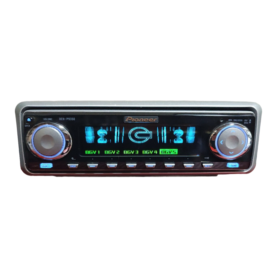
5/∞/2/3 buttons EJECT button BAND button SOURCE button Multi-function buttons BACK button NEXT button - DEH-P930/UC, DEH-P9300/UC ATT button This lets you quickly lower volume level (by about 90%). Press once more to return to the original volume level. BAND button... - Page 83 DEH-P930,P9300,P9350 - DEH-P9350/ES ATT button This lets you quickly lower volume level (by about 90%). Press once more to return to the original volume level. VOLUME Raise or lower the volume. 5/∞ buttons PGM button BAND button FUNCTION button AUDIO button...
- Page 84 DEH-P930,P9300,P9350...
- Page 85 DEH-P930,P9300,P9350...
- Page 86 DEH-P930,P9300,P9350...
- Page 87 DEH-P930,P9300,P9350...
- Page 88 DEH-P930,P9300,P9350...
- Page 89 DEH-P930,P9300,P9350...
-
Page 90: Specifications
Load impedance ......4 Ω (4 – 8 Ω allowable) Preout maximum output level/ Frequency range ........87.5 – 108 MHz output impedance (DEH-P930/UC) ..6.5 V/100 Ω Usable sensitivity ............9 dBf output impedance (DEH-P9300/UC) ..4.0 V/100 Ω...
Need help?
Do you have a question about the DEH-P9350 and is the answer not in the manual?
Questions and answers