Table of Contents
Advertisement
S
ervice
M anua l
MULTI-CD/MD/DAB CONTROL DSP HIGH POWER CD PLAYER WITH RDS TUNER
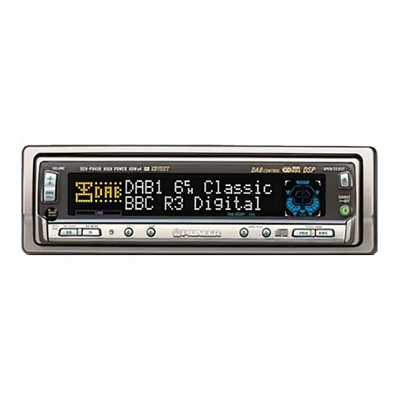
DEH-P945R
MULTI-CD/MD/DAB CONTROL DSP CD PLAYER WITH RDS TUNER
DEX-P99R
- See the separate manual CX-680(CRT2216) for the CD mechanism description, disassembly and circuit
description.
- The CD mechanism employed in this model is one of H1 series.
CONTENTS
1. SAFETY INFORMATION ............................................2
2. EXPLODED VIEWS AND PARTS LIST .......................3
3. SCHEMATIC DIAGRAM ...........................................16
4. PCB CONNECTION DIAGRAM ................................46
5. ELECTRICAL PARTS LIST ........................................64
6. ADJUSTMENT..........................................................79
PIONEER ELECTRONIC CORPORATION
PIONEER ELECTRONICS SERVICE INC.
PIONEER ELECTRONIC [EUROPE] N.V.
PIONEER ELECTRONICS ASIACENTRE PTE.LTD. 501 Orchard Road, #10-00, Wheelock Place, Singapore 238880
C PIONEER ELECTRONIC CORPORATION 1998
DEH-P945R/EW
4-1, Meguro 1-Chome, Meguro-ku, Tokyo 153-8654, Japan
P.O.Box 1760, Long Beach, CA 90801-1760 U.S.A.
Haven 1087 Keetberglaan 1, 9120 Melsele, Belgium
EW
7. GENERAL INFORMATION .......................................83
7.1 PARTS .................................................................83
7.1.1 IC................................................................83
7.1.2 DISPLAY ..................................................100
7.2 DIAGNOSIS ......................................................101
7.2.1 DISASSEMBLY .......................................101
7.2.2 TEST MODE ............................................102
7.3 BLOCK DIAGRAM ............................................108
8. OPERATIONS AND SPECIFICATIONS...................110
K-FEA. JUNE 1998 Printed in Japan
ORDER NO.
CRT2207
EW
Advertisement
Table of Contents

Related Manuals for Pioneer DEH-P945R


Summary of Contents for Pioneer DEH-P945R
-
Page 1: Table Of Contents
P.O.Box 1760, Long Beach, CA 90801-1760 U.S.A. PIONEER ELECTRONIC [EUROPE] N.V. Haven 1087 Keetberglaan 1, 9120 Melsele, Belgium PIONEER ELECTRONICS ASIACENTRE PTE.LTD. 501 Orchard Road, #10-00, Wheelock Place, Singapore 238880 C PIONEER ELECTRONIC CORPORATION 1998 K-FEA. JUNE 1998 Printed in Japan... -
Page 2: Safety Information
DEH-P945R,DEX-P99R - CD Player Service Precautions 2. During disassembly, be sure to turn the power off 1. For pickup unit(CXX1290) handling, please refer since an internal IC might be destroyed when a con- to"Disassembly"(CX-680 Service Manual CRT2216). nector is plugged or unplugged. -
Page 3: Exploded Views And Parts List
DEH-P945R,DEX-P99R 2. EXPLODED VIEWS AND PARTS LIST 2.1 PACKING 34 34... - Page 4 DEH-P945R,DEX-P99R NOTE: - Parts marked by "*"are generally unavailable because they are not in our Master Spare Parts List. ∇ mark on the product are used for disassembly. - Screws adjacent to - PACKING SECTION PARTS LIST (1) PARTS LIST Mark No.
- Page 5 DEH-P945R/EW, DEX-P99R/EW CRD2655 English, Spanish CRD2656 German, French CRD2657 Italian, Dutch (2) CONTRAST TABLE DEH-P945R/EW and DEX-P99R/EW are constructed same except for the following: Part No. Mark No. Symbol and Description DEH-P945R/EW DEX-P99R/EW 20 Carton CHG3534 CHG3533 28 Cord Assy...
- Page 6 DEH-P945R,DEX-P99R 2.2 EXTERIOR (1) - DEH-P945R/EW 79 97...
- Page 7 DEH-P945R,DEX-P99R - EXTERIOR (1) SECTION PARTS LIST Mark No. Description Part No. Mark No. Description Part No. 1 Screw BSZ26P050FMC 46 Plug(CN451,804) CKS1222 2 Screw BSZ30P055FMC 47 ••••• 3 Cord Assy CDE5785 48 Plug(CN803) CKS1225 4 Cord CDE5536 49 Connector(CN801)
- Page 8 DEH-P945R,DEX-P99R Mark No. Description Part No. Mark No. Description Part No. 91 Gear CNV5273 116 Battery Cover CNS5032 92 Rack CNV5274 CXK5101 CD Mechanism Module(H1) 93 Lighting Conductor CNV5276 118 Chassis Unit CXB2229 94 Guide CNV5356 119 Switch(S951) CSN1012 95 Gathering PCB...
- Page 9 DEH-P945R,DEX-P99R - DEX-P99R/EW 79 97 160 160 45 50...
- Page 10 DEH-P945R,DEX-P99R - EXTERIOR (1) SECTION PARTS LIST Mark No. Description Part No. Mark No. Description Part No. 1 Screw BSZ26P050FMC 46 Plug(CN451,804) CKS1222 2 Screw BSZ30P055FMC 47 ••••• 3 Cord Assy CDE5785 48 Plug(CN803) CKS1225 4 Cord CDE5536 49 Connector(CN801)
- Page 11 DEH-P945R,DEX-P99R Mark No. Description Part No. Mark No. Description Part No. 91 Gear CNV5273 126 ••••• 92 Rack CNV5274 127 Handle CNC5395 93 Lighting Conductor CNV5276 128 Spring CBH-865 94 Guide CNV5356 129 Bush CNV1917 95 Gathering PCB CNX2961 130 Holder...
- Page 12 9 Holder CNC7547 19 Button CAC5491 10 LCD(LCD1901) See Contrast table(2) (2) CONTRAST TABLE DEH-P945R/EW and DEX-P99R/EW are constructed same except for the following: Part No. Mark No. Symbol and Description DEH-P945R/EW DEX-P99R/EW 1 Grille Unit CXB2203 CXB2202 8 Keyboard Unit...
- Page 13 DEH-P945R,DEX-P99R...
- Page 14 DEH-P945R,DEX-P99R 2.4 CD MECHANISM MODULE...
- Page 15 DEH-P945R,DEX-P99R - CD MECHANISM MODULE SECTION PARTS LIST Mark No. Description Part No. Mark No. Description Part No. 1 Control Unit CWX2166 51 Spring CBH2039 2 Connector(CN701) CKS1968 52 Lack CNV5471 3 Connector(CN802) CKS3477 53 Bracket Unit CXB1674 4 Connector(CN801)
-
Page 16: Schematic Diagram
DEH-P945R,DEX-P99R 3. SCHEMATIC DIAGRAM 3.1 OVERALL CONNECTION DIAGRAM(GUIDE PAGE) Note: When ordering service parts, be sure to refer to “EXPLODED VIEWS AND PARTS LIST” or “ELECTRICAL PARTS LIST”. Large size CD MECHANISM MODULE M.CD:+2.2dBs SCH diagram Guide page M.CD:+2.2dBs 4.1V FM100%:-16.0dBs... - Page 17 DEH-P945R,DEX-P99R TUNER AMP UNIT DEH-P945R/EW ONLY DEX-P99R/EW ONLY E G H M.CD:+37.1dBs FM100%:+35.15dBs AM30%:-25.15dBs R237-242 DEH-P945R/EW:22K DEX-P99R/EW:11K CN3001 DEH-P945R/EW ONLY DEX-P99R/EW ONLY CEK1136 CEK1089 0.5A CEK1089 0.5A C943:47/10(DEH-P945R/EW) :47/25(DEX-P99R/EW) DEX-P99R/EW ONLY DEH-P945R/EW ONLY...
- Page 18 DEH-P945R,DEX-P99R...
- Page 19 DEH-P945R,DEX-P99R...
- Page 20 DEH-P945R,DEX-P99R...
- Page 21 DEH-P945R,DEX-P99R...
- Page 22 DEH-P945R,DEX-P99R 3.2 CD MECHANISM MODULE(GUIDE PAGE) Large size SCH diagram Guide page Detailed page D I J...
- Page 23 DEH-P945R,DEX-P99R...
- Page 24 DEH-P945R,DEX-P99R...
- Page 25 DEH-P945R,DEX-P99R...
- Page 26 DEH-P945R,DEX-P99R...
- Page 27 DEH-P945R,DEX-P99R...
- Page 28 DEH-P945R,DEX-P99R Note:1. The encircled numbers denote measuring pointes in the circuit diagram. 2. Reference voltage - Waveforms REFO:2.5V 1 RFO 1 CH1: RFO 1 CH1: RFO 0.5V/div. 0.5µs/div. 1V/div. 1V/div. 0.5ms/div. 0.5ms/div. 2 CH2: MIRR 2 CH2: MIRR Normal mode: play 5V/div.
- Page 29 DEH-P945R,DEX-P99R 8 CH1: TEY 8 CH1: TEY 0 SIN 0.2V/div. 0.5V/div. 0.5V/div. 0.1s/div. 5ms/div. 20ms/div. 9 CH2: TIN ! CH2: SD 0.2V/div. 0.5V/div. Normal mode: play Normal mode: Play (12cm) → REFO → REFO → REFO → → REFO REFO...
- Page 30 DEH-P945R,DEX-P99R ( CH1: R OUT 6 CH1: FEY 8 CH1: TEY 0.2V/div. 1V/div. 0.2V/div. 0.2ms/div. 1ms/div. 1ms/div. ) CH2: L OUT 3 CH2: FIN 9 CH2: TIN 1V/div. 0.5V/div. 0.5V/div. Normal mode: Play (1kHz 0dB) Normal mode: During AGC Normal mode: During AGC →...
- Page 31 DEH-P945R,DEX-P99R...
- Page 32 DEH-P945R,DEX-P99R 3.3 FM/AM TUNER UNIT...
- Page 33 DEH-P945R,DEX-P99R...
- Page 34 DEH-P945R,DEX-P99R 3.4 KEYBOARD PCB S1911:CSG1084 (DEH-P945R/EW) :CSG1107 (HEX-P99R/EW) S1915:CSG1085 (DEH-P945R/EW) :CSG1108 (DEX-P99R/EW)
- Page 35 DEH-P945R,DEX-P99R KEYBOARD PCB LCD1901 CAW1471 (DEH-P945R/EW) CAW1493 (DEX-P99R/EW)
- Page 36 DEH-P945R,DEX-P99R 3.5 DSP UNIT(GUIDE PAGE) Large size SCH diagram M.CD:+4.5dBs FM100%:+2.55dBs Guide page AM30%:-7.45dBs Detailed page CN222...
- Page 37 DEH-P945R,DEX-P99R :ANALOG AUDIO INPUT :DIGITAL AUDIO :FRONT AUDIO OUTPUT (Front/Miid) :FRONT AUDIO DIGITAL :REAR AUDIO OUTPUT (Rear/Hi) :REAR AUDIO DIGITAL :SUBWOOFER AUDIO OUTPUT :SUBWOOFER AUDIO DIGITAL (Sub.w/Low) DSP UNIT (DEH-P945R/EW) M.CD:+11.1dBs FM100%:+4.55dBs AM30%:-5.45dBs (DEX-P99R/EW) M.CD:+6.5dBs FM100%:+4.55dBs AM30%:-5.45dBs M.CD:+1.5dBs(DEH-P945R/EW) M.CD:+2.1dBs(DEX-P99R/EW) FM100%:-0.45dBs AM30%:-10.45dBs...
- Page 38 DEH-P945R,DEX-P99R...
- Page 39 DEH-P945R,DEX-P99R...
- Page 40 DEH-P945R,DEX-P99R...
- Page 41 DEH-P945R,DEX-P99R...
- Page 42 DEH-P945R,DEX-P99R 3.6 ASL UNIT...
- Page 43 DEH-P945R,DEX-P99R 3.7 MICROPHONE JACK UNIT MICROPHONE JACK UNIT...
- Page 44 DEH-P945R,DEX-P99R 3.8 HIGH OUT UNIT (DEX-P99R/EW) M.CD:+13.72dBs FM100%:+11.77dBs AM30%:+1.77dBs CN4003 CN4002 CN4001 CN4004...
- Page 45 DEH-P945R,DEX-P99R 3.9 D/D CONVERTER UNIT (DEX-P99R/EW) D/D CONVERTER UNIT...
-
Page 46: Pcb Connection Diagram
DEH-P945R,DEX-P99R NOTE FOR PCB DIAGRAMS 1. The parts mounted on this PCB include all necessary parts for several destination. For further information for respective destinations, be sure to 4. PCB CONNECTION DIAGRAM check with the schematic diagram. CORD ASSY MAIN ANT. - Page 47 DEH-P945R,DEX-P99R 2. Viewpoint of PCB diagrams Capacitor Connector SIDE A SIDE A SIDE B Chip Part P.C.Board CN701 INVERTER ASSY CN1901...
- Page 48 DEH-P945R,DEX-P99R TUNER AMP UNIT...
- Page 49 DEH-P945R,DEX-P99R SIDE B...
- Page 50 DEH-P945R,DEX-P99R 4.2 FM/AM TUNER UNIT SIDE A...
- Page 51 DEH-P945R,DEX-P99R SIDE B...
- Page 52 DEH-P945R,DEX-P99R 4.3 CD MECHANISM MODULE SIDE A CONTROL UNIT...
- Page 53 DEH-P945R,DEX-P99R SIDE B CONTROL UNIT REFO PICKUP UNIT CN671 SPINDLE MOTOR CN221...
- Page 54 DEH-P945R,DEX-P99R...
- Page 55 DEH-P945R,DEX-P99R...
-
Page 56: Keyboard Unit
DEH-P945R,DEX-P99R 4.4 KEYBOARD UNIT KEYBOARD UNIT KEYBOARD UNIT CN801... - Page 57 DEH-P945R,DEX-P99R SIDE A SIDE B...
- Page 58 DEH-P945R,DEX-P99R 4.5 DSP UNIT SIDE A DSP UNIT...
- Page 59 DEH-P945R,DEX-P99R SIDE B DSP UNIT CN222...
- Page 60 DEH-P945R,DEX-P99R 4.6 ASL UNIT SIDE A ASL UNIT CN141 SIDE B ASL UNIT...
- Page 61 DEH-P945R,DEX-P99R 4.7 FLAP SENSE PCB, MICROPHONE JACK UNIT FLAP SENSE PCB CN852 SIDE A SIDE B MICROPHONE JACK UNIT MICROPHONE JACK UNIT CN131...
- Page 62 DEH-P945R,DEX-P99R 4.8 D/D CONVERTER UNIT, D/D CONVERTER PCB (DEX-P99R/EW) SIDE A SIDE B D/D CONVERTER UNIT D/D CONVERTER UNIT SIDE A SIDE B D/D CONVERTER PCB D/D CONVERTER PCB CN4004 CN4002 CN4003 CN251 CN4001...
- Page 63 DEH-P945R,DEX-P99R 4.9 HIGH OUT UNIT (DEX-P99R/EW) SIDE A HIGH OUT UNIT RCA OUT CN231 CN252 SIDE B HIGH OUT UNIT...
-
Page 64: Electrical Parts List
DEH-P945R,DEX-P99R 5. ELECTRICAL PARTS LIST NOTES: - Parts whose parts numbers are omitted are subject to being not supplied. - The part numbers shown below indicate chip components. Chip Resistor RS1/_S___J,RS1/__S___J Chip Capacitor (except for CQS..) CKS.., CCS.., CSZS..=====Circuit Symbol and No.===Part Name Part No. - Page 65 DEH-P945R,DEX-P99R =====Circuit Symbol and No.===Part Name Part No. =====Circuit Symbol and No.===Part Name Part No. ------ ------------------------------------------ ------------------------- ------ ------------------------------------------ ------------------------- CKSQYB104K16 CKSRYB332K50 CCSRCKR50C50 CKSQYB473K16 CEJA1R0M50 CCSRCH120J50 CKSRYB222K50 CKSRYB472K50 CCSRCH220J50 CEJAR47M50 CCSRCH8R0D50 CKSQYB104K16 CKSRYB222K50 CEJAR47M50 CKSRYB103K25 CEJAR33M50 CKSRYB222K50 CKSQYB473K16 CKSRYB222K50...
- Page 66 UN2212 CKSQYB334K16 Transistor 2SB1243 22µF/6.3V CCH1300 Transistor UN2212 Transistor UN2211 CEVL101M6R3 Transistor IMX1 CKSRYB221K50 Transistor 2SA1162 Unit Number : CWM5696(DEH-P945R/EW) Transistor 2SC2712 Unit Name : Tuner Amp Unit Transistor IMD2A Transistor 2SD2396 MISCELLANEOUS Diode MA3039(L) CA0008AM Diode MA152WA TA2050S Diode...
- Page 67 DEH-P945R,DEX-P99R =====Circuit Symbol and No.===Part Name Part No. =====Circuit Symbol and No.===Part Name Part No. ------ ------------------------------------------ ------------------------- ------ ------------------------------------------ ------------------------- Diode DA204K RS1/10S332J Diode DA204K RS1/10S562J Diode DA204K RS1/10S472J Diode DA204K RS1/10S103J Diode MA3062(M) RS1/10S223J Diode DA204K RS1/10S473J Diode...
- Page 68 DEH-P945R,DEX-P99R =====Circuit Symbol and No.===Part Name Part No. =====Circuit Symbol and No.===Part Name Part No. ------ ------------------------------------------ ------------------------- ------ ------------------------------------------ ------------------------- RS1/10S682J RS1/16S473J RS1/10S102J RS1/10S102J RS1/10S472J RS1/10S202J RS1/10S682J RA3C681J RS1/10S561J RS1/10S473J RS1/10S103J RS1/10S473J RS1/10S222J RS1/10S473J RS1/10S152J RS1/10S473J RS1/10S392J RS1/10S102J RS1/10S392J...
- Page 69 DEH-P945R,DEX-P99R =====Circuit Symbol and No.===Part Name Part No. =====Circuit Symbol and No.===Part Name Part No. ------ ------------------------------------------ ------------------------- ------ ------------------------------------------ ------------------------- RD1/4PU561J CCSQCH390J50 RS1/10S102J CEJA1R0M50 RS1/10S102J CEJA220M6R3 RS1/10S102J CEJA101M10 RS1/10S102J CEJA100M16 RS1/10S473J CKSQYB223K50 RS1/10S473J CEJA4R7M35 RS1/10S0R0J CEJA4R7M35 RS1/10S102J CEJA100M16 RD1/4PU102J...
- Page 70 DEH-P945R,DEX-P99R =====Circuit Symbol and No.===Part Name Part No. =====Circuit Symbol and No.===Part Name Part No. ------ ------------------------------------------ ------------------------- ------ ------------------------------------------ ------------------------- CKSQYB471K50 CKSQYB105K10 CKSQYB103K50 CCSQCH101J50 CKSQYB223K50 CEJA2R2M50 CKSQYB103K50 CKSQYB102K50 CKSQYB223K50 CKSQYB104K16 CKSQYB223K50 CKSQYB473K16 CCSQCH270J50 CKSQYB102K50 CCSQCH270J50 CEJA101M10 CKSQYB103K50 CKSQYB103K50 Unit Number : CWM5695(DEX-P99R/EW)
- Page 71 DEH-P945R,DEX-P99R =====Circuit Symbol and No.===Part Name Part No. =====Circuit Symbol and No.===Part Name Part No. ------ ------------------------------------------ ------------------------- ------ ------------------------------------------ ------------------------- Transistor UN2212 Resonator 12.58291MHz CSS1402 Transistor 2SB1238 Resonator 4.19MHz CSS1436 Transistor DTC123EK Slide Switch(PRO/STD) CSH1048 Transistor 2SD1760F5 Lamp 14V40mA...
- Page 72 DEH-P945R,DEX-P99R =====Circuit Symbol and No.===Part Name Part No. =====Circuit Symbol and No.===Part Name Part No. ------ ------------------------------------------ ------------------------- ------ ------------------------------------------ ------------------------- RS1/10S223J RS1/10S0R0J RS1/10S331J RD1/4PU151J RS1/10S331J RS1/10S562J RS1/10S331J RS1/10S333J RS1/10S103J (RN1/10SE4702D) GGC1316 RS1/10S102J (RN1/10SE4702D) GGC1316 RS1/10S473J RS1/16S102J RS1/10S473J RS1/10S821J RS1/10S223J...
- Page 73 DEH-P945R,DEX-P99R =====Circuit Symbol and No.===Part Name Part No. =====Circuit Symbol and No.===Part Name Part No. ------ ------------------------------------------ ------------------------- ------ ------------------------------------------ ------------------------- RS1/10S272J CAPACITORS RS1/10S223J RS1/10S272J CKSQYB104K16 RS1/10S223J CKSQYB104K16 RS1/10S272J CEJA1R0M50 CEJA1R0M50 RS1/10S473J CEJA100M16 RS1/10S473J RS1/10S473J CEJA100M16 RS1/8S331J CEJA1R0M50 RS1/10S274J CEJA1R0M50...
- Page 74 CCSQCH270J50 CEJA2R2M50 CKSQYB103K50 CKSQYB102K50 CKSQYB103K50 CKSQYB104K16 CKSQYB472K50 CKSQYB473K16 CKSQYB104K16 CKSQYB102K50 CKSQYB105K10 CEJA101M10 CKSQYB104K16 CKSQYB222K50 Unit Number : CWM5688(DEH-P945R/EW) CCSQCH101J50 Unit Number : CWM5687(DEX-P99R/EW) CEJA100M16 Unit Name : Keyboard Unit CKSQYB223K50 MISCELLANEOUS CKSQYB104K16 CKSQYB223K50 IC 1901 HIC Module RS-140 CCSQCH200J50 IC 1902...
- Page 75 DEH-P945R,DEX-P99R =====Circuit Symbol and No.===Part Name Part No. =====Circuit Symbol and No.===Part Name Part No. ------ ------------------------------------------ ------------------------- ------ ------------------------------------------ ------------------------- 1920 CL170PGCD 1953 RS1/10S624J 1901 Chip Inductor LCTA2R2J3225 1954 RS1/10S471J 1902 Inductor LCTB2R2K2125 1955 RS1/10S471J 1903 Inductor LCTB2R2K2125 1956...
- Page 76 DEH-P945R,DEX-P99R =====Circuit Symbol and No.===Part Name Part No. =====Circuit Symbol and No.===Part Name Part No. ------ ------------------------------------------ ------------------------- ------ ------------------------------------------ ------------------------- 3152 High Loss Inductor CTF1410 3154 RSK1/16S151J 3153 High Loss Inductor CTF1410 3155 RSK1/16S151J 3154 High Loss Inductor CTF1410...
- Page 77 DEH-P945R,DEX-P99R =====Circuit Symbol and No.===Part Name Part No. =====Circuit Symbol and No.===Part Name Part No. ------ ------------------------------------------ ------------------------- ------ ------------------------------------------ ------------------------- 4506 RS1/8S682J 4018 (RN1/10SE1502D) GGC1322 4507 RS1/8S684J 4019 (RN1/10SE3002D) GGC1323 4508 RS1/8S562J 4509 RS1/8S391J CAPACITORS 4510 RS1/8S472J 4001 33µF/25V...
- Page 78 DEH-P945R,DEX-P99R =====Circuit Symbol and No.===Part Name Part No. ------ ------------------------------------------ ------------------------- CAPACITORS 4151 CEWAR100M50 4152 CKSQYB471K50 4153 CEWAR100M50 4154 CEWAR100M50 4157 CCSQCH820J50 4158 CCSQCH820J50 4253 CEWAR100M50 4254 CEWAR100M50 4257 CCSQCH820J50 4258 CCSQCH820J50 4353 CEWAR100M50 4354 CEWAR100M50 4357 CCSQCH820J50 4358 CCSQCH820J50...
-
Page 79: Adjustment
DEH-P945R,DEX-P99R 6. ADJUSTMENT 6.1 TUNER ADJUSTMENT - Connection Diagram BACK UP +14.4V DC Regulated Power Supply Lch + 4 Ω Lch - mV Meter (1) Oscilloscope Rch + 4 Ω Rch - Dummy Antenna Antenna Plug 50 Ω(37.5 Ω) Stereo... - Page 80 DEH-P945R,DEX-P99R FM ADJUSTMENT Modulation M:MONO MOD., 400Hz 30%(22.5kHz Dev.) S:STEREO MOD., 1kHz, L or R=30%(20.25kHz+7.5kHz Dev.) NOTE:Before proceeding to further adjustments after switching power ON, let the tuner run for ten minutes to allow the circuits to stabilize. FM SSG...
-
Page 81: Checking The Grating After Changing The Pickup Unit
DEH-P945R,DEX-P99R 6.3 CHECKING THE GRATING AFTER CHANGING THE PICKUP UNIT • Note : Unlike previous CD mechanism modules the grating angle of the PU unit cannot be adjusted after the PU unit is changed. The PU unit in the CD mechanism module is adjusted on the production line to match the CD mecha- nism module and is thus the best adjusted PU unit for the CD mechanism module. - Page 82 DEH-P945R,DEX-P99R Ech → Xch 20mV/div, AC Grating waveform Fch → Ych 20mV/div, AC 0° 30° 45° 60° 75° 90°...
-
Page 83: General Information
DEH-P945R,DEX-P99R 7. GENERAL INFORMATION 7.1 PARTS 7.1.1 IC UPD63702AGF PD4931A GGC1325(M5M51016BTP-70LL) BA6797FM PD0236AM TC7S08FU LC89170M PD6237B AK4321VF BA05SFP SED1540F0A PM0017AM LB1930M SED1526F0A NJM4580M PM2007A PD5445A PD4905A AK7712AVT - Pin Functions (UPD63702AGF) Pin No. Pin Name Function and Operation D.VDD Supplies current of positive voltage to the logic circuits... - Page 84 DEH-P945R,DEX-P99R Pin No. Pin Name Function and Operation LOCK Indicates "H" when the synchronized pattern detection signal matches the frame counter output at the EFM recovery modulation, and "L" when they don't match WFCK Minute-cycle signal for the bit clock, the signal indicates the cycle of 1 frame (approx.
- Page 85 DEH-P945R,DEX-P99R - Pin Functions (BA6797FM) Pin No. Pin Name Function and Operation OUT1-A Driver CH1 output OUT1-B Driver CH1 output PRE-OUT1 CH1 pre-amplifier output IN1(-) CH1 pre-amplifier inverted input IN1(+) CH1 pre-amplifier input REG-B External Tr base connection REG-OUT Fixed voltage output (External Tr collect connection)
- Page 86 DEH-P945R,DEX-P99R IC702:BA05SFP LB1930M OUT1 OUT2 P-GND S-GND PM2007A...
- Page 87 DEH-P945R,DEX-P99R - Pin Functions (PD4905A) Pin No. Pin Name Function and Operation swvdd GRIL:Power Output dsens Detach sense input psens Grille eject button sense input isens Illumination sense input TESTIN Test program input drst Reset output Not used SK input...
- Page 88 DEH-P945R,DEX-P99R Pin No. Pin Name Function and Operation bsrqc P-BUS:Communication request input (CD) bsck P-BUS:Data clock input/output (Test mode clock output) P-BUS:Communication data input (Test mode data input) P-BUS:Communication data output brst P-BUS:Reset output MICSEL Mic select output bsrqd P-BUS:Communication request input (DSP)
- Page 89 DEH-P945R,DEX-P99R - Pin Functions (PD4931A) Pin No. Pin Name Format Function and Operation Focus OK input MIRR Mirror detect input LOCK Spindle lock input AVss A/D GND electric potential Not used EMPH Pre-emphasis output AVREF1 A/D Reference electric potential input...
- Page 90 DEH-P945R,DEX-P99R Pin No. Pin Name Format Function and Operation VDSENS VD short sense input TEMP Temperature sense input Not used Format Meaning C MOS *PD4931A - Pin Functions (PD0236AM) Pin No. Pin Name Function and Operation BCSEL Bit clock fs select...
- Page 91 DEH-P945R,DEX-P99R - Pin Functions (PD6237B) Pin No. Pin Name Format Function and Operation Not used Address bus read strobe output Digital GND Address bus write strobe output 13-18 Not used KYDT Key data to system micro-computer DPDT Display data from system micro-computer...
- Page 92 DEH-P945R,DEX-P99R - Pin Functions (SED1540F0A) Pin No. Pin Name Function and Operation 1-72 SEG71-0 Output for driving segment of LC Normally the lowest bit in the address bus of MPU is connected to distinguish between data and command. 74,75 OSC1,2...
- Page 93 DEH-P945R,DEX-P99R - Pin Functions (SED1526F0A) Pin No. Pin Name Function and Operation V1-V5 Multilevel power supply for driving LCD Voltage adjustment +5V power supply VOUT Ascending voltage output CAP2- Ascending voltage capacitor connection CAP2+ Not used CAP1- Ascending voltage capacitor connection...
- Page 94 DEH-P945R,DEX-P99R - Pin Functions (PD5445A) Pin No. Pin Name Format Function and Operation SPCK Connect to GND Not used Electronic volume strobe output Electronic volume data output Electronic volume clock output CNVss Connect to Vss MCKRQ CD unit MCK request input...
- Page 95 DEH-P945R,DEX-P99R Pin No. Pin Name Format Function and Operation LRCKK LRCK/BCLK select SDATAK Audio data select:LRCKK inverted gate NOISE ASL noise input AVss Connect Vss MCKOUT CD MCLK gate control Vref AD select reference voltage input AVcc Connect to Vcc...
- Page 96 DEH-P945R,DEX-P99R - Pin Functions (AK7712AVT) Pin No. Pin Name Function and Operation TSTI1 Test input 1 OPCL ADC,DAC connection select pdad AD reset control pdda DA reset control Power down Reset input TSTIO1 Test input/output 1 TSTIO2 Test input/output 2...
- Page 97 DEH-P945R,DEX-P99R Pin No. Pin Name Function and Operation AOUTR1 DAC1 Rch analog output 1 AOUTL1 DAC1 Lch analog output 1 VRDAL DAC reference voltage input AVSS Analog GND AVDD Analog power supply VRDAH DAC reference voltage input Not used AINR-...
- Page 98 DEH-P945R,DEX-P99R TC7S08FU 1 IN B 5 VCC 2 IN A 3 GND 4 OUT Y AK4321VF...
- Page 99 DEH-P945R,DEX-P99R - Pin Functions (PM0017AM) Pin No. Pin Name Function and Operation AGND Analog GND vref Reference voltage noise cut IN1-6 CH1-6 input 9,10 Not used Terminal to set forced switching time DGND Digital GND Strobe input Clock input DATA...
-
Page 100: Display
DEH-P945R,DEX-P99R 7.1.2 DISPLAY - CAW1471 (DEH-P945R/EW) - CAW1493 (DEX-P99R/EW) -
Page 101: Diagnosis
DEH-P945R,DEX-P99R 7.2 DIAGNOSIS 7.2.1 DISASSEMBLY - Removing the Case,Panel and - Removing the Panel Assy CD Mechanism Module 1. A × 2 2. B × 2 1. A × 2 3. Connector × 4 2. Stopper × 5 4. Stopper × 2 3. -
Page 102: Test Mode
DEH-P945R,DEX-P99R 7.2.2 TEST MODE - CD Test Mode 1)Precautions • Test mode cancellation • This unit uses a single power supply (+5V) for the reg- Switch ACC, back-up OFF. ulator. The signal reference potential, therefore, is connected to REFO(approx. 2.5V) instead of GND. - Page 103 DEH-P945R,DEX-P99R - S-MD Test Mode This mode is used by service personnel to solve problems when the mechanism is malfunctioned. Normally users do not enter S-MD Test mode. (1) Test mode input 1) How to input Input in the same manner as with inputting in Test mode of CDS, CDM, etc.
- Page 104 DEH-P945R,DEX-P99R - Flow Chart TR - ACC,Back-up ON Regulator OFF CD Player Select SOURCE During regulator off, press the 6 key and the system will be put into the Display new test mode. Regulator ON BAND Power ON TRK 00...
- Page 105 DEH-P945R,DEX-P99R - Error Number Indication The system enters error mode to display the cause of error with a number when the system cannot operate CD or stops operation because of an error. The purpose of this measure is to reduce frequency of calls from users asking help for problems that are caused by incorrect operation by user, as well as to assist analysis and repair in servicing.
- Page 106 DEH-P945R,DEX-P99R - New Test Mode When S-CD is specified as the source, basically the system plays as normal operation. After setup, the system dis- plays the cause and time (absolute time) of an error if focus search is improper, spindle lock is removed, subcode cannot be read, or sound is skipped.
- Page 107 DEH-P945R,DEX-P99R...
-
Page 108: Block Diagram
DEH-P945R,DEX-P99R 7.3 BLOCK DIAGRAM - DEH-P945R/EW TUNER AMP UNIT ASL UNIT Q4501 VR4501 ASL AMP ASL FILTER MIC4501 CN141 IC4501 IC4502 NOISE NJM2068 NJM2068 CN451 MAIN Q403 FM / AM TUNER UNIT 26 25 Q31 CF51 CF52 CF53 FM MIX... - Page 109 DEH-P945R,DEX-P99R DSP UNIT CN231 N141 FRONT Lch OISE SWITCH SWITCH CN222 CN3001 CN3001 CD DATA Q231 BICK IC3142 LRCK TC7S08FU REAR Lch LRCK BICK IC3141 BU4066BCFV Q232 9 10 SUB.W Lch A OUT L1 Q233 AOUTL1 IC3201 BICK BICK PE2001AF...
-
Page 110: Operations And Specifications
DEH-P945R,DEX-P99R 8. OPERATIONS AND SPECIFICATIONS 8.1 OPERATIONS... - Page 111 DEH-P945R,DEX-P99R...
- Page 112 DEH-P945R,DEX-P99R...
- Page 113 DEH-P945R,DEX-P99R...
- Page 114 DEH-P945R,DEX-P99R...
- Page 115 DEH-P945R,DEX-P99R...
- Page 116 DEH-P945R,DEX-P99R...
- Page 117 DEH-P945R,DEX-P99R...
- Page 118 DEH-P945R,DEX-P99R...
- Page 119 DEH-P945R,DEX-P99R...
- Page 120 DEH-P945R,DEX-P99R...
- Page 121 DEH-P945R,DEX-P99R...
- Page 122 DEH-P945R,DEX-P99R...
- Page 123 DEH-P945R,DEX-P99R...
- Page 124 DEH-P945R,DEX-P99R...
- Page 125 DEH-P945R,DEX-P99R...
- Page 126 DEH-P945R,DEX-P99R...
- Page 127 DEH-P945R,DEX-P99R...
- Page 128 DEH-P945R,DEX-P99R...
- Page 129 DEH-P945R,DEX-P99R...
- Page 130 DEH-P945R,DEX-P99R...
- Page 131 DEH-P945R,DEX-P99R...
- Page 132 DEH-P945R,DEX-P99R...
Need help?
Do you have a question about the DEH-P945R and is the answer not in the manual?
Questions and answers