Sony DVP-FX930 Service Manual
Portable cd/dvd player
Hide thumbs
Also See for DVP-FX930:
- Operating instructions manual (216 pages) ,
- Specification sheet (2 pages) ,
- Service manual (39 pages)
Table of Contents
Advertisement
DVP-FX930/FX930CC/FX930WM
SERVICE MANUAL
Ver. 1.0 2008.12
System
Laser: Semiconductor laser
Signal format system: NTSC
Inputs/Outputs
VIDEO (video input/output):
AUDIO (audio input/output)
PHONES (headphones) A/B:
Liquid Crystal Display
Panel size: 9 inches wide (diagonal)
Driving system: TFT active matrix
Resolution: 800 480 (effective pixel rate:
9-890-703-11
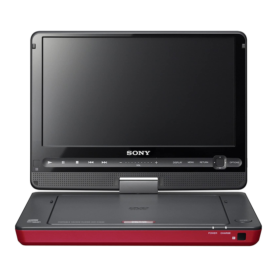
Photo: DVP-FX930
SPECIFICATIONS
Minijack
Output 1.0 Vp-p/75 ohms
Stereo minijack
Output 2.0 Vrms/47 kilohms
Recommended load impedance over
47 kilohms
Stereo minijack
more than 99.99%)
Sony Corporation
Video Business Group
General
Power requirements:
DC 9.5 V (AC power Adaptor/Car battery
adaptor)
DC 7.4 V (Battery pack)
Power consumption (DVD VIDEO Playback):
8.5 W (when used with a headphone)
Dimensions (approx.):
3
227 34.4 170.8 mm (9 1
/
8
3
6
/
4
inches) (width/height/depth) incl.
projecting parts
Mass (approx.): 900 g (1.98 lbs)
Operating temperature: 5 C to 35 C (41°F to
95°F)
Operating humidity: 25 % to 80 %
AC Power Adaptor: 110-240 V AC, 50/60 Hz
Car Battery Adaptor: 12 V DC
Supplied accessories
• Battery pack (NP-FX110) (1)
• AC power adaptor (1)
• Car battery adaptor (1)
• Audio/video cord (mini plug
2
phono plug 3) (1)
• Remote (with battery) (1)
Specifications and design are subject to change
without notice.
PORTABLE CD/DVD PLAYER
Published by Quality Assurance Dept.
RMT-D191
US Model
2008L0500-1
© 2008.12
Advertisement
Chapters
Table of Contents
Troubleshooting

Related Manuals for Sony DVP-FX930


Summary of Contents for Sony DVP-FX930
- Page 1 DVP-FX930/FX930CC/FX930WM RMT-D191 SERVICE MANUAL US Model Ver. 1.0 2008.12 Photo: DVP-FX930 SPECIFICATIONS General System Power requirements: Laser: Semiconductor laser DC 9.5 V (AC power Adaptor/Car battery Signal format system: NTSC adaptor) Inputs/Outputs DC 7.4 V (Battery pack) VIDEO (video input/output): Power consumption (DVD VIDEO Playback): 8.5 W (when used with a headphone)
- Page 2 THE PARTS LIST ARE CRITICAL TO SAFE OPERATION. RE- It is best to use only unleaded solder but unleaded solder may PLACE THESE COMPONENTS WITH SONY PARTS WHOSE also be added to ordinary solder. PART NUMBERS APPEAR AS SHOWN IN THIS MANUAL OR IN SUPPLEMENTS PUBLISHED BY SONY.
-
Page 3: Table Of Contents
DVP-FX930/FX930CC/FX930WM TABLE OF CONTENTS Section Title Page Section Title Page DISASSEMBLY WAVEFORMS AND CIRCUIT VOLTAGE 1-1. Disassembly Flow ............1-1 5-1. Waveforms ..............5-1 1-2. Bottom Block ..............1-1 5-2. Circuit Voltage Chart ............ 5-3 1-3. MAIN Board ..............1-2 1-4. -
Page 4: Disassembly
DVP-FX930/FX930CC/FX930WM SECTION 1 DISASSEMBLY • This set can be disassembled in the order shown below. 1-1. DISASSEMBLY FLOW 2-2. BOTTOM BLOCK 2-4. MONITOR SUB ASSY (Page 2-1) (Page 2-2) 2-2. MAIN BOARD 2-5. LCD (Page 2-2) (Page 2-3) Note: Follow the disassembly procedure in the numerical order given. -
Page 5: Main Board
DVP-FX930/FX930CC/FX930WM 1-3. MAIN BOARD 5 travers unit 4 flexible board 3 FFC 6 three screws (TS2 × 4.5) 2 connector 1 tape 7 main board 1-4. MONITOR SUB ASSY 6 housing cover assy 9 monitor sub assy 4 two screws (TS1.7 ×... -
Page 6: Lcd
DVP-FX930/FX930CC/FX930WM 1-5. qs two screws (TS1.7 × 5) qd panel brac L 4 six screws (TS1.7 × 5) 9 panel brac L-L 8 screw 2 LCD connector (TS1.7 × 5) 3 10 pin FFC 5 LCD board 6 screw (TS1.7 × 5) 7 panel brac L-R 0 two screws (TS1.7 ×... -
Page 7: Block Diagram
DVP-FX930/FX930CC/FX930WM SECTION 2 BLOCK DIAGRAM 2-1. OVERALL BLOCK DIAGRAM LCD BOARD KEY BOARD BackLight G Signal I2C Bus 9"PANEL MST7915MC VIDEO KEYPAD TFT-LCD DRIVER PROCESSING DIGITAL I2C Bus USB Unit RF Amp Y,C Out SWITCH CVBS Out/In Signal CVBS Out... -
Page 8: Schematic Diagrams
DVP-FX930/FX930CC/FX930WM SECTION 3 SCHEMATIC DIAGRAMS 3-1. FRAME SCHEMATIC DIAGRAM (1/2) -
Page 9: Frame Schematic Diagram (2/2)
DVP-FX930/FX930CC/FX930WM 3-2. FRAME SCHEMATIC DIAGRAM (2/2) -
Page 10: Main Board (1/5) (Dc-Dc Power)
DVP-FX930/FX930CC/FX930WM 3-3. MAIN BOARD (1/5) (DC-DC POWER) • See page 4-1 for printed wiring board. MAIN BOARD (1/5) ADVCC 330R 330R ADVCC ADVCC BAT_A DV33 BAT_A BAT_B CF12V3T3R00-3A32V CF12V3T3R00-3A32V BAT_B BTVCC LED1 LED1 BAT_C POWER BAT_C GREEN GREEN CHARGE_LED CHARGE_LED... - Page 11 DVP-FX930/FX930CC/FX930WM 3-4. MAIN BOARD (2/5) (DVD SERVO & DSP MT1389LP) • See page 4-1 for printed wiring board. MAIN BOARD (2/5) DV33 RFVDD3 RFV18 L3,L5 AADVDD DV33 RFV33 10uH/100mA 10uH/100mA AVCC 10uH/100mA 10uH/100mA ADACVDD Very Important to ADACVDD reduce Noise...
- Page 12 DVP-FX930/FX930CC/FX930WM 3-5. MAIN BOARD (3/5) (SDRAM & S-FLASH ROM) • See page 4-1 for printed wiring board. MAIN BOARD (3/5) 33R 0402 33R 0402 33R 0402 33R 0402 33R 0402 33R 0402 33R 0402 33R 0402 DCLK DCLK 33R 0402...
-
Page 13: Main Board (2/5) (Dvd Servo & Dsp Mt1389Lp)
DVP-FX930/FX930CC/FX930WM 3-6. MAIN BOARD (4/5) (VIDEO OUT & PANEL CONNECT) • See page 4-1 for printed wiring board. MAIN BOARD (4/5) SPR2 FB17 FB17 600R/400mA 600R/400mA USBM SPR1 FB14 FB14 600R/400mA 600R/400mA USBM USBP SPL1 FB23 FB23 600R/400mA 600R/400mA USBP... -
Page 14: Main Board (3/5) (Sdram & S-Flash Rom)
DVP-FX930/FX930CC/FX930WM 3-7. MAIN BOARD (5/5) (AUDIO) • See page 4-1 for printed wiring board. MAIN BOARD (5/5) AUDIO_VCC DC_IN DV33 AGND AOUT_L AOUT_L AOUT_R AUDIO_VCC +5VOP AOUT_R EC20 EC20 R149 R149 R150 R150 R151 R151 FB27 FB27 RLINE R_MUTE 1N4148... -
Page 15: Lcd Board (T_Con)
DVP-FX930/FX930CC/FX930WM 3-8. LCD BOARD (T_CON) • See page 4-3 for printed wiring board. LCD BOARD R1 10R R1 10R AGND IR_IN AGND AGND LED+ R3 1.5K R3 1.5K LED+ LED+ LED- LED- LED- PGND PGND PGND C_IN C_IN C_IN 100pF... -
Page 16: Key Board (Touch Board)
DVP-FX930/FX930CC/FX930WM 3-9. KEY BOARD (TOUCH BOARD) • See page 4-4 for printed wiring board. KEY BOARD DV33 10uf /6.3V 10uf /6.3V 1.8R/1206 1.8R/1206 SPR2 SPEAKER SPR1 1.8R/1206 1.8R/1206 SPL2 SPEAKER SPL1 DV33 TOUCH_PAD2 TOUCH_PAD9 100pf/NC 100pf/NC 100pf/NC 100pf/NC 100pf/NC 100pf/NC... -
Page 17: Printed Wiring Boards
DVP-FX930/FX930CC/FX930WM SECTION 4 PRINTED WIRING BOARDS 4-1. MAIN BOARD (SIDE A) • See page 1-6 for circuit boards location. There are a few cases that the part isn’t mounted in this model is printed on this diagram. : Uses unleaded solder. -
Page 18: Main Board (Side B)
DVP-FX930/FX930CC/FX930WM 4-2. MAIN BOARD (SIDE B) • See page 1-6 for circuit boards location. : Uses unleaded solder. MAIN BOARD (SIDE B) DC IN 9.5V – VIDEO AUDIO PHONES HOLD . POWER CHARGE POWER... -
Page 19: Lcd Board
DVP-FX930/FX930CC/FX930WM 4-3. LCD BOARD • See page 1-6 for circuit boards location. There are a few cases that the part isn’t mounted in this model is printed on this diagram. : Uses unleaded solder. LCD BOARD (SIDE A) LCD BOARD (SIDE B) -
Page 20: Key Board
DVP-FX930/FX930CC/FX930WM 4-4. KEY BOARD • See page 1-6 for circuit boards location. There are a few cases that the part isn’t mounted in this model is printed on this diagram. : Uses unleaded solder. KEY BOARD (SIDE A) KEY BOARD (SIDE B) >... -
Page 21: Waveforms And Circuit Voltage
DVP-FX930/FX930CC/FX930WM SECTION 5 WAVEFORMS AND CIRCUIT VOLTAGE 5-1. WAVEFORMS 1. Spindle control waveform (No disc condition) 2. Tracking control relate signal (system checking-cd) U (U8 PIN7) TRO (U6 PIN24) V (U8 PIN4) TRSO (R95) W (U8 PIN2) Fig 5-2 DMSO/ECR (U8 PIN21) 3. - Page 22 DVP-FX930/FX930CC/FX930WM 4. Audio output from IC (L/R) 5. Video output waveform (CVBS) DIN (U11 PIN6) AUDIO OUT (J6 PIN2) Fig 5-5 Fig 5-4 6. Video output waveform (Y/C) 7. RF waveform Y (FB218) DVDRFIP (U6 PIN12) C (FB16) Fig 5-6...
-
Page 23: Circuit Voltage Chart
DVP-FX930/FX930CC/FX930WM 5-2. CIRCUIT VOLTAGE CHART U6 (MT1389LP) U6 (MT1389LP) U6 (MT1389LP) U6 (MT1389LP) STOP (V) PLAY (V) STOP (V) PLAY (V) STOP (V) PLAY (V) STOP (V) PLAY (V) 2.038 2.136 0.011 0.011 2.569 2.504 2.039 2.149 2.984 2.981 1.414 1.435... - Page 24 DVP-FX930/FX930CC/FX930WM U9 (SDRAM) U9 (SDRAM) U7 (BA5954) U11 (PT2328) U14 (APA2068KA) U8 (6849/6869) STOP (V) PLAY (V) STOP (V) PLAY (V) STOP (V) PLAY (V) STOP (V) PLAY (V) STOP (V) PLAY (V) STOP (V) PLAY (V) 1.413 1.436 3.23 3.228...
-
Page 25: Ic Pin Function Description
DVP-FX930/FX930CC/FX930WM SECTION 6 IC PIN FUNCTION DESCRIPTION 6-1. MPEG/DSP/RF PIN FUNCTIOM (MAIN BOARD U6: MT1389LP) Pin No. Name Description RFA Analog Input RF main beam input A RFB Analog Input RF main beam input B RFC Analog Input RF main beam input C... - Page 26 DVP-FX930/FX930CC/FX930WM Pin No. Name Description DVDSD18 1.8V power pin for internal digital circuitry DQM0 PD data mask 0 RD15 DRAM data 15 RD14 DRAM data 14 RD13 DRAM data 13 RD12 DRAM data 12 DVSS33 3.3V Ground pin for internal digital circuitry...
- Page 27 DVP-FX930/FX930CC/FX930WM Pin No. Name Description C single output CVBS 3.3V power pin AADVSS 3.3V power pin for audio clock circuitry AKIN2/GPIO19/ APLL external capacitance connection AUDIO_MUTE ADVCM/GPIO20/ Ground pin for audio DAC circuitry VCOM AKIN1/GPIO21/ Ground pin for audio DAC circuitry...
-
Page 28: Electrical Adjustment
DVP-FX930/FX930CC/FX930WM SECTION 7 ELECTRICAL ADJUSTMENT This section describes procedures and instructions necessary for 7-1. STANDARD VIDEO LEVEL adjusting electrical circuits in this set. 1. Checking Video Output Level Instruments required: <Purpose> 1) Color monitor TV This checks whether video output level satisfy the NTSC standard. -
Page 29: Troubleshooting
DVP-FX930/FX930CC/FX930WM SECTION 8 TROUBLESHOOTING 8-1. ELECTRICAL TROUBLE SHOOTING GUIDE 1. A. Power (DC-DC Converter) circuit No power on No power on by adaptor by battery Is adaptor Replace adaptor out 9.5V? Is battery OK? Replace battery Is P1 OK? Replace P1... -
Page 30: Yes No
DVP-FX930/FX930CC/FX930WM D. Video out abnormal E. Picture abnormal F. Disc error VIDEO OUT ABNORMAL PICTURE ABNORMAL DISC ERROR Check video jack J4 & mode Check the disc Check disc Check U11 filter Check the traverse Check traverse Check the U9 (SDRAM) - Page 31 DVP-FX930/FX930CC/FX930WM 2. MPEG Circuit Power is on Does logo appear Check power & clock on the screen? Does the moving picture Is MPEG data Check CD/DVD of the DVD disc play signal normal? DSP output signal on the screen normally?
-
Page 32: Replace Q2
DVP-FX930/FX930CC/FX930WM 3. Front Circuit START Power on Power Is DV33 OK? Check power green LED Do all Check the buttons work Replace U1 normally? Does Check remote remote control work Replace remote control control normally? Check DV33 Does IR1 work... - Page 33 DVP-FX930/FX930CC/FX930WM 4. RF/Servo Circuit No disc Put disc in? Check the RF Check the related connection between HA1 Disc ID is correct? circuit on U6 (MT1389LP) U6 (MT1389LP) RF signal Proper Does Check DMSO related DMSO signal on spindle circuit on U6 (MT1389LP)
-
Page 34: Lcd Trouble Shooting Guide
DVP-FX930/FX930CC/FX930WM 8-2. LCD TROUBLE SHOOTING GUIDE Appear shadow from interference in black background Display condition Inverter abnormal There is only bright (LCD B/D) abnormal Replace VCC5V normal Check CN3 PNL_DVDD 3V3 normal Check M1 VGH normal Check BD2 VGL normal... -
Page 35: Repair Parts List
DVP-FX930/FX930CC/FX930WM SECTION 9 REPAIR PARTS LIST 9-1. EXPLODED VIEWS NOTE: • -XX and -X mean standardized parts, so they • Items marked “*” are not stocked since they The components identified by mark or dotted may have some difference from the original are seldom required for routine service. -
Page 36: 9-1-2. Main Block
DVP-FX930/FX930CC/FX930WM 9-1-2. MAIN BLOCK not supplied not supplied not supplied not supplied not supplied not supplied not supplied (TS2X4.5) not supplied (TS2X4.5) not supplied not supplied not supplied not supplied (TS2X4.5) not supplied not supplied (TS2X4.5) not supplied (TS2X4.5) not supplied (TS2X4.5) -
Page 37: 9-1-3. Accessories
DVP-FX930/FX930CC/FX930WM 9-1-3. ACCESSORIES Remote (with battery) Battery pack (NP-FX110) AC power adaptor Audio/video cord (mini plug X 2 phono plug X 3) Car battery adaptor The components identified by mark or dotted line with mark are critical for safety. Replace only with part number specified. -
Page 38: Electrical Parts List
DVP-FX930/FX930CC/FX930WM MAIN 9-2. ELECTRICAL PARTS LIST NOTE: • Due to standardization, replacements in the parts • Items marked “*” are not stocked since they are The components identified by mark or dotted list may be different from the parts specified in seldom required for routine service. - Page 39 DVP-FX930/FX930CC/FX930WM REVISION HISTORY Ver. Date Description of Revision 2008.12...
Need help?
Do you have a question about the DVP-FX930 and is the answer not in the manual?
Questions and answers