Advertisement
Quick Links
Effective : April, 2003
SERVICE MANUAL
A A G G - - 3 3 7 7 0 0
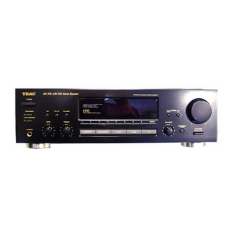
AM/FM Stereo Receiver
CONTENTS
1 SPECIFICATIONS
2 ADJUSTMENTS AND CHECKS
3 EXPLODED VIEWS AND PARTS LIST
4 PC BOARDS AND PARTS LIST
PC boards shown are viewed from parts side.
The parts with no reference number or no parts number in the
exploded views are not supplied.
As regards the resistors and capacitors, refer to the circuit diagrams
contained in this manual.
£
Parts marked with this sign are safety critical components. They
must be replaced with identical components - refer to the appropriate
parts list and ensure exact replacement.
NOTES
S-0091A
2
3
6
8
Advertisement

Subscribe to Our Youtube Channel
Related Manuals for Teac AG-370


Summary of Contents for Teac AG-370
- Page 1 SERVICE MANUAL A A G G - - 3 3 7 7 0 0 AM/FM Stereo Receiver CONTENTS 1 SPECIFICATIONS 2 ADJUSTMENTS AND CHECKS 3 EXPLODED VIEWS AND PARTS LIST 4 PC BOARDS AND PARTS LIST NOTES PC boards shown are viewed from parts side. The parts with no reference number or no parts number in the exploded views are not supplied.
-
Page 2: Specifications
1 SPECIFICATIONS Amplifier Section Voltage Conversion Output Power ..50 + 50 watts RMS (0.9 % THD, 1 kHz, 8 ohms) (General export models only) Total Harmonic Distortion....0.05 % (at 45 watts,1 kHz) Input Sensitivity/Impedance ....PHONO: 4 mV/22 kohms LINE: 270 mV/20 kohms Frequency Response.... -
Page 3: Adjustments And Checks
2 ADJUSTMENTS AND CHECKS 2-1 AMPLIFIER SECTION Bias Current Adjustment 1. Turn the unit on, and set the input selector switch to "CD". 2. Set 7VR1 and 7VR2 to the center position. 3. Connect the DC voltmeter as shown below after preheating for 10 minutes, and adjust 7VR1 (Lch) so that the voltage becomes 3.3 1.3mV. - Page 4 2-2 TUNER SECTION SETTING ADJUSTMENT ITEM ADJUST POINTS INPUT OUTPUT AG-370 FM 87.5 MHz 2L3 (3.5T) DC 1.0 0.05V FM 108.0 MHz Check DC 8.0 0.5V å 1. VT Adjust 2R19 (VT) 2J2 (GND) AM 530 kHz 2T2 (RED) DC 1.1 0.05V...
- Page 5 DC Voltmeter 2R19 TUNER PCB 2TC2 AM Signal Generator AM Loop Antenna AC Voltmeter 60cm FM Signal Generator AC Voltmeter Distortion Analyzer Stereo Signal Generator...
-
Page 6: Exploded Views And Parts List
3 EXPLODED VIEWS AND PARTS LIST... - Page 7 EXPLODED VIEW LIST £ £ £ £ £ £ £ £ INCLUDED ACCESSORIES...
- Page 8 4 PC BOARDS AND PARTS LIST MAIN PCB...
- Page 9 FRONT PCB TUNER PCB SP SEL PCB SP SEL PCB HEADPHONE PCB POW SEL PCB POWER PCB...
- Page 10 MAIN PCB ASSY CONTROL PCB ASSY £ £ £ £ £ £ TUNER PCB ASSY £ £ £ £ £ £ £ £ £ £ £ £...
- Page 11 SELECT PCB ASSY SELECT PCB ASSY HEADPHONE PCB ASSY £ POWER SELECT SW PCB ASSY £ POWER SOCKET PCB ASSY £ £...
-
Page 12: Schematic Diagram Main Pcb
AG-370 SCHEMATIC DIAGRAM MAIN PCB (1/2) 1XS2 1XP2 100U/16V TREBLE 4R17 4C19 -12V -12V 6VR2 100U/16V 6R13 6N1-1 6R17 6R23 4558D 4C15 6C11 4N1-1 4R13 4U7/50V 4558D 6C15 TREBLE 4R11 4R15 4C17 6VR2-1 180K 100K 4U7/50V 100KB 6C13 PHONO 4C11... - Page 13 AG-370 SCHEMATIC DIAGRAM MAIN PCB (2/2), HEADPHONE PCB, SP SEL PCB, POWER PCB, POW SEL PCB 1XP5 1XS5 7C25 7D11 7R41 4U7/50V 4148 7R75 330 7D12 7R25 7R29 4148 4148 7R76 7R67 7C29 REL1 103/50V 1XS8 1XP8 7V23 A/L- A/L-...
- Page 14 AG-370 SCHEMATIC DIAGRAM TUNER PCB LOOP 2C14 2R19 2VD3 2TC2 2C40 *2TC1 2R17 2D2 IN4148 V149B 3U3/50V 100K 100K 4.5T 2C44 2VD1 K161GR V104 2C12 2C25 2C11 C1815GR TA2149N 2C28 2C42 RFGND FMRF 4.5M 2R23 TC9257F RFIN RFVCC 3.5T 2R32...
- Page 15 AG-370 SCHEMATIC DIAGRAM FRONT PCB VFD 25114-1 470U/16 1N4148 DGND 8R21 1.8V AC 1 2 3 9 8 7 6 5 4 10 11 12 13 14 15 16 32 31 30 29 28 27 26 25 24 23 22 21 20 19 18 17 33 34 35 8R20 1.8V AC...
- Page 16 AG-370 SCHEMATIC DIAGRAM MAIN PCB (1/2) 1XS2 1XP2 100U/16V TREBLE 4R17 4C19 -12V -12V 6VR2 100U/16V 6R13 6N1-1 6R17 6R23 4558D 4C15 6C11 4N1-1 4R13 4U7/50V 4558D 6C15 TREBLE 4R11 4R15 4C17 6VR2-1 180K 100K 4U7/50V 100KB 6C13 PHONO 4C11...
- Page 17 AG-370 SCHEMATIC DIAGRAM MAIN PCB (2/2), HEADPHONE PCB, SP SEL PCB, POWER PCB, POW SEL PCB 1XP5 1XS5 7C25 7D11 7R41 4U7/50V 4148 7R75 330 7D12 7R25 7R29 4148 4148 7R76 7R67 7C29 REL1 103/50V 1XS8 1XP8 7V23 A/L- A/L-...
- Page 18 AG-370 SCHEMATIC DIAGRAM TUNER PCB LOOP 2C14 2R19 2VD3 2TC2 2C40 *2TC1 2R17 2D2 IN4148 V149B 3U3/50V 100K 100K 4.5T 2C44 2VD1 K161GR V104 2C12 2C25 2C11 C1815GR TA2149N 2C28 2C42 RFGND FMRF 4.5M 2R23 TC9257F RFIN RFVCC 3.5T 2R32...
- Page 19 AG-370 SCHEMATIC DIAGRAM FRONT PCB VFD 25114-1 470U/16 1N4148 DGND 8R21 1.8V AC 1 2 3 9 8 7 6 5 4 10 11 12 13 14 15 16 32 31 30 29 28 27 26 25 24 23 22 21 20 19 18 17 33 34 35 8R20 1.8V AC...
Need help?
Do you have a question about the AG-370 and is the answer not in the manual?
Questions and answers