JVC MX-G700R Service Manual

JVC MX-G700R Service Manual

Compact component system
Hide thumbs Also See for MX-G700R:

Advertisement

Quick Links

SERVICE MANUAL
COMPACT COMPONENT SYSTEM
STAN DBY/ ON
1
2
3
SUBW OOFER
SLEEP
LEVEL
4
5
6
AUX
SOUN D
M ODE
7
8
9
FM MODE
1 0
+1 0
DISPLAY
Ð SELECT +
M ODE
PTY/ EON
FM /A M
FADE
TAPE
TAPE A/B
M UTIN G
DISC
CD
SKIP
+
VOLUM E
VOLUM E
Ð
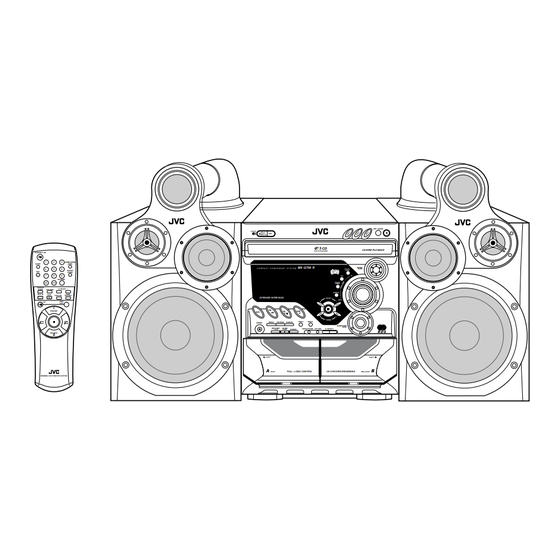
RM Ð SMXG 5 00 R R EM OTE CONT ROL
SP-MXGT700
Contents
Safety Precautions
Important for laser produbts
Preventing static electricity
Disassembly method
Wiring connection
Adjustment method
MX-G700R
STAND BY
ECO
STANDBY/ON
3
CD
MX -G700 R
CLOCK
/TIMER
DISPLAY
EXTEN DED SUPER BA SS
FM
CD
TAPE
AUX
/ AM
TUNING
TAPE A
TAPE B
REPEAT
PROGRAM
RANDOM
PHONES
SUBW OOFER
REC START
CD REC
/ STOP
START
DUBBING
DISPLAY M ODE PTY/ EON
Ð SE LECT +
FULL - L OGIC CONT ROL
CD SYN CHRO RECORDIN G
CA-MXG700R
1-2
Flow of functional operation
1-4
1-5
Maintenance of laser pickup
1-6
Replacement of laser pickup
1-19
Trouble shooting
1-20
Description of major ICs
COPYRIGHT
2002 VICTOR COMPANY OF JAPAN, LTD.
DISC CHANGE
CD-R/RW PLAYBACK
SOUND
M ODE
LEVEL
SP-MXGT700
until TOC read
MX-G700R
Area suffix
B ------------------------ U.K.
E ---- Continental Europe
EN ----- Northern Europe
EV ------- Eastern Europe
1-24
1-25
1-25
1-26
1-29~42
No.21103
May. 2002

Advertisement

Table of Contents
loading
Need help?

Need help?

Do you have a question about the MX-G700R and is the answer not in the manual?

Questions and answers

Subscribe to Our Youtube Channel

Summary of Contents for JVC MX-G700R

  • Page 1 MX-G700R SERVICE MANUAL COMPACT COMPONENT SYSTEM MX-G700R Area suffix B ------------------------ U.K. E ---- Continental Europe EN ----- Northern Europe EV ------- Eastern Europe DISC CHANGE STAND BY STANDBY/ON CD-R/RW PLAYBACK STAN DBY/ ON SUBW OOFER SLEEP LEVEL MX -G700 R...
  • Page 2 MX-G700R 1. This design of this product contains special hardware and many circuits and components specially for safety purposes. For continued protection, no changes should be made to the original design unless authorized in writing by the manufacturer. Replacement parts must be identical to those used in the original circuits. Services should be performed by qualified personnel only.
  • Page 3 MX-G700R (U.K only) 1. This design of this product contains special hardware and many circuits and components specially for safety purposes. For continued protection, no changes should be made to the original design unless authorized in writing by the manufacturer.
  • Page 4: Important For Laser Products

    MX-G700R Important for laser products 5.CAUTION : If safety switches malfunction, the laser is able 1.CLASS 1 LASER PRODUCT to function. 2.DANGER : Invisible laser radiation when open and inter 6.CAUTION : Use of controls, adjustments or performance of lock failed or defeated. Avoid direct exposure to beam.
  • Page 5: Preventing Static Electricity

    MX-G700R Preventing static electricity 1. Grounding to prevent damage by static electricity Electrostatic discharge (ESD), which occurs when static electricity stored in the body, fabric, etc. is discharged, can destroy the laser diode in the traverse unit (optical pickup). Take care to prevent this when performing repairs.
  • Page 6: Disassembly Method

    MX-G700R Metal cover Disassembly method Removing the metal cover (See Fig.1) Remove the three screws A attaching the metal cover on the back of the body. Remove the six screws B attaching the metal cover on the both sides of the body.
  • Page 7: Removing The Front Panel Assembly

    MX-G700R CW105 CD board CW107 Rear panel CD changer unit RCW6 Fig.6 Front panel assembly CD changer unit Main board (both sides) Fig.5 Rear panel Fig.7 FCW3 Removing the front panel assembly Main board JCW2 Front panel (See Fig.8 to 10)
  • Page 8: Removing The Fan Motor

    MX-G700R Removing the heat sink & amp. board Joint2 (Bottom side) (See Fig.8, 11 and 12) Prior to performing the following procedure, remove the metal cover and CD changer unit. Disconnect the card wire from the connector ACW1 and the harness from the connector ACW2, ACW5 and ACW6 on the amp.
  • Page 9 MX-G700R Removing the rear panel (See Fig.12) FCW3 Prior to performing the following procedure, remove JCW2 the metal cover, CD changer unit, heat sink & amp. JCW1 board and tuner board. Main board Fuse board HCW3 Remove the two screws O and three screws P attaching the rear panel.
  • Page 10 MX-G700R Front panel assembly (inner side) <Front panel assembly> CD switch board Prior to performing the following procedure, remove the metal cover, the CD changer unit and the front panel assembly. UCW1 Removing the CD switch board Front board (See Fig.1)
  • Page 11 MX-G700R CD changer uint (reverse side) <CD changer unit> Prior to performing the following procedure, remove the CD changer unit. CD board Removing the CD tray (See Fig.1 to 3) CW103 Turn the black loading pulley gear on the under side of the CD changer unit in the direction of the arrow and draw the CD tray toward the front until it stops.
  • Page 12 MX-G700R Removing the sensor board / the turn table motor assembly (See Fig.6 to 8) Prior to performing the following procedure, remove the CD tray. Remove the screw A attaching the sensor board and release the two tabs b attaching the sensor board on the under side of the CD tray.
  • Page 13 MX-G700R Removing the belt, the CD board and the switch board (See Fig.9 and 10) Belt Prior to performing the following procedure, remove the CD tray. Detach the belt from the pulley on the upper side of the CD changer unit (Do not stain the belt with grease).
  • Page 14 MX-G700R Removing the CD mechanism holder assembly (mechanism included) Motor connecter (See Fig.11 to 14) Disconnect the harness from connector on the CD mechanism board in the CD mechanism assembly on the under side of the CD changer unit. Disconnect the card wire from the pickup unit connector.
  • Page 15 MX-G700R CD mechanism section> Shutter Shaft Pickup unit emoving the CD mechanism holder from the CD hager unit. Refer to "Removing the CD mechanism holder ssembly" ) emoving the pickup unit ee Fig.1) 1. Removing the cut washer on the feed gear sleeve and pull out the feed gear.
  • Page 16 MX-G700R R/P Head <Cassette mechanism section> Removing the record/playback mechanism. Removing the R/P head. 1. Remove the screw A on the right side of the 2. Remove the screw B on the left side of the R/P head.(Fig.1, Fig.2) Remove the erase head.
  • Page 17: Removing The Motor

    MX-G700R Motor Mecha. terminal board Removing the motor. 1. Remove the two screws D fixing the motor. Be careful to grease's splash when the drive belt comes off.(Fig.5, Fig.6) 2. Unsolder the motor terminal.(Fig.5) Removing the mechanism board. Unsolder the four parts a on the solenoid...
  • Page 18 MX-G700R < Speaker section > It is exchange in a unit. Please do not decompose. Removing the net assembly (See Fig. 1) Remove the four bosses attaching the net assembly and remove the net assembly. Net assembly Boss Boss Fig.1...
  • Page 19: Wiring Connection

    MX-G700R Wiring connection Color codes are shown below. Brown Orange Yellow Green Blue Violet AH39-00045A Gray White Black 1-19...
  • Page 20: Adjustment Method

    MX-G700R Adjustment method 1. Tuner * Adjustment Location of Tuner PCB LW OSC LW RF AM(MW) RF AM(MW) OSC Adjustment Adjustment ITEAM Adjustment Adjustment Received FREQ. 594 KHz 144~288 KHz 150 KHz 522~1629 KHz Adjustment point Maximum Maximum 2~7.0V 1~7.0V Output Output(Fig.1)
  • Page 21 MX-G700R FM THD Adjustment SSG FREQ. 98 MHz Adjustment Output Antenna point FM DETECTOR COIL Terminal (FM DET) Oscilloscope FM S.S.G Input 60 dB Output Speaker Minumum Distortion (0.4% below) Terminal Input output (Fig.2) Distortion Meter Fig.2 IF CENTER and THD Adjustment FM Search Level Adjustment SSG FREQ.
  • Page 22 MX-G700R 2. Cassette Deck To adjust tape speed Notes Cassette Deck Frequency Counter 1) Measuring tape: i) VT-712/MTT-111(or equivalent) (Tapes recorded with 3kHz) SPK OUT ii) AC-225/MTT-5512(or equivalent) output Fig.1 2) Connect the cassette deck to the frequency counter as in fig.1.
  • Page 23 MX-G700R 2. Adjust Deck 2 Play Level/REC BIAS Pre-Setup Step Item Pre-Setup To Adjust Standard Remark Condition After putting VT-703 AZIMUTH SPK OUT Turn the control Max output After into Deck 2 (VTVM is screw to as and same phase...
  • Page 24: Flow Of Functional Operation Until Toc Read

    MX-G700R Flow of functional operation until TOC read Check Point Play Key Power ON RESET a CD LSI Confirm that the voltage at the pin17 of KB9226(IC101) is "L" "H". Confirm that the voltage at the pin33 LIMIT SW ON of KB9226(IC101) is "H"...
  • Page 25: Maintenance Of Laser Pickup

    MX-G700R Maintenance of laser pickup (1) Cleaning the pick up lens (2) Life of the laser diode Before you replace the pick up, please try to When the life of the laser diode has expired, clean the lens with a alcohol soaked cotton the following symptoms will appear.
  • Page 26: Troubleshooting

    MX-G700R Troubleshooting 1. Amplifier Power malfunction No output 1-26...
  • Page 27 MX-G700R 2.Tuner malfunction (FM/AM) 3.Tape HA12235F 3,4,27,28 HA12235F JIC1(HA12235F) PIN5,26 JC63L,JC63R,JR65L,JR65R 1-27...
  • Page 28 MX-G700R 4.CD 1-28...
  • Page 29: Description Of Major Ics

    MX-G700R Description of major ICs KA3082 (IC401, IC402) : DC motor driver 1.Pin layout 2.Pin function Pin No. Symbol Function DRIVER OUT Ground Output 1 Phase compensation PRE DRIVER Motor speed control VCTL Input 1 VIN1 VIN2 Input 2 LOGIC SWITCH...
  • Page 30 MX-G700R 5L9290 (IC201) : Digital signal processor for CDP 1. Pin layout VSSA_PLL BCKO VCO1LF LRCKO VSSD_PLL SADTO VDDD_PLL DATX VDDD1_5V C2PO S5L9290X JITB DSP+DAC XOUT SBCK 48-LQFP-0707 VSSD1_5V VDDD3-5V EFMI VSSD2-3V LOCK VDDD2-3V SMEF MUTE SMON SQDT 2. Block diagram...
  • Page 31 MX-G700R 3. Pin function Symbol Function VSSA_PLL Analog Ground for DPLL VCO1LF Pump out for VCO1 VSSD_PLL Digital Ground Separated Bulk Bias for DPLL VDDD_PLL Digital Power Separated Bulk Bias for DPLL (3V Power) VDDD1-5V Digital Power (5V Power, I/O PAD) X'tal oscillator input (16.9344MHz)
  • Page 32 MX-G700R KB9226 (IC101) : RF amp. & servo signal processor 1. Pin layout PDAC PDBD LOCK WDCK S1L9226X CLVI RESET DCCI DCCO MDATA VREF ISTAT 2. Block diagram Center Tracking Error RF & Focus RF AGC & EQ Voltage (RW)
  • Page 33 MX-G700R 3. Pin function Pin No. Symbol Function RF summing amp. inverting input RF summing amp. output RFO DC eliminating input(use by MIRROR, FOK ,AGC & EQ terminal) RF equalizer output EFMI EFM slice input. (input impedance 47K) Main power supply...
  • Page 34 MX-G700R LC72131(IC02) : PLL frequency synthesizer for electron alignment 1. Pin layout 2. Block diagram XOUT Phase Reference Detector Driver AOUT Charge Pump Swallow Counter FMIN 1/16,1/17 4bits Unlock AMIN Detector IFIN 12bits Programmable Divider Universal Data Shift Register & Latch...
  • Page 35 MX-G700R 3.Pin function (2/2) Symbol Pin No. Type Functions Circut confguration Used as the synchronization clock when serial data is input Clock to the LC72131 (DI ), or when serial data is output (DO). Inputs serial data sent from the controller to the LC72131M.
  • Page 36 MX-G700R LC86P6548 (UIC1) : Microcontroller 1.Pin layout S48/PG0 S19/PC3 S18/PC2 S49/PG1 S17/PC1 S50/PG2 S51/PG3 S16/PC0 VDD3 S15/T15 S14/T14 S13/T13 S12/T12 VSS2 S11/T11 VDD2 S10/T10 S9/T9 S8/T8 S7/T7 P10/SO0 S6/T6 S5/T5 P11/SI0/SB0 S4/T4 P12/SCK0 S3/T3 P13/SO1 P14/SI1/SB1 S2/T2 S1/T1 P15/SCK1 2.Block diagram...
  • Page 37 MX-G700R 3. Pin function Pin No. Symbol Function P16/BUZ Buzzer output P17/PWM0 Timer 1 output (PWM0 output) 8bit input/output port Input/output in bit unit 15V withstand at N-channel open drain output P70/INT0 INT0 input /HOLD release/N-channel Tr. ouptput forwatchdog timer...
  • Page 38 MX-G700R HA12235 (JIC1) : Audio signal processor 1. Block diagram REC OUT(L) REC OUT(R) ALC(L) ALC(R) REC IN(L) REC IN(R) PB OUT(L) PB OUT(R) TAI(L) TAI(R) EQOUT(L) EQOUT(R) PB-EQ(L) PB-EQ(R) PB-NF2(L) PB-NF2(R) 2. Pin function Pin No. Symbol Function Pin No.
  • Page 39 MX-G700R M66010 (UIC2) : I/O control 1.Pin layout 2.Block diagram Shift register 1 SERIAL DATA OUTPUT D24 D23 D22 D3 D2 D1 CLOCK INPUT SET INPUT CHIP SELECT Q24 Q23 Q22 Q3 Q2 Q1 PARALLEL INPUT Parallel output latch DATA I/O...
  • Page 40 MX-G700R TDA7442D (FIC1) : Audio processor 1.Pin layout R_IN3 R_IN4 R_IN2 LOUT R_IN1 ROUT L_IN1 AGND L_IN2 L_IN3 CREF L_IN4 MUXOUTL IN(L) DIG-GND MUXOUT(R) TREBLE(R) IN(R) TREBLE(L) BIN(R) BOUT(R) BIN(L) BOUT(L) 2.Block diagram 5.6K 5.6nF 100nF 100nF 100nF 2.2 F...
  • Page 41 MX-G700R L4959 (RIC1) : Voltage regulator 1.Pin layout OUT 12V(a) OUT 8.6V EN 8.6V EN 12V(a) EN 12V(b) N.C. OUT 5.6V OUT 12V(b) TAB CONNECTED TO PIN 6 D97AU716A 2.Block diagram 2/10 5.6V, 250mA OUT 5.6V REGULATOR 8.6V, 600mA OUT 8.6V...
  • Page 42 MX-G700R KA9258D (IC301) : 4-ch Motor driver 1.Block diagram 28 27 26 25 24 23 22 21 20 19 18 17 16 15 REGULATOR T • S • D MUTE 10 11 12 13 14 LA1837 (IC01) : FM IF/DET AM RF/IF/DET 1.Block diagram...
  • Page 43 MX-G700R < M E M O > 1-43...
  • Page 44 MX-G700R VICTOR COMPANY OF JAPAN, LIMITED AUDIO & COMMUNICATION BUSINESS DIVISION PERSONAL & MOBILE NETWORK BUSINESS UNIT. 10-1,1chome,Ohwatari-machi,Maebashi-city,371-8543,Japan (No.21103) 200205...

This manual is also suitable for:

Sp-mxgt700Ca-mxg700r

Table of Contents