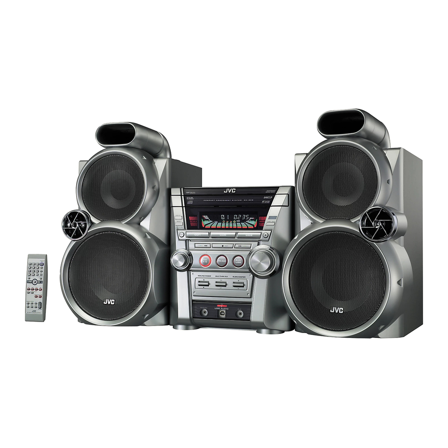
JVC MX-GC5 Service Manual
Compact component system
Hide thumbs
Also See for MX-GC5:
- Service manual (68 pages) ,
- Instructions manual (30 pages) ,
- Instructions manual (30 pages)
Table of Contents
Advertisement
Quick Links
SERVICE MANUAL
COMPACT COMPONENT SYSTEM
SP-MXGC5
Contents
Safety precautions ---------------------------- 1- 2
Preventing static electricity ----------------- 1- 3
Important for laser products ---------------- 1- 4
Disassembly method ------------------------ 1- 5
Adjustment method -------------------------- 1- 18
All manuals and user guides at all-guides.com
MX-GC5
CA-MXGC5
COPYRIGHT © 2005 Victor Company of Japan,Limited
SP-MXGC5
Flow of functional
operation until TOC read -------------- 1- 20
Maintenance of laser pickup -------------- 1- 21
Replacement of laser pickup -------------- 1- 21
Description of major ICs ------------------- 1- 22
MX-GC5
Area Suffix
J ........................ U.S.A.
C ........................ Canada
Advertisement
Table of Contents

Related Manuals for JVC MX-GC5


Summary of Contents for JVC MX-GC5
- Page 1 All manuals and user guides at all-guides.com MX-GC5 SERVICE MANUAL COMPACT COMPONENT SYSTEM MX-GC5 SP-MXGC5 CA-MXGC5 SP-MXGC5 Area Suffix J ......U.S.A. C ......Canada Contents Safety precautions ---------------------------- 1- 2 Flow of functional Preventing static electricity ----------------- 1- 3...
- Page 2 All manuals and user guides at all-guides.com Safety Precautions 1. This design of this product contains special hardware and many circuits and components specially for safety purposes. For continued protection, no changes should be made to the original design unless authorized in writing by the manufacturer.
-
Page 3: Preventing Static Electricity
All manuals and user guides at all-guides.com Preventing static electricity 1. Grounding to prevent damage by static electricity Electrostatic discharge (ESD), which occurs when static electricity stored in the body, fabric, etc. is discharged, can destroy the laser diode in the traverse unit (optical pickup). Take care to prevent this when performing repairs. -
Page 4: Important For Laser Products
All manuals and user guides at all-guides.com Important for laser products 1. CLASS 1 LASER PRODUCT 5. CAUTION : If safety switches malfunction, the laser is able to function. 2. DANGER : Invisible laser radiation when open and inter lock failed or defeated. Avoid direct exposure to beam. 6. -
Page 5: Disassembly Method
All manuals and user guides at all-guides.com Disassembly method Commence disassembly of the set by removing the main units and then proceed to the components and assemblies inside the units. Replacement of the fuses and the power IC Top cover CD changer unit Front panel assembly CD changer unit... - Page 6 All manuals and user guides at all-guides.com <Disassembly of the main blocks of the set> Replacement of the fuses and the power IC Replacing the fuses (See Fig.1) Replacing the heat sink cover (See Fig.3) Prior to performing the following procedure, remove 1.
-
Page 7: Removing The Top Cover
All manuals and user guides at all-guides.com Removing the top cover (See Fig.4 and 5) 1. Remove six screws C that retain the top cover from the panel rear of the body. 2. Remove six screws D that retain the top cover from the two sides of the body. - Page 8 All manuals and user guides at all-guides.com Removing the CD changer unit (See Fig.6 to 9) Prior to performing the following procedures, remove the top cover. [Caution] Although the CD mechanism unit can be removed without removing the CD tray panel, it is still recommended to remove it in order to prevent damage.
- Page 9 All manuals and user guides at all-guides.com Removing the front panel assembly (See Fig.10 to 11) Prior to performing the following procedures, remove the top cover. Also remove the CD changer unit. 1. Disconnect the parallel wire and the cord wire from the connectors CN201, CN401 on the main PCB.
-
Page 10: Removing The Main Pcb
All manuals and user guides at all-guides.com <Disassembly of units and assembly inside this set> Removing the MAIN PCB (See Fig.12 to 13) CD PCB Prior to performing the following procedures, remove the top cover. Also remove the CD changer unit. 1. - Page 11 All manuals and user guides at all-guides.com Removing the CD changer mechanism CD changer assembly (See Fig.14 to 15) unit Prior to performing the following procedures, remove the top cover. Also remove the CD changer unit. 1. Turn the CD changer mechanism cover base and remove the screws d connecting the unit to the CD changer mechanism assembly.
- Page 12 All manuals and user guides at all-guides.com Removing the CD pickup (See Fig.16) CD pickup Prior to performing the following procedures, remove the top cover. Also remove the CD changer unit. Also remove the CD changer mechanism. 1. Widen the section f. 2.
-
Page 13: Removing The Display Pcb
All manuals and user guides at all-guides.com Removing the USB,AUX,earphone PCB (See Fig.19) Prior to performing the following procedures, remove Front panel the top cover. assembly Also remove the CD changer unit. Also remove the front panel assembly. R( 17PCS) Remove six screws Z retaining the USB,AUX, earphone PCB. - Page 14 All manuals and user guides at all-guides.com Removing sound mode and volume , pre- set and CD function switch PCB (See Fig.20 to 23) Front panel assembly Prior to performing the following procedures, remove the top cover. Also remove the CD changer unit. Also remove the front panel assembly.
- Page 15 All manuals and user guides at all-guides.com Removing the bridge diode (See D214, D215 and Fig.28) Prior to performing the following procedures, remove the top cover and both sides board. 1. Remove two screws W that connect the heat sink. 2.
-
Page 16: Flow Of Functional Operation Until Toc Read
All manuals and user guides at all-guides.com Flow of functional operation until TOC read Check Point Slider turns REST Confirm that the voltage at the pin5 Play Key Power ON SW ON. of CN702 is "H"\"L"\"H". Automatic tuning of TE offset Check that the voltage at the Laser ON pin10 of IC701 is + 0V? -
Page 17: Maintenance Of Laser Pickup
All manuals and user guides at all-guides.com Maintenance of laser pickup Replacement of laser pickup (1) Cleaning the pick up lens Turn off the power switch and,disconnect the Before you replace the pick up, please try to clean power cord from the AC OUTLET. the lens with a alcohol soaked cotton swab. -
Page 18: Test Circuit
All manuals and user guides at all-guides.com Description of major ICs STK412-430 (IC201) : Dual low noise operational 1. Equivalent Block Diagram TR41 Comparator TR12 TR11 TR16 TR19 TR14 TR13 TR18 TR10 TR20 TR15 TR17 Comparator TR51 11 10 2. Test Circuit 1 2 3 4 5 6 7 8 9 10 11 12 13 14 15 16 17 18... - Page 19 All manuals and user guides at all-guides.com CD DRIVE ICS BA5927FM(IC702)
- Page 20 All manuals and user guides at all-guides.com BA4558F (IC503) : Dual low noise operational amp. 1. Terminal layout 1. Pin descriptions OUT1 - IN1 OUT2 +IN1 - IN2 +IN2 1chip AM/FM, MPX tuner system 1. Block diagram GND2 VCC2 MUTE PHASE PILOT DECODER...
- Page 21 All manuals and user guides at all-guides.com RHYTHM AX (IC502) JCV8011 : Block diagram...
-
Page 22: Application Diagram
All manuals and user guides at all-guides.com RF AMP & SERVO SIGNAL PROCESSOR (IC701): S1L9226X 1. Application diagram 10 F 120k 100k 47 F 39k 104 150k 120k 100k Pick-up 100k PDAC PDBD to DSP LOCK From DSP From DSP WDCK SMDP S1L9226X... - Page 23 All manuals and user guides at all-guides.com 2. Block diagram Center Tracking Error RF & Focus RF AGC & EQ Voltage (RW) Error (CD-RW) Control I/V AMP I/V AMP EFMI Focus OK Detect Defect Detect Mirror APC. Laser DCCI Control & LPFT DCC0 TEIO...
- Page 24 All manuals and user guides at all-guides.com 3. Pin description Table 1. Pin Description Pin No. Symbol Description RF summing amp. inverting input RF summing amp. output RFO DC eliminating input(use by MIRROR, FOK ,AGC & EQ terminal) RF equalizer output EFMI EFM slice input.
- Page 25 All manuals and user guides at all-guides.com Table 1. Pin Description (Continued) Pin No. Symbol Description Main ground TZC/ Tracking zero crossing input & Check the position of pick-up wherther inside or SSTOP TEIO Tracking error output & Tracking servo input LPFT Tracking error integration input (to automatic control) ATSC...
-
Page 26: Electrical Characteristics
All manuals and user guides at all-guides.com 5. Electrical characteristics Table 2. Electrical Characteristics Spec Characteristics Symbols Test Block Unit Min. Typ. Max. Supply current 2.7V ICCTY RF AMP offset voltage Vrfo RF AMP -100 RF AMP offset voltage 2 Vrfo2 -300 -200... - Page 27 All manuals and user guides at all-guides.com 32X16 VFD DRIVER & CONTROLLER preliminary DATASHEET (IC402) 1. Sample application circuit Panel : 11Grid & 29Seg The value of control register Display Mode Control Register(dsp) : 111 ( default) Display Sub Time Control Register(tsub) : 101 ( -5 ) +5V VDD LED6 LED5...
- Page 28 All manuals and user guides at all-guides.com 2. Block diagram S33/G16 S39/G10 S1 to S32 G9 to G1 SEG/GRID GRID SEG DRIVER DRIVER DRIVER 40-bi t seg l atc h 16-bi t gr id atch 40X16 16X16 SEG RA M GRID RA M Ser ial I/F LE D6...
- Page 29 All manuals and user guides at all-guides.com 3. Pin description Pin No. Name Function IN/OUT 1 to 3 S3 to S1 Segment driver output pins (segment only). This is P-ch open-drain output with pull-down resistor 5 to 10 LED6 to 6 LED driver output ports.
- Page 30 All manuals and user guides at all-guides.com CD-MP3 Decoder Specification (IC804) 1. PKG Type : 100 TQFP PKG RFCK MNT0 MNT1 MNT2 MNT3 MNT4 MNT5 INT_DVSS0 XOUT INT_DVSS0 LDQM INTVDD2 S5L9279X INTVSS2 /DRW RESETB CD-MP3 1 Chip Data Processor /CAS EFMI /RAS ISTAT...
- Page 31 All manuals and user guides at all-guides.com 2. CD-MP3 1 Chip Block Diagram DATX MEMORY I/ F Digital LCHOUT Output RCHOUT MEMORY INTERNAL INTERNAL CONTROL BLOCK MEMORY MEMORY ADPCM BANK1 BANK 2 SDAT ENC/ DEC Subc ode SBCK Output LKFS 1 Bit DATA PCM DATA...
- Page 32 All manuals and user guides at all-guides.com SYSTEM IC (IC301) S3P825A P0.7/SEG23 P7.2/SEG6 P1.0/SEG24 P7.1/SEG5 P1.1/SEG25 P7.0/SEG4 P1.2/SEG26 P6.7/SEG3/COM7 P1.3/SEG27 P6.6/SEG2/COM6 P1.4/SEG28 P6.5/SEG1/COM5 P1.5/SEG29 P6.4/SEG0/COM4 P1.6/SEG30 P6.3/COM3 P1.7/SEG31 P6.2/COM2 P2.0 P6.1/COM1 P2.1 P6.0/COM0 S3P825A (80-QFP-1420C) P5.6 TEST P5.5/TXD P5.4/RXD P5.3/BUZ RESET P5.2/SO P2.2/T2CLK...
-
Page 33: Pin Descriptions
All manuals and user guides at all-guides.com 2. PIN DESCRIPTIONS Table 1-1. S3C825A Pin Descriptions Circuit Share Type Description Type Numbers Pins Names P0.0–P0.7 4-bit-programmable I/O port. H-32 72–79 SEG16 Input or push-pull, open-drain output and (74-80, 1) – software assignable pull-ups. SEG23 P1.0–1.7 4-bit-programmable I/O port. - Page 34 All manuals and user guides at all-guides.com Table 1-1. S3C825A Pin Descriptions (Continued) Circuit Share Names Type Description Type (note) Pins Numbers – Power input pins for core block – 10, 11 (12, 13) – – Main oscillator pins – 12, 13 (14, 15) –...
- Page 35 All manuals and user guides at all-guides.com Printed in Japan...
-
Page 36: Parts List
All manuals and user guides at all-guides.com PARTS LIST [ MX-GC5 ] * All printed circuit boards and its assemblies are not available as service parts. Area suffix J ----------------------------- U.S.A. C -------------------------- Canada - Contents - 3- 2 Exploded view of general assembly and parts list (Block No.M1) 3- 5 CD changer mechanism assembly and parts list (Block No.MA) -
Page 37: Exploded View Of General Assembly And Parts List
All manuals and user guides at all-guides.com Exploded view of general assembly and parts list Block No. Main board F902... - Page 38 All manuals and user guides at all-guides.com F902 Power trans. board Amp. board F901...
-
Page 39: General Assembly
All manuals and user guides at all-guides.com General Assembly Block No. [M][1][M][M] Symbol No. Part No. Part Name Description Local BI251030093100V 3CD MECHANISM BIZ25094901VV TUNER PACK BIBT000410S3 SCREW 6XL10(x11) BIBT000418 SCREW 6XL18(x47) BIBT000608 SCREW 3XL12(x14) BIBT000654 SCREW 3XL16(x2) BI1081740101X1 VFD BOX L BI1081750101X1 VFD BOX R... - Page 40 All manuals and user guides at all-guides.com CD loading mechanism assembly and parts list Block No. CMS-FR3BN 9 10 The parts without symbol number are not service.
-
Page 41: Cd Loading Mechanism
All manuals and user guides at all-guides.com CD loading mechanism Block No. [M][A][M][M] Symbol No. Part No. Part Name Description Local BIAJ7200601J BASE-MAIN BIAJ6100601P BRKT-CHUCK BI3302000158 MAGNET-FERRITE BIAJ7200601L TABLE-CHUCK BIAJ6300601A SHEET-CHUCK (x3) BIAJ7300601B BELT-LOAD BIAJ6600601N GEAR-SYNCRO BIAJ6600601L GEAR-CONVERT BIAJ6600601M GEAR-TRAY BIAJ6600601R GEAR-CAM... -
Page 42: Electrical Parts List
All manuals and user guides at all-guides.com Electrical parts list Main board Symbol No. Part No. Part Name Description Local Block No. [0][1] BI31SS133M000V D508 1SS133 FR DIODE Symbol No. Part No. Part Name Description Local BI3UZ9.1BSCM00 D571 UZ9.1BSC Z DIODE BI31SS133M000V... - Page 43 All manuals and user guides at all-guides.com Symbol No. Part No. Part Name Description Local Symbol No. Part No. Part Name Description Local C516 BICM224101KP015 M CAPACITOR 0.22uF C729 BICC102500KA042 C CAPACITOR 1000pF 50V C517 BICE106500MP015 E CAPACITOR 10uF C730 BICC222500KA042...
- Page 44 All manuals and user guides at all-guides.com Symbol No. Part No. Part Name Description Local Symbol No. Part No. Part Name Description Local R326 BIRC2230085M000 C RESISTOR 22KΩ R434 BIRC4730105A005 C RESISTOR 47KΩ R327 BIRC1020105A005 C RESISTOR 1KΩ R435 BIRC4740105A005 C RESISTOR...
-
Page 45: Front Board
All manuals and user guides at all-guides.com Symbol No. Part No. Part Name Description Local Symbol No. Part No. Part Name Description Local R708 BIRC4700105A005 C RESISTOR 47KΩ CN501 BI12S120010 FFC CONNECTOR R709 BIRC4720105A005 C RESISTOR 4.7KΩ CN601 BI12S240004V FFC CONNECTOR R710... - Page 46 All manuals and user guides at all-guides.com Symbol No. Part No. Part Name Description Local Symbol No. Part No. Part Name Description Local C407 CC104500KA042 C CAPACITOR 0.1uF 50V R430 RC6220105A005 C RESISTOR 6.2KΩ C408 CC104500KA042 C CAPACITOR 0.1uF 50V R433 BIRC1010085M000...
-
Page 47: Amp Board
All manuals and user guides at all-guides.com Symbol No. Part No. Part Name Description Local Symbol No. Part No. Part Name Description Local S425 BI8SKRGAED0P015 TACT SWITCH SKRGAED010 BI3UZ6.2BSBM000 D210 UZ6.2BSB Z DIODE S426 BI8SKRGAED0P015 TACT SWITCH SKRGAED010 BI3UZ5.6BSBM000 S427 BI8SKRGAED0P015... - Page 48 All manuals and user guides at all-guides.com Symbol No. Part No. Part Name Description Local Symbol No. Part No. Part Name Description Local C215 BICC103500KA042 C CAPACITOR 0.01uF 50V R251 BIRC4720105A005 C RESISTOR 4.7KΩ C216 BICE477100MP015 E CAPACITOR 470uF R261 BIRC6830105A005...
-
Page 49: Power Trans. Board
All manuals and user guides at all-guides.com Symbol No. Part No. Part Name Description Local Symbol No. Part No. Part Name Description Local R2087 BIRC1020105A005 C RESISTOR 1KΩ 1/10W R2088 BIRC1020105A005 C RESISTOR 1KΩ 1/10W BI31SS133M000V D901 1SS133 FR DIODE R2091 BIRC3310105A005... - Page 50 All manuals and user guides at all-guides.com <MEMO> 3-15...
-
Page 51: Packing Materials And Accessories Parts List
All manuals and user guides at all-guides.com Packing materials and accessories parts list Block No. No additional / supplemental order of WARRANTY CARDs are available. A4 A5 A1 A2 3-16... -
Page 52: Packing And Accessories
All manuals and user guides at all-guides.com Packing and Accessories Block No. [M][3][M][M] Symbol No. Part No. Part Name Description Local BI440001560000W INST BOOK ENG FRE BI440001506000W INST BOOK ------------ WARRANTY CARD BT520062 ------------ WARRANTY CARD BT510341 BI400023260002W SAFTEY CARD ------------ BATTERY (x2) -
Page 53: Block Diagram
All manuals and user guides at all-guides.com BLOCK DIAGRAM... - Page 54 All manuals and user guides at all-guides.com WIRE ASS'Y BLOCK DIAGRAN...
-
Page 55: Main Schematic Diagram
All manuals and user guides at all-guides.com MAIN SCHEMATIC DIAGRAM(1/3) - Page 56 All manuals and user guides at all-guides.com MAIN SCHEMATIC DIAGRAM(2/3)
- Page 57 All manuals and user guides at all-guides.com MAIN SCHEMATIC DIAGRAM(3/3)
-
Page 58: Amp Schematic Diagram
All manuals and user guides at all-guides.com AMP SCHEMATIC DIAGRAM... - Page 59 All manuals and user guides at all-guides.com Power SCHEMATIC DIAGRAM...
-
Page 60: Front Schematic Diagram
All manuals and user guides at all-guides.com FRONT SCHEMATIC DIAGRAM... -
Page 61: Usb Schematic Diagram
All manuals and user guides at all-guides.com USB SCHEMATIC DIAGRAM... - Page 62 All manuals and user guides at all-guides.com AMP PCB BOTTOM...
- Page 63 All manuals and user guides at all-guides.com AMP PCB TOP...
-
Page 64: Front Pcb Bottom
All manuals and user guides at all-guides.com FRONT PCB BOTTOM... -
Page 65: Front Pcb Top
All manuals and user guides at all-guides.com FRONT PCB TOP... -
Page 66: Main Pcb Bottom
All manuals and user guides at all-guides.com MAIN PCB BOTTOM... -
Page 67: Main Pcb Top
All manuals and user guides at all-guides.com MAIN PCB TOP... - Page 68 All manuals and user guides at all-guides.com PT PCB TOP...
Need help?
Do you have a question about the MX-GC5 and is the answer not in the manual?
Questions and answers