Table of Contents
Advertisement
Quick Links
Advertisement
Table of Contents

Related Manuals for Asus AAEON GENE-ADN6


Summary of Contents for Asus AAEON GENE-ADN6
- Page 1 GENE-ADN6 3.5” Subcompact Board User’s Manual 2 Last Updated: June 28, 2024...
- Page 2 Copyright Notice This document is copyrighted, 2024. All rights are reserved. The original manufacturer reserves the right to make improvements to the products described in this manual at any time without notice. No part of this manual may be reproduced, copied, translated, or transmitted in any form or by any means without the prior written permission of the original manufacturer.
- Page 3 Acknowledgements All other products’ name or trademarks are properties of their respective owners. Microsoft Windows is a registered trademark of Microsoft Corp. ⚫ Intel Atom® is a registered trademark of Intel Corporation ⚫ Intel® Core™ is a trademark of Intel Corporation ⚫...
- Page 4 Packing List Before setting up your product, please make sure the following items have been shipped: Item Quantity GENE-ADN6 If any of these items are missing or damaged, please contact your distributor or sales representative immediately. Preface...
- Page 5 About this Document This User’s Manual contains all the essential information, such as detailed descriptions and explanations on the product’s hardware and software features (if any), its specifications, dimensions, jumper/connector settings/definitions, and driver installation instructions (if any), to facilitate users in setting up their product. Users may refer to the product page at AAEON.com for the latest version of this document.
- Page 6 Safety Precautions Please read the following safety instructions carefully. It is advised that you keep this manual for future references All cautions and warnings on the device should be noted. Make sure the power source matches the power rating of the device. Position the power cord so that people cannot step on it.
- Page 7 If any of the following situations arises, please the contact our service personnel: Damaged power cord or plug Liquid intrusion to the device iii. Exposure to moisture Device is not working as expected or in a manner as described in this manual The device is dropped or damaged Any obvious signs of damage displayed on the device...
- Page 8 FCC Statement This device complies with Part 15 FCC Rules. Operation is subject to the following two conditions: (1) this device may not cause harmful interference, and (2) this device must accept any interference received including interference that may cause undesired operation.
- Page 9 China RoHS Requirements (CN) 产品中有毒有害物质或元素名称及含量 AAEON Main Board/ Daughter Board/ Backplane 有毒有害物质或元素 部件名称 铅 汞 镉 六价铬 多溴联苯 多溴二苯醚 (Pb) (Hg) (Cd) (Cr(VI)) (PBB) (PBDE) 印刷电路板 ○ ○ ○ ○ 及其电子组件 外部信号 ○ ○ ○ ○ 连接器及线材 O:表示该有毒有害物质在该部件所有均质材料中的含量均在 SJ/T 11363-2006 标准规定的限量要求以下。 X:表示该有毒有害物质至少在该部件的某一均质材料中的含量超出...
- Page 10 China RoHS Requirement (EN) Poisonous or Hazardous Substances or Elements in Products AAEON Main Board/ Daughter Board/ Backplane Poisonous or Hazardous Substances or Elements Hexavalent Polybrominated Polybrominated Component Lead Mercury Cadmium Chromium Biphenyls Diphenyl Ethers (Pb) (Hg) (Cd) (Cr(VI)) (PBB) (PBDE) PCB &...
-
Page 11: Table Of Contents
Table of Contents Chapter 1 - Product Specifications..................1 Specifications ......................2 Block Diagram ......................6 Chapter 2 – Hardware Information ..................7 Dimensions ....................... 8 Jumpers and Connectors ..................10 List of Jumpers ......................12 2.3.1 COM 2 Pin 9 Function Selection (JP1) ............13 2.3.2 COM 1 Pin 9 Function Selection (JP2) ............ - Page 12 2.4.13 LAN Port 1 LED Connector (CN22) ............24 2.4.14 LAN Port 3 LED Connector (CN23)............25 2.4.15 LAN Port 2 LED Connector (CN24) ............25 2.4.16 M.2 3052 B-Key (CN25) ................26 2.4.17 Full Size Mini Card Slot/mSATA (CN27) ........... 26 2.4.18 LVDS 1 Connector (CN28) ................
- Page 13 Chapter 3 - AMI BIOS Setup ....................54 System Test and Initialization ................55 AMI BIOS Setup ..................... 56 Setup Submenu: Main ..................57 Setup Submenu: Advanced ................. 58 3.4.1 CPU Configuration ..................59 3.4.2 PCH-FW Configuration ................60 3.4.3 Firmware Update Configuration ..............
- Page 14 3.5.4 PCH-IO Configuration ................85 Setup Submenu: Security ..................86 3.6.1 Secure Boot ....................87 3.6.2 Key Management ..................88 Setup Submenu: Boot ..................90 3.7.1 BBS Priorities ....................91 Setup Submenu: Save & Exit ................92 Chapter 4 – Driver Installation ..................... 93 Driver Download/Installation ................
-
Page 15: Chapter 1 - Product Specifications
Chapter 1 Chapter 1 - Product Specifications... -
Page 16: Specifications
Specifications System Form Factor 3.5" SubCompact Board Intel Atom® x7000E Series, Intel® Processor N-series, Intel® Core™ i3-N305 Processors: Intel® Core™ i3-N305 (8C/8T, up to 3.8 GHz, 15W) Intel Atom® x7425E (4C/4T, up to 3.4 GHz, 12W) Intel® Processor N97 (4C/4T, up to 3.6 GHz, 12W) Intel®... - Page 17 Power Power Consumption Intel® Core™ i3-N305, DDR5 16GB x 1, 3.4A @+12V (Typical) Intel® Core™ i3-N305, DDR5 16GB x 1, 5.24A @+12V (Max) Display Controller Intel® UHD Graphics LVDS/eDP LVDS x 1, Dual Channel 18/24-bit, up to 1920 x 1080 Display Interface HDMI 1.4 x 1, up to 3840 x 2160 @30Hz VGA x 1, up to 1920 x 1080...
- Page 18 Internal I/O USB 2.0 x 4 Serial Port COM 1, COM 2 (RS-232/422/485, supports 5V/12V/RI) COM 3, COM 4 (RS-232) Video LVDS x 1 Inverter x 1 (12V/2A) SATA SATA 6Gb/s x 1 +5V SATA Power Connector x 1 Audio Audio Header x 1 (Optional) DIO/GPIO GPIO 8-bit...
- Page 19 Environmental Operating Humidity 0% ~ 90% relative humidity, non-condensing MTBF (Hours) 337,963 CE/FCC Class A Chapter 1 – Product Specifications...
-
Page 20: Block Diagram
Block Diagram Chapter 1 – Product Specifications... -
Page 21: Chapter 2 - Hardware Information
Chapter 2 Chapter 2 – Hardware Information... -
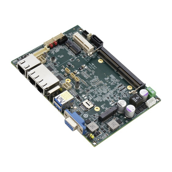
Page 22: Dimensions
Dimensions Component Side Chapter 2 – Hardware Information... - Page 23 Component Side 3D View Chapter 2 – Hardware Information...
-
Page 24: Jumpers And Connectors
Jumpers and Connectors Top View Front I/O View Chapter 2 – Hardware Information... - Page 25 Bottom View Chapter 2 – Hardware Information...
-
Page 26: List Of Jumpers
List of Jumpers Please refer to the table below for all of the board’s jumpers that you can configure for your application Label Function COM 2 Pin 9 Function Selection COM 1 Pin 9 Function Selection Auto Power Button Enable/Disable Selection LVDS 1 Operating Voltage Selection LVDS 1 Backlight Inverter Voltage Selection Clear CMOS Jumper... -
Page 27: Com 2 Pin 9 Function Selection (Jp1)
2.3.1 COM 2 Pin 9 Function Selection (JP1) 2.3.2 COM 1 Pin 9 Function Selection (JP2) 2.3.3 Auto Power Button Enable/Disable Selection (JP3) Chapter 2 – Hardware Information... -
Page 28: Lvds 1 Operating Voltage Selection (Jp4)
2.3.4 LVDS 1 Operating Voltage Selection (JP4) 2.3.5 LVDS 1 Backlight Inverter Voltage Selection (JP4) 2.3.6 Clear CMOS Jumper (JP5) Chapter 2 – Hardware Information... -
Page 29: List Of Connectors
List of Connectors Please refer to the table below for all of the board’s connectors that you can configure for your application Label Function +5V Output for SATA HDD Front Panel Port 80 Debug Port Connector SPI Flash Programming Port SATA Port External +12V Input (Optional) External Power Input... - Page 30 Label Function CN44 COM Port 1 CN45 COM Port 2 CN46 COM Port 3 CN47 COM Port 4 CN48 USB 2.0 Port 3 CN49 USB 2.0 Port 4 CN50 USB 2.0 Port 5 CN53 USB 2.0 Port 6 Chapter 2 – Hardware Information...
-
Page 31: Output For Sata Hdd (Cn1)
2.4.1 +5V Output for SATA HDD (CN1) Pin Name Signal Type Signal Level +V5S Note: The driving current of +V5S supports up to 2A. 2.4.2 Front Panel (CN2) Pin Name Signal Type Signal Level EXT_PWRBTN# SATA_LED- SATA_LED+ BUZZER- BUZZER+ Chapter 2 – Hardware Information... -
Page 32: Port 80 Debug Port Connector (Cn3)
Pin Name Signal Type Signal Level PWR_LED+ HWRST# 2.4.3 Port 80 Debug Port Connector (CN3) Pin Name Signal Type Signal Level ESP_IO0 +1.8V ESP_IO1 +1.8V ESP_IO2 +1.8V ESP_IO3 +1.8V +V3P3S +3.3V ESPI_CS ESPI_RST +3.3V ESPI_CLK +1.8V +V3P3A +3.3V Chapter 2 – Hardware Information... -
Page 33: Spi Flash Programming Port (Cn4)
2.4.4 SPI Flash Programming Port (CN4) Pin Name Signal Type Signal Level SPI_MISO SPI_CLK +V3P3A_SPI +3.3V SPI_MOSI SPI_CS Chapter 2 – Hardware Information... -
Page 34: Sata Port (Cn5)
2.4.5 SATA Port (CN5) Pin Name Signal Type Signal Level SATA_TX+ DIFF SATA_TX- DIFF SATA_RX- DIFF SATA_RX+ DIFF 2.4.6 External +12V Input (Optional) (CN8) Pin Name Signal Type Signal Level Chapter 2 – Hardware Information... -
Page 35: External Power Input (Cn9)
Pin Name Signal Type Signal Level +12V +12V +12V +12V 2.4.7 External Power Input (CN9) +12V GND Pin Name Signal Type Signal Level +12V +12V 2.4.8 Audio I/O Port (CN11) Pin Name Signal Type Signal Level RIGHT_OUT MIC_R LEFT_OUT Chapter 2 – Hardware Information... -
Page 36: Ddr5 So-Dimm Channel (Cn12)
Pin Name Signal Type Signal Level MIC_L JD_LOUT JD_MIC GND_AUDIO GND_AUDIO JD_LIN LINE_R_IN +5V_AUDIO LINE_L_IN 2.4.9 DDR5 SO-DIMM Channel (CN12) Standard Specifications. 2.4.10 External +5VSB Input (CN13) Pin Name Signal Type Signal Level PS_ON# +5VSB +5V at 2A Chapter 2 – Hardware Information... -
Page 37: Gpio Port (Cn18)
2.4.11 GPIO Port (CN18) Pin Name Signal Type Signal Level GPIO_0 IN/OUT GPIO_1 IN/OUT GPIO_2 IN/OUT GPIO_3 IN/OUT GPIO_4 IN/OUT GPIO_5 IN/OUT GPIO_6 IN/OUT GPIO_7 IN/OUT +V5S Note: The driving current of +V5S supports up to 0.5A. Chapter 2 – Hardware Information... -
Page 38: 2230 E-Key (Cn21)
2.4.12 M.2 2230 E-Key (CN21) Note: Standard specifications. 2.4.13 LAN Port 1 LED Connector (CN22) Pin Name Signal Type Signal Level +V3P3A +3.3V LAN1_1000# LAN1_ACT# LAN1_2500# Chapter 2 – Hardware Information... -
Page 39: Lan Port 3 Led Connector (Cn23)
2.4.14 LAN Port 3 LED Connector (CN23) Pin Name Signal Type Signal Level +V3P3A +3.3V LAN3_1000# LAN3_ACT# LAN3_2500# 2.4.15 LAN Port 2 LED Connector (CN24) Pin Name Signal Type Signal Level +V3P3A +3.3V LAN2_1000# LAN2_ACT# LAN2_2500# Chapter 2 – Hardware Information... -
Page 40: 3052 B-Key (Cn25)
2.4.16 M.2 3052 B-Key (CN25) Note: Standard specifications. 2.4.17 Full Size Mini Card Slot/mSATA (CN27) Pin Name Signal Type Signal Level PCIE_WAKE# +3.3V +3.3V +1.5V +1.5V PCIE_CLK_REQ# PCIE_REF_CLK- DIFF PCIE_REF_CLK+ DIFF Chapter 2 – Hardware Information... - Page 41 Pin Name Signal Type Signal Level W_DISABLE# +3.3V PCIE_RST# +3.3V PCIE_RX-/SATA_RX+ DIFF +3.3V +3.3V PCIE_RX+/SATA_RX- DIFF +1.5V +1.5V SMB_CLK +3.3V PCIE_TX-/SATA_TX- DIFF SMB_DATA +3.3V PCIE_TX+/SATA_TX+ DIFF USB_D- DIFF USB_D+ DIFF +3.3V +3.3V +3.3V +3.3V +1.5V +1.5V Chapter 2 – Hardware Information...
-
Page 42: Lvds 1 Connector (Cn28)
Pin Name Signal Type Signal Level +3.3V +3.3V Note: Mini Card/mSATA function can be set by BIOS. Default is mSATA. 2.4.18 LVDS 1 Connector (CN28) Pin Name Signal Type Signal Level BKL1_ENABLE BKL1_CONTROL LCD1_PWR +3.3V/+5V LVDS1_A_CLK- DIFF LVDS1_A_CLK+ DIFF LCD1_PWR +3.3V/+5V LVDS1_DA0- DIFF... - Page 43 Pin Name Signal Type Signal Level LVDS1_DA1- DIFF LVDS1_DA1+ DIFF LVDS1_DA2- DIFF LVDS1_DA2+ DIFF LVDS1_DA3- DIFF LVDS1_DA3+ DIFF DDC1_DATA +3.3V DDC1_CLK +3.3V LVDS1_DB0- DIFF LVDS1_DB0+ DIFF LVDS1_DB1- DIFF LVDS1_DB1+ DIFF LVDS1_DB2- DIFF LVDS1_DB2+ DIFF LVDS1_DB3- DIFF LVDS1_DB3+ DIFF LCD1_PWR +3.3V/+5V LVDS1_B_CLK- DIFF LVDS1_B_CLK+...
-
Page 44: Nano Sim Card Socket (Cn29)
2.4.19 Nano SIM Card Socket (CN29) Pin Name Signal Type Signal Level UIM_PWR UIM_RST UIM_CLK UIM_DATA 2.4.20 4-pin FAN Connector (CN33) Pin Name Signal Type Signal Level FAN_POWER +12V FAN_TAC Chapter 2 – Hardware Information... -
Page 45: Lvds Inverter/Backlight Connector (Cn34)
Pin Name Signal Type Signal Level FAN_CTL Note: The driving current of FAN_POWER supports up to 1A. 2.4.21 LVDS Inverter/Backlight Connector (CN34) Pin Name Signal Type Signal Level BKL1_PWR +5V(Default)/+12V BKL1_PWR +5V(Default)/+12V BK1L_CONTROL BKL1_ENABLE +3.3V Note: LVDS/BKL_PWR can be set to +12V or +5V by JP4. Note: The driving current of BKL_PWR supports up to 2A. -
Page 46: Lan Port 3 (Cn35)
2.4.22 RJ-45 LAN Port 3 (CN35) Pin Name Signal Type Signal Level MDI0+ DIFF MDI0- DIFF MDI1+ DIFF MDI2+ DIFF MDI2- DIFF MDI1- DIFF MDI3+ DIFF MDI3- DIFF Chapter 2 – Hardware Information... -
Page 47: Lan Port 1/Port 2 (Cn36)
2.4.23 RJ-45 LAN Port 1/Port 2 (CN36) Pin Name Signal Type Signal Level LAN2_MDI0_P DIFF LAN2_MDI0_N DIFF LAN2_MDI1_P DIFF LAN2_MDI1_N DIFF LAN2_MDI2_P DIFF LAN2_MDI2_N DIFF LAN2_MDI3_P DIFF 1P10 LAN2_MDI3_N DIFF LAN1_MDI0_P DIFF LAN1_MDI0_N DIFF LAN1_MDI1_P DIFF LAN1_MDI1_N DIFF LAN1_MDI2_P DIFF LAN1_MDI2_N DIFF LAN1_MDI3_P... -
Page 48: Usb 3.2/Usb 2.0 Port 1/Port 2 (Cn37)
2.4.24 USB 3.2/USB 2.0 Port 1/Port 2 (CN37) Pin Name Signal Type Signal Level +5VSB USB2_1_DN DIFF USB2_1_DP DIFF USB3_1_RXN DIFF USB3_1_RXP DIFF USB3_1_TXN DIFF USB3_1_TXP DIFF +5VSB USB2_2_DN DIFF USB2_2_DP DIFF USB3_2_RXN DIFF USB3_2_RXP DIFF USB3_2_TXN DIFF USB3_2_TXP DIFF Note: The driving current of +5VSB supports up to 0.9A/Port. -
Page 49: Rtc Battery Connector (Cn39)
2.4.25 RTC Battery Connector (CN39) Pin Name Signal Type Signal Level +3.3V +3.3V 2.4.26 CRT Connector (CN40) Pin Name Signal Type Signal Level GREEN BLUE RED_GND_RTN GREEN_GND_RTN BLUE_GND_RTN Chapter 2 – Hardware Information... -
Page 50: I2C/Smbus Connector (Cn42)
Pin Name Signal Type Signal Level DDC_DATA HSYNC VSYNC DDC_CLK 2.4.27 I2C/SMBus Connector (CN42) Pin Name Signal Type Signal Level +V3P3A/ +V3P3S +3.3V SMB_CLK/ I2C_CLK/TIME_SYNC0 SMB_DAT/ I2C_DAT/TIME_SYNC1 SMB_ALERT/ INT_SERIRQ/LAN_SDP Chapter 2 – Hardware Information... -
Page 51: Hdmi Connector (Cn43)
2.4.28 HDMI Connector (CN43) Pin Name Signal Type Signal Level HDMI_TX2+ DIFF HDMI_TX2- DIFF HDMI_TX1+ DIFF HDMI_TX1- DIFF HDMI_TX0+ DIFF HDMI_TX0- DIFF HDMI_CLK+ DIFF HDMI_CLK- DIFF DDC_CLK DDC_DATA +V5S HDMI_HPD Chapter 2 – Hardware Information... -
Page 52: Com Port 1 (Cn44)
2.4.29 COM Port 1 (CN44) RS-232 Pin Name Signal Type Signal Level ±9V ±9V ±9V RI/+5V/+12V IN/ PWR +5V/+12V Chapter 2 – Hardware Information... - Page 53 RS-485 RS485_D- RS485_D+ NC/+5V/+12V RS-485 Pin Name Signal Type Signal Level RS485_D- ±5V RS485_D+ ±5V NC/+5V/+12V +5V/+12V Chapter 2 – Hardware Information...
- Page 54 RS-422 RS422_TX- RS422_TX+ RS422_RX+ RS422_RX- NC/+5V/+12V RS-422 Pin Name Signal Type Signal Level RS422_TX- ±5V RS422_TX+ ±5V RS422_RX+ RS422_RX- NC/+5V/+12V +5V/+12V Note: COM1 RS-232/422/485 can be set by BIOS setting. Default is RS-232. Note: Pin 8 function can be set by JP2. Chapter 2 –...
-
Page 55: Com Port 2 (Cn45)
2.4.30 COM Port 2 (CN45) RS-232 Pin Name Signal Type Signal Level ±9V ±9V ±9V RI/+5V/+12V IN/ PWR +5V/+12V Chapter 2 – Hardware Information... - Page 56 RS-485 RS485_D- RS485_D+ NC/+5V/+12V RS-485 Pin Name Signal Type Signal Level RS485_D- ±5V RS485_D+ ±5V NC/+5V/+12V +5V/+12V Chapter 2 – Hardware Information...
- Page 57 RS-422 RS422_TX- RS422_TX+ RS422_RX+ RS422_RX- NC/+5V/+12V RS-422 Pin Name Signal Type Signal Level RS422_TX- ±5V RS422_TX+ ±5V RS422_RX+ RS422_RX- NC/+5V/+12V +5V/+12V Note: COM2 RS-232/422/485 can be set by BIOS setting. Default is RS-232. Note: Pin 8 function can be set by JP1. Chapter 2 –...
-
Page 58: Com Port 3 (Cn46)
2.4.31 COM Port 3 (CN46) RS-232 Pin Name Signal Type Signal Level ±9V ±9V ±9V Chapter 2 – Hardware Information... -
Page 59: Com Port 4 (Cn47)
2.4.32 COM Port 4 (CN47) RS-232 Pin Name Signal Type Signal Level ±9V ±9V ±9V Chapter 2 – Hardware Information... -
Page 60: Usb 2.0 Port 3 (Cn48)
2.4.33 USB 2.0 Port 3 (CN48) Pin Name Signal Type Signal Level +5VSB USB_D- DIFF USB_D+ DIFF 2.4.34 USB 2.0 Port 4 (CN49) Pin Name Signal Type Signal Level +5VSB USB_D- DIFF USB_D+ DIFF Chapter 2 – Hardware Information... -
Page 61: Usb 2.0 Port 5 (Cn50)
2.4.35 USB 2.0 Port 5 (CN50) Pin Name Signal Type Signal Level +5VSB USB_D- DIFF USB_D+ DIFF 2.4.36 USB 2.0 Port 6 (CN53) Pin Name Signal Type Signal Level +5VSB USB_D- DIFF USB_D+ DIFF Chapter 2 – Hardware Information... -
Page 62: Thermal Solutions
Thermal Solutions 2.5.1 Heatspreader - GENE-ADN6-HSP01 Chapter 2 – Hardware Information... - Page 63 GENE-ADN6-HSP01 Assembly Chapter 2 – Hardware Information...
-
Page 64: Heatsink Option 1- Gene-Adn6-Hsk01
2.5.2 Heatsink Option 1- GENE-ADN6-HSK01 Chapter 2 – Hardware Information... - Page 65 GENE-ADN6-HSK01 Assembly Chapter 2 – Hardware Information...
-
Page 66: Heatsink Option 2- Gene-Adn6-Hsk02
2.5.3 Heatsink Option 2- GENE-ADN6-HSK02 Chapter 2 – Hardware Information... - Page 67 GENE-ADN6-HSK02 Assembly Chapter 2 – Hardware Information...
-
Page 68: Chapter 3 - Ami Bios Setup
Chapter 3 Chapter 3 - AMI BIOS Setup... -
Page 69: System Test And Initialization
System Test and Initialization These routines check the current system configuration stored in the CMOS memory and BIOS NVRAM. If system configuration is not found or system configuration data error is detected, system will load optimized default and re-boot with this default system configuration automatically. -
Page 70: Ami Bios Setup
AMI BIOS Setup AMI BIOS ROM has a built-in Setup program that allows users to modify the basic system configuration. This type of information is stored in battery-backed CMOS RAM and BIOS NVRAM so that it retains the Setup information when the power is turned off. Entering Setup Power on the computer and press <Del>or <ESC>... -
Page 71: Setup Submenu: Main
Setup Submenu: Main Chapter 3 – AMI BIOS Setup... -
Page 72: Setup Submenu: Advanced
Setup Submenu: Advanced Chapter 3 – AMI BIOS Setup... -
Page 73: Cpu Configuration
3.4.1 CPU Configuration Options Summary Intel (VMX) Virtualization Disabled Technology Enabled Optimal Default, Failsafe Default When enabled, a VMM can utilize the additional hardware capabilities provided by Vanderpool Technology. Intel® SpeedStep™ Disabled Enabled Optimal Default, Failsafe Default Allows more than two frequency ranges to be supported. Turbo Mode Disabled Enabled... -
Page 74: Pch-Fw Configuration
3.4.2 PCH-FW Configuration Chapter 3 – AMI BIOS Setup... -
Page 75: Firmware Update Configuration
3.4.3 Firmware Update Configuration Options Summary Me FW Image Re-Flash Enabled Disabled Optimal Default, Failsafe Default Enable/Disable Me FW Image Re-Flash function. FW Update Disabled Enabled Optimal Default, Failsafe Default Enable/Disable ME FW Update function. Chapter 3 – AMI BIOS Setup... -
Page 76: Ptt Configuration
3.4.4 PTT Configuration Options Summary TPM Device Selection dTPM Optimal Default, Failsafe Default Selects TPM device: PTT or discrete TPM. PTT - enables PTT in SkuMgr. dTPM - disables PTT is SkuMgr. Warning! PTT/dTPM will be disabled and all data saved on it will be lost. Chapter 3 –... -
Page 77: Trusted Computing
3.4.5 Trusted Computing Options Summary Security Device Support Enable Optimal Default, Failsafe Default Disable Enables or Disables BIOS support for security device. O.S. will not show Security Device. TCG EFI protocol and INT1A interface will not be available. SHA256 PCR Bank Enabled Optimal Default, Failsafe Default Disabled... - Page 78 Options Summary Platform Hierarchy Enabled Optimal Default, Failsafe Default Disabled Enable or Disable Platform Hierarchy. Storage Hierarchy Enabled Optimal Default, Failsafe Default Disabled Enable or Disable Storage Hierarchy. Endorsement Hierarchy Enabled Optimal Default, Failsafe Default Disabled Enable or Disable Endorsement Hierarchy. Physical Presence Spec Optimal Default, Failsafe Default Version...
-
Page 79: Sata Configuration
3.4.6 SATA Configuration Options Summary SATA Controller(s) Enabled Optimal Default, Failsafe Default Disabled Enable/Disable SATA Device. Port 1(CN5) Enabled Optimal Default, Failsafe Default Disabled Enable or Disable SATA Port. mSATA (CN27) Enabled Optimal Default, Failsafe Default Disabled Enable or Disable SATA Port. Chapter 3 –... -
Page 80: Hardware Monitor
3.4.7 Hardware Monitor Options Summary Smart Fan Disable Enable Optimal Default, Failsafe Default Enables or Disables Smart Fan. Chapter 3 – AMI BIOS Setup... -
Page 81: Smart Fan Mode Configuration
3.4.7.1 Smart Fan Mode Configuration Options Summary Fan 1 Smart Fan Control Manual Duty Mode Auto Duty-Cycle Mode Optimal Default, Failsafe Default Smart Fan Mode Select. Temperature Source CPU Temperature Optimal Default, Failsafe Default System Temperature System Temperature 2 Select the monitored temperature source for this fan. Temperature 1 Duty Cycle 1 Auto fan speed control. -
Page 82: Sio Configuration
3.4.8 SIO Configuration Chapter 3 – AMI BIOS Setup... -
Page 83: Serial Port 1 Configuration
3.4.8.1 Serial Port 1 Configuration Options Summary Use This Device Disable Enable Optimal Default, Failsafe Default Enable or Disable this Logical Device. Possible: Use Automatic Settings Optimal Default, Failsafe Default IO=3F8h; IRQ=4 IO=2F8h; IRQ=3 Allows user to change Device's Resource settings. New settings will be reflected on This Setup Page after System restarts. -
Page 84: Serial Port 2 Configuration
3.4.8.2 Serial Port 2 Configuration Options Summary Use This Device Disable Enable Optimal Default, Failsafe Default Enable or Disable this Logical Device. Possible: Use Automatic Settings Optimal Default, Failsafe Default IO=2F8h; IRQ=3 IO=3F8h; IRQ=4 Allows user to change Device's Resource settings. New settings will be reflected on This Setup Page after System restarts. -
Page 85: Serial Port 3 Configuration
3.4.8.3 Serial Port 3 Configuration Options Summary Use This Device Disable Enable Optimal Default, Failsafe Default Enable or Disable this Logical Device. Possible: Use Automatic Settings Optimal Default, Failsafe Default IO=3E8h; IRQ=11 IO=2E8h; IRQ=11 Allows user to change Device's Resource settings. New settings will be reflected on This Setup Page after System restarts. -
Page 86: Serial Port 4 Configuration
3.4.8.4 Serial Port 4 Configuration Options Summary Use This Device Disable Enable Optimal Default, Failsafe Default Enable or Disable this Logical Device. Possible: Use Automatic Settings Optimal Default, Failsafe Default IO=2E8h; IRQ=11 IO=3E8h; IRQ=11 Allows user to change Device's Resource settings. New settings will be reflected on This Setup Page after System restarts. -
Page 87: Serial Port Console Redirection
3.4.9 Serial Port Console Redirection Options Summary Console Redirection Disabled Optimal Default, Failsafe Default Enabled Console Redirection Enable or Disable. Console Redirection EMS Disabled Optimal Default, Failsafe Default Enabled Console Redirection Enable or Disable. Chapter 3 – AMI BIOS Setup... -
Page 88: Legacy Console Redirection Settings
3.4.10 Legacy Console Redirection Settings Options Summary Redirection COM port COM0 Optimal Default, Failsafe Default COM1(Pci Bus0, Dev0, Func0) (Disabled) Select a COM Port to display redirection of Legacy OS and Legacy OPROM message. Resolution 80x24 Optimal Default, Failsafe Default 80x25 On Legacy OS, the number of Rows and Columns supported redirection. -
Page 89: Aaeon Bios Robot
3.4.11 AAEON BIOS Robot Options Summary Sends watch dog before Disabled Optimal Default, Failsafe Default BIOS POST Enabled Enabled - Robot set Watch Dog Timer (WDT) right after power on, before BIOS start POST process. And then Robot will clear WDT on completion of POST. WDT will reset system automatically if it is not cleared before its timer counts down to zero. - Page 90 Options Summary OS Timer (minute) Optimal Default, Failsafe Default Timer count set to Watch Dog Timer for OS loading. Delayed POST (PEI phase) Disabled Optimal Default, Failsafe Default Enabled Enabled - Robot holds BIOS from starting POST, right after power on. This allows BIOS POST to start with stable power or start after system is physically warmed-up.
-
Page 91: Power Management
3.4.12 Power Management Options Summary Power Mode ATX Type Optimal Default, Failsafe Default AT Type Select power supply mode. Restore AC Power Loss Last State Optimal Default, Failsafe Default Always On Always Off Select power state when power is re-applied after a power failure. Soft-Off (S5) Wake On RTC Disable Optimal Default, Failsafe Default By Date... -
Page 92: Gpio Port Configuration
3.4.13 GPIO Port Configuration Options Summary GPIO Port* Output Input Set GPIO as Input or Output. Output Level High Set output level when GPIO pin is Output. Chapter 3 – AMI BIOS Setup... -
Page 93: Aaeon Smart Boost
3.4.14 AAEON Smart Boost Options Summary AAEON Smart Boost Smart Boost Maximum Performance Good Stability Disabled Optimal Default, Failsafe Default Chapter 3 – AMI BIOS Setup... -
Page 94: Setup Submenu: Chipset
Setup Submenu: Chipset Chapter 3 – AMI BIOS Setup... -
Page 95: System Agent (Sa) Configuration
3.5.1 System Agent (SA) Configuration Options Summary VT-d Disabled Optimal Default, Failsafe Default Enabled VT-d capability. Chapter 3 – AMI BIOS Setup... -
Page 96: Memory Configuration
3.5.2 Memory Configuration Options Summary In-Band ECC Support Disabled Optimal Default, Failsafe Default Enabled Enable/Disable In-Band ECC. Will be enabled if memory has symmetric configuration. Chapter 3 – AMI BIOS Setup... -
Page 97: Lvds Panel Configuration
3.5.3 LVDS Panel Configuration Options Summary LVDS Disabled Enabled Enable/Disabled this panel. LVDS Panel Type 640x480,18bit,60Hz 800x480,18bit,60Hz 800x600,18bit,60Hz 1024x600,18bit,60Hz 1024x768,18bit,60Hz 1024x768,24bit,60Hz Optimal Default, Failsafe Default 1280x768,24bit,60Hz 1280x1024,48bit,60Hz 1366x768,24bit,60Hz 1440x900,48bit,60Hz 1600x1200,48bit,60Hz 1920x1080,48bit,60Hz Chapter 3 – AMI BIOS Setup... - Page 98 Options Summary LVDS Panel Type Cont. 1920x1200,48bit,60Hz Select LCD panel used by Internal Graphics Device by selecting the appropriate setup item. Color Depth 18-bit Optimal Default, Failsafe Default 24-bit 36-bit 48-bit Select panel type. Backlight Mode BIOS & Application Windows Slider Optimal Default, Failsafe Default Select backlight control signal type.
-
Page 99: Pch-Io Configuration
3.5.4 PCH-IO Configuration Options Summary HD Audio Disabled Enabled Optimal Default, Failsafe Default Control Detection of the HD-Audio device. Disable = HAD will be unconditionally disabled Enable = HAD will be unconditionally enabled. Full-Mini Card Slot Function SATA Optimal Default, Failsafe Default (CN27) PCIe Select function enabled for Full-Mini Card (CN27) slot. -
Page 100: Setup Submenu: Security
Setup Submenu: Security Change User/Supervisor Password You can install a Supervisor password, and if you install a supervisor password, you can then install a user password. A user password does not provide access to many of the features in the Setup utility. If you highlight these items and press Enter, a dialog box appears which lets you enter a password. -
Page 101: Secure Boot
3.6.1 Secure Boot Options Summary Secure Boot Disabled Optimal Default, Failsafe Default Enabled Secure Boot feature is Active if Secure Boot is Enabled, Platform Key (PK) is enrolled and the System is in User mode. The mode change requires platform reset. Secure Boot Mode Custom Optimal Default, Failsafe Default... -
Page 102: Key Management
3.6.2 Key Management Options Summary Factory Key Provision Disabled Optimal Default, Failsafe Default Enabled Secure Boot feature is Active if Secure Boot is Enabled, Platform Key (PK) is enrolled and the System is in User mode. The mode change requires platform reset. Restore Factory Keys Force System to User Mode. - Page 103 Options Summary Remove 'UEFI CA' from DB Device Guard ready system must not list 'Microsoft UEFI CA' Certificate in Authorized Signature database (db). Restore DB defaults Restore DB variable to factory defaults. Platform Key (PK) Details Export Update Delete Key Exchange Keys Details Export Update...
-
Page 104: Setup Submenu: Boot
Setup Submenu: Boot Options Summary Quiet Boot Disabled Enabled Optimal Default, Failsafe Default Enable or Disable Quiet Boot option. UEFI PXE Support Disabled Optimal Default, Failsafe Default Enabled Enable/Disable UEFI Network Stack. FIXED BOOT ORDER Priorities Sets the system boot order. Chapter 3 –... -
Page 105: Bbs Priorities
3.7.1 BBS Priorities Chapter 3 – AMI BIOS Setup... -
Page 106: Setup Submenu: Save & Exit
Setup Submenu: Save & Exit Options Summary Save Changes and Reset Reset the system after saving the changes. Discard Changes and Exit Exit system setup without saving any changes. Restore Defaults Restore/Load Default values for all the setup options. Chapter 3 – AMI BIOS Setup... -
Page 107: Chapter 4 - Driver Installation
Chapter 4 Chapter 4 – Driver Installation... -
Page 108: Driver Download/Installation
Driver Download/Installation Drivers for the GENE-ADN6 can be downloaded from the product page on the AAEON website by following this link: https://www.aaeon.com/en/p/subcompact-boards-gene-adn6 Download the driver(s) you need and follow the steps below to install them. Chipset Driver Open the folder where you unzipped the Chipset Drivers. Run the SetupChipset.exe file in the folder. - Page 109 Install Intel Smart Sound Driver Open the Intel Smart Sound folder Navigate the folder as follows: Production > Driver, then follow the below instructions to install the BUS Driver (IntcAudioBus.inf) and OED Driver (IntcOED.inf). Install BUS driver (IntcAudioBus.inf) Press Right Key -> Install Install OED driver (IntcOED.inf) Press Right Key ->...
- Page 110 Install Windows Audio Driver Open the Windows Audio folder followed by Setup.exe Follow the instructions Drivers will be installed automatically Install Peripheral Driver Open the Peripheral Driver folder Open the SetupSerialIO.exe file Follow the instructions Drivers will be installed automatically Install SIO Driver Open the SIO folder and select your OS Open the FintekSerial.exe file...
-
Page 111: Appendix A - I/O Information
Appendix A Appendix A - I/O Information... -
Page 112: I/O Address Map
I/O Address Map Appendix A – I/O Information... - Page 113 Appendix A – I/O Information...
-
Page 114: A.2 Memory Address Map
A.2 Memory Address Map Appendix A – I/O Information... - Page 115 Appendix A – I/O Information...
-
Page 116: A.3 Irq Mapping Chart
A.3 IRQ Mapping Chart Appendix A – I/O Information... - Page 117 Appendix A – I/O Information...
- Page 118 Appendix A – I/O Information...
- Page 119 Appendix A – I/O Information...
- Page 120 Appendix A – I/O Information...
- Page 121 Appendix A – I/O Information...
- Page 122 Appendix A – I/O Information...
-
Page 123: Appendix B - Mating Connectors And Cables
Appendix B Appendix B – Mating Connectors and Cables... -
Page 124: Mating Connectors And Cables
Mating Connectors and Cables Label Function Vendor Model No Cable P/N SATA Power PHR-2 1702150155 Front Panel SHR-10V-S-B 170X000287 Port 80 Debug Port SHR-10V-S-B 1703100133 SATA Molex 887505318 Power 170204010R CN11 Audio with detect Aces 50247-012H0H0-001 170X000156 External +5VSB Power Input and CN13 XHP-3 170220020B...
Need help?
Do you have a question about the AAEON GENE-ADN6 and is the answer not in the manual?
Questions and answers