JVC GR-FXM38EK Service Manual
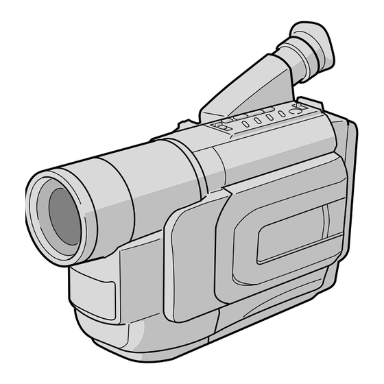
Compact vhs camcorder
Hide thumbs
Also See for GR-FXM38EK:
- Instructions (2 pages) ,
- Service manual (43 pages) ,
- Service manual (83 pages)
Table of Contents
Advertisement
Quick Links
VICTOR COMPANY OF JAPAN, LIMITED
VIDEO DIVISION
SERVICE MANUAL
GR-FXM38EG/EK,SXM48EG/EK/EA
SXM67ED,SXM87ED
SPECIFICATIONS
General
Format
Power source
Power consumption
Viewfinder on
LCD monitor* on
Video light**
* Applicable models only.
** GR-SXM58/SXM48/SX24 only.
Signal system
Video recording system
Luminance
Colour
Cassette
Tape speed
SP
LP
Recording time (max.)
SP
LP
Operating temperature
Operating humidity
Storage temperature
Weight
Dimensions
* Applicable models only.
Pickup
Lens
Viewfinder
White balance adjustment
LCD monitor
(Applicable models only)
S40894
Speaker
(Applicable models only)
Printed in Japan
COMPACT VHS CAMCORDER
(The specifications shown pertain specifically to the model GR-SXM58EK/SXM48EK/FXM38EK/SX24EK/FX14EK)
Connectors
Camcorder
Video (via Video output connector) : 1 V (p-p), 75 W unbalanced, analogue output
Audio (via Audio output connector) : 300 mV (rms), 1 kW analogue output
Digital
: S-VHS (GR-SXM58/SXM48/SX24 only)/VHS PAL standard
(GR-SXM58 only)
: DC 11 V } (Using AC Adapter)
S-Video
DC 6 V } (Using battery pack)
(GR-SXM58/SXM48/SX24 only)
: 4.0 W (GR-SXM58/SXM48/FXM38 only)
3.7 W (GR-SX24/FX14 only)
: 4.5 W (GR-SXM58/SXM48/FXM38 only)
Power requirement
: 3.0 W
Output
: PAL-type
Optional Accessories
: FM recording
: Converted sub-carrier direct recording Conforms to VHS
standard
• Battery Packs BN-V12U, BN-V20U, BN-V400U
:
/
cassette
• Compact S-VHS (
: 23.39 mm/sec.
• Compact VHS (
: 11.70 mm/sec.
• Active Carrying Bag CB-V7U
: 60 minutes
• Cassette Adapter C-P7U
: 120 minutes
(with EC-60 cassette)
: 0°C to 40°C
: 35% to 80%
: –20°C to 50°C
Some accessories are not available in some areas. Please consult your nearest JVC
: Approx. 910 g (GR-SXM58/SXM48 only)
dealer for details on accessories and their availability.
Approx. 900 g (GR-FXM38 only) Approx. 860 g (GR-SX24 only)
Approx. 850 g (GR-FX14 only)
: 200 mm x 112 mm x 118 mm (GR-SXM58/SXM48/FXM38 only)
200 mm x 112 mm x 115 mm (GR-SX24/FX14 only)
(with the LCD monitor* closed and with the viewfinder fully
Specifications shown are for SP mode unless otherwise indicated. E & O.E. Design and
tilted downward)
specifications subject to change without notice.
: 1/6" format CCD
: F1.6, f = 3.9 mm to 62.4 mm,
16:1 power zoom lens with auto iris and macro control, filter
diameter 40.5 mm
: Electronic viewfinder with 0.5" black/white CRT
: Auto/Manual adjustment
: 2.5" diagonally measured, LCD panel/TFT
active matrix system
: Monaural
This service manual is printed on 100% recycled paper.
COPYRIGHT © 2001 VICTOR COMPANY OF JAPAN, LTD.
VHS
PAL
625
: ø3.5 mm, 4-pole, mini-head jack
: Y : 1 V (p-p), 75 Ø, analogue output
C : 0.30 V (p-p), 75 Ø, analogue output
AC Adapter
: AC 110 V — 240 V `, 50 Hz/60 Hz
: DC 11 V } , 1 A
) Cassettes SE-C45/30
) Cassettes EC-60/45/30
No. 86655
November 2001
Advertisement
Table of Contents

Related Manuals for JVC GR-FXM38EK


Summary of Contents for JVC GR-FXM38EK
- Page 1 Operating humidity : 35% to 80% Storage temperature : –20°C to 50°C Some accessories are not available in some areas. Please consult your nearest JVC Weight : Approx. 910 g (GR-SXM58/SXM48 only) dealer for details on accessories and their availability.
-
Page 2: Table Of Contents
3.2.2 Centering ................ 3-2 3.2.3 Vertical scanning ............3-2 3.2.4 Brightness ............... 3-2 3.2.5 Focus ................3-2 The following table lists the differing points between Models GR-FXM38EG, GR-FXM38EK, GR-SXM48EG, GR-SXM48EK, GR-SXM48EA, GR-SXM67ED and GR-SXM87ED in this serise. GR-FXM38EG GR-FXM38EK GR-SXM48EG... -
Page 3: Important Safety Precautions
Important Safety Precautions Prior to shipment from the factory, JVC products are strictly inspected to conform with the recognized product safety and electrical codes of the countries in which they are to be sold. However, in order to maintain such compliance, it is equally important to implement the following precautions when a set is being serviced. - Page 4 • Safety Check after Servicing Examine the area surrounding the repaired location for damage or deterioration. Observe that screws, parts and wires have been returned to original positions, Afterwards, perform the following tests and confirm the specified values in order to verify compliance with safety standards.
-
Page 5: Disassembly
SECTION 1 DISASSEMBLY 1.1 SERVICE CAUTIONS 1.1.3 Connection of the wires 1.1.1 Precautions 1. Pull the connector structure upward to release the clamp when removing or inserting the flat wire cable. 1. Before disassembling/re-assembling the set as well as soldering parts, make sure to disconnect the power ca- ble. -
Page 6: Tools Required For Adjustments
1.2 TOOLS REQUIRED FOR ADJUSTMENTS Alignment tape Alignment tape Service support system PC cable (for SP interchangeability) (for N. SP PB Y/C level) YTU94057-56 QAM0099-002 MHPE-C MHVE-2C Cleaning cloth Torque driver YTU94088 KSMM-01 YTU94088-003 Conn. ring INF adjustment lens Table 1-2-1 YTU92001-111 YTU92001B Gray Scale Chart... -
Page 7: Disassembly/Assembly Of Cabinet Parts
1,2. Alignment tape 1.3 DISASSEMBLY/ASSEMBLY OF CABINET PARTS To be used for check and adjustment of interchange- 1.3.1 Disassembly flow chart ability of the mechanism. This flowchart indicates the disassembly step for the cabi- (Video: Color bar signal, Audio: Non-signal) net parts and board assembly in order to gain access to item(s) to be serviced. -
Page 8: Disassembly Method
1.3.2 Disassembly method REMOVAL STEP *UNLOCK/RELEASE/ Fig. /LOC PART UNPLUG/UNCLAMP/ UNSOLDER CASETTE COVER 2(S1) ASSEMBLY UPPER CASE 2(S2), 2(L2) LOWER CASE 9(S3), (L3a), (L3b) ASSEMBLY *CN3a,CN3b,COVER(JACK) (Incl. E.VF ASSEMBLY) E.VF ASSEMBLY 3(S4) TOP OPERATION 2(S5),(L5a),(L5b),2(L5c), UNIT *CN5a REAR UNIT 3(S6),(L6a),(L6b),*CN6a FRONT COVER 2(S7a),(S7b),(L7a),(L7b), ASSEMBLY... - Page 9 COVER (JACK) Fig. C3 Fig. C4 Fig. C5...
- Page 10 Fig. C6 WITHOUT DC LIGHT MODEL WITH DC LIGHT MODEL Fig. C7...
- Page 11 Fig. C8 BRACKET (UPPER) ASSY ∗ ∗ ∗∗ ∗∗ ∗ : 0.147 N m (1.5 kgf • • ∗∗ : 0.098 N m (1.0 kgf • • Fig. C9...
- Page 12 ∗ UPPER CASE ASSY MONITOR COVER ∗ ∗ ∗ ∗ ∗ ∗ : 0.098 N m (1.0 kgf • • Fig. C10 MONITOR CASE SHIELD CASE LCD MODULE DIFF SHEET BACK LIGHT MONITOR <07> T.HINGE ASSY Fig. C11...
- Page 13 REINFORCED SURFACE PUSH SWITCH ∗ REINFORCED SURFACE COVER (HINGE U) ∗ REINFORCED SURFACE HINGE HINGE NOTE PLATE (SW) ∗∗ COVER (HINGE L) ∗ : 0.049 N m (0.5 kgf • • ∗∗ : 0.078 N m (0.8 kgf • • Fig.
-
Page 14: Disassembly/Assembly Of Camera Section And Deck Section
1.4 DISASSEMBLY/ASSEMBLY OF CAMERA SECTION Reference Notes: AND DECK SECTION <NOTE 1> Destination of connectors 1.4.1 Flowchart of disassembly Note : Two kinds of double-arrows in connection tables The following flowchart shows the disassembly of the cam- respectively show kinds of connector/wires. era section and deck section. - Page 15 SHIELD CASE (MAIN) ∗ ∗ ∗ : 0.108 N m (1.1 kgf • • Fig. D2 Fig. D4 ∗ ∗ ∗ ∗ CUSHION (OP) ∗ : 0.216 N m (2.2 kgf • • Fig. D3 Fig. D5 1-11...
-
Page 16: Replacement Of Ccd Image Sensor
1.5 REPLACEMENT OF CCD IMAGE SENSOR Part Name Orientation Notes: CCD image sensor Mark is on the right viewed as indi- • Pay the most careful attention to the transparent glass and cated by the arrow a . optical LPF of the CCD image sensor so a not the soil and Spacer rubber IC side is horizontal. -
Page 17: Take Out Cassette Tape
1.6 TAKE OUT CASSETTE TAPE 4. While holding down the cassette housing by hand, con- nect the jumper wires to a battery to run the mechanism In the event that the set enters the emergency mode as it to the EJECT position four unloading. If this unloading is loaded with a cassette tape and the cassette tape can- operation is performed as the cassette housing is not not be ejected with the EJECT button, manually, take it out... -
Page 18: Emergency Display
1.7 EMERGENCY DISPLAY Example (in case of the error number E01): Whenever some abnormal signal is input to the mechacon CPU, an error number (E01, as an exam-ple) is displayed in the electronic view finder. In every error status, such the message as shown below al- UNIT IN REMOVE AND ternately appear over and over. - Page 19 Note: 2) As the “DEMO MODE” is executed, the camcoder enters the DEMONSTRATION mode after the ti- tle screen of “TITLE CALL” and “FUTURE” appear in this order. <Flow chart> 1. TITLE CALL and FUTURE ∫ 2. EASY PC CONNECTION ∫...
-
Page 20: Service Note
1.9 SERVICE NOTE 1-16... -
Page 21: Mechanism Adjustment
SECTION 2 MECHANISM ADJUSTMENT 2.1 SERVICE CAUTIONS 2.1.3 Required adjustment tools 2.1.1 Precautions Alignment tape Alignment tape 1. Before disassembling/re-assembling the set as well as MHPE-LC MHPE-C soldering parts, make sure to disconnect the power ca- ble. 2. When disconnecting/connecting connectors, pay enough attention to wiring not to damage it. -
Page 22: Disassembly/Assembly Of Mechanism Parts
2.2 DISASSEMBLY/ASSEMBLY OF MECHANISM PARTS This procedure starts with the condition that the cabinet parts and deck parts. Also, all the following procedures for adjust- ment and parts replacement should be performed in STOP mode. When reassembling, perform the step(s) in the reverse order. - Page 23 <TOP VIEW> Fig. 2-2-1 TOP VIEW <BOTTOM VIEW> Note: When reinstalling the cassette housing to the set, pay careful attention to the switch not to damage it. Fig. 2-2-2 BOTTOM VIEW...
- Page 24 (W1a) (S3a) (W3b) (S3b) (P3) (P1) (W3a) (S1) (W3a) (W1a) (W3a) (W1a) (W1b) (S3a) (S3a) (S3a) (S3a) Fig. M1 Fig. M3 (W2) (S4a) (S4b) (W4) (S4b) (W2) (S2) (W2) Fig. M2 Fig. M4...
- Page 25 (S5a) (S5a) (S7) (S5a) (S5c) (S5b) Fig. M5 Fig. M7 (S6b) (S8) (S8) Catcher (S6d) (W8a) (S6d) (S6d) (S6d) (W8b) (W8b) (S6c) (S6c) (S6a) Fig. M6 Fig. M8...
-
Page 26: Checkup And Adjustment Of Mechanism Phase
2.3 CHECKUP AND ADJUSTMENT OF MECHANISM PHASE Note: Pay careful attention to the installing order and phase of mechanism parts of the loading system. Align the two holes of the Loading ring assembly to those of the deck. Align the hole of the Loading gear (T) assembly to that of the deck. -
Page 27: Tape Transport Adjustment
2.4 TAPE TRANSPORT ADJUSTMENT 8. When the FM waveform breaks in the level varying proc- ess, subtly adjust the height of guide rollers at every In most cases the deck section is in need electrical ad- breaking point so that the waveform varies as flat as pos- justment, it results from replacement of worm mechanical sible. -
Page 28: A/C Head Height & Azimuth
11. Through the above steps, confirm that there occur no 2.4.3 A/C head height & azimuth wrinkling and damage in the tape around the pinch roller 1. Connect the jig connector cable to CN25 on the MAIN and TU guide pole whenever the deck is in operation of board. -
Page 29: Phase Of Control Head (X Value)
2.4.4 Phase of control head (X value) 2.5 REMARKS 1. Connect the jig connector cable to CN25 on the MAIN 2.5.1 Cleaning board. 1. For cleaning of the upper drum (particularly video 2. Playback the SP stairstep signal of the alignment tape heads), use fine-woven cotton cloth or Kimwipe with al- and observe signal at V.TP FM with external trigger from cohol soaks through. -
Page 30: Jig Connector Cable Connection
2.6 JIG CONNECTOR CABLE CONNECTION Remove the cover (JIG). Jig connector cable CN25 Extention connector Cover(JIG) JIG CONNECTOR COMMUNICATION CABLE to 10 pin ( RXD ) to 28 pin ( TXD ) WHITE to 8 or 5 or 4 pin ( GND ) BLACK Fig. -
Page 31: Electrical Adjustment
2 PROM on to new board. Then adjustment are not required. And if parts such as the following need replacement, spe- (LY20701) cial computerized adjustment are required (Refer to sec. 3.1.1- 4). Please contact to JVC Service for detaile informa- Bottom case assy Serial No. label tion. -
Page 32: Electronic Viewfinder (E. Vf) Adjustment
3.2 ELECTRONIC VIEWFINDER (E. VF) ADJUSTMENT 1) Put the deflection yoke to the most inner side of CRT neck first. Then fix the stopper temporary. Notes: 2) Adjust the tilt of picture on the E. VF screen by tilting • Unless otherwise specified, all measurement points and the deflection yoke. -
Page 33: Charts And Diagrams
SECTION 4 CHARTS AND DIAGRAMS 4) Indication on schematic diagram NOTES OF SCHEMATIC DIAGRAM Voltage Indications for REC and PB mode on the sche- matic diagram are as shown below. Safety precautions The Components identified by the symbol critical for safety. For continued safety, replace safety critical components only with manufacturer's recom- REC mode mended parts. -
Page 34: Circuit Board Notes
6. Signal path Symbols CIRCUIT BOARD NOTES The arrows indicate the signal path as follows. 1. Foil and Component sides 1) Foil side (B side) : Playback signal path Parts on the foil side seen from foil face (pattern face) are indicated. -
Page 35: Board Interconnections
∗ BOARD INTERCONNECTIONS NOTE ) : The number of patch cords LCD(MONITOR) MODULE OPEN C_VF_PANEL are indicated by interconnected. E. VF 1 2 3 4 5 6 7 OP BLOCK (Page 4-31) (Page 4-28) CN7602 CN7702 MONITOR (Page 4-29) C-VF C-VF BL ∗... -
Page 36: Cpu Schematic Diagram
NOTES : For the destination of each signal and further line connections that are cut off from CPU SCHEMATIC DIAGRAM this diagram , refer to "4.1 BOARD INTERCONNECTIONS". When ordering parts , be sure to order according to the Part Number indicated in the Parts List. 0 1 MAIN (CPU) TO REG TO A/C HEAD... -
Page 37: M.mda Schematic Diagram
NOTES : For the destination of each signal and further line connections that are cut off from M.MDA SCHEMATIC DIAGRAM this diagram , refer to "4.1 BOARD INTERCONNECTIONS". When ordering parts , be sure to order according to the Part Number indicated in the Parts List. 0 1 MAIN (M.MDA) IC1602 TO REG... -
Page 38: Vtr Asp Schematic Diagram
NOTES : For the destination of each signal and further line connections that are cut off from VTR ASP SCHEMATIC DIAGRAM this diagram , refer to "4.1 BOARD INTERCONNECTIONS". When ordering parts , be sure to order according to the Part Number indicated in the Parts List. JIG_CONN. -
Page 39: Dsp Schematic Diagram
DSP SCHEMATIC DIAGRAM NOTES : For the destination of each signal and further line connections that are cut off from this diagram , refer to "4.1 BOARD INTERCONNECTIONS". When ordering parts , be sure to order according to the Part Number indicated in the Parts List. TO LCD/CVF, BW/CVF 0 1 MAIN (DSP) -
Page 40: F/Z/I/Mda Schematic Diagram
F/Z/I/MDA SCHEMATIC DIAGRAM NOTES : For the destination of each signal and further line connections that are cut off from this diagram , refer to "4.1 BOARD INTERCONNECTIONS". When ordering parts , be sure to order according to the Part Number indicated in the Parts List. 0 1 MAIN (F/Z/I/MDA) IRIS_O/C TO CPU... -
Page 41: Out Schematic Diagram
V OUT SCHEMATIC DIAGRAM NOTES : For the destination of each signal and further line connections that are cut off from this diagram , refer to "4.1 BOARD INTERCONNECTIONS". When ordering parts , be sure to order according to the Part Number indicated in the Parts List. L4701 TO REG 0 1 MAIN (V OUT) -
Page 42: Tg/Cds Schematic Diagram
TG/CDS SCHEMATIC DIAGRAM NOTES : For the destination of each signal and further line connections that are cut off from this diagram , refer to "4.1 BOARD INTERCONNECTIONS". When ordering parts , be sure to order according to the Part Number indicated in the Parts List. TO CCD CN5301 0 1 MAIN (TG/CDS) -
Page 43: Reg Schematic Diagram
C6622 NTSC UDZS8.2B-X Light 0.47 100k SSM3K02F 10µ/16 ∗ ∗ ∗ ∗ ∗ ∗ ∗ ∗ ∗ QGA1201C2-02X JVC WB VF ONLY MODEL UDZS7.5B-X ∗ ∗ ∗ ∗ ∗ Light ∗ ∗ ∗ ∗ ∗ ∗ ∗ ∗ ∗ JVC WB VF and 2.5LCD... -
Page 44: Lcd/Cvf Schematic Diagram
∗ C7064 /6.3 ∗ ∗ C7051 R7114 R7118 R7122 0.01 ∗ C7065 C7066 ∗ y10244001a_rev0 NOTE : The parts with marked ( ) is not used. # : EXCHANGE PARTS LIST JVC MODEL PANA MODEL ∗ CN25 QGB0506L1-30X 4-21 4-22... -
Page 45: Bw/Cvf Schematic Diagram
4.11 BW/CVF SCHEMATIC DIAGRAM NOTES : For the destination of each signal and further line connections that are cut off from this diagram , refer to "4.1 BOARD INTERCONNECTIONS". When ordering parts , be sure to order according to the Part Number indicated in the Parts List. TO DSP BWBLEVEL OPEN... -
Page 46: Jack Schematic Diagram
S OUT 0 1 MAIN (JACK) ∗ NOTE : The parts with marked ( ) is not used. y30154001a_rev0 Exchange Parts List JVC PC JVC NON PC model PANA PC NON S JVC model JVC model PANA JVC model model... -
Page 47: Speaker Schematic Diagram
4.13 SPEAKER SCHEMATIC DIAGRAM NOTES : For the destination of each signal and further line connections that are cut off from this diagram , refer to "4.1 BOARD INTERCONNECTIONS". When ordering parts , be sure to order according to the Part Number indicated in the Parts List. 0 1 MAIN (SPEAKER) C2404 R2401... -
Page 48: Ccd Schematic Diagram
4.14 CCD SCHEMATIC DIAGRAM NOTES : For the destination of each signal and further line connections that are cut off from this diagram , refer to "4.1 BOARD INTERCONNECTIONS". When ordering parts , be sure to order according to the Part Number indicated in the Parts List. IC5301 is incorporated in the CCD base assembly. -
Page 49: Monitor Schematic Diagram
4.15 MONITOR SCHEMATIC DIAGRAM NOTES : For the destination of each signal and further line connections that are cut off from this diagram , refer to "4.1 BOARD INTERCONNECTIONS". When ordering parts , be sure to order according to the Part Number indicated in the Parts List. J7501 NCB21EK-273X C7502... -
Page 50: Vf Schematic Diagram
4.16 E. VF SCHEMATIC DIAGRAM NOTES : For the destination of each signal and further line connections that are cut off from this diagram , refer to "4.1 BOARD INTERCONNECTIONS". When ordering parts , be sure to order according to the Part Number indicated in the Parts List. 6 0 E. -
Page 51: Top Ope Unit, Zoom Unit, Rear Unit And Sensor Schematic Diagrams
4.17 TOP OPE UNIT, ZOOM UNIT, REAR UNIT AND SENSOR SCHEMATIC DIAGRAMS NOTES : For the destination of each signal and further line connections that are cut off from this diagram , refer to "4.1 BOARD INTERCONNECTIONS". The schematic diagram is only for reference. Avoid replacing individual parts. TOP OPE UNIT Replace the entire unit only. -
Page 52: Main Circuit Board
4.18 MAIN CIRCUIT BOARD FOIL SIDE(B) 0 1 MAIN PWB YB10356-01-01 D5201 JP2002 C2001 C5229 L7301 L2003 R122 X102 R5217 C5230 D7301 JP2001 C7316 IC103 Q2001 C126 C7304 C7305 C5231 C7301 R5211 R7315 R7307 C5218 D101 R7305 R7308 R7303 Q7306 R7327 R2004 C7315... - Page 53 COMPONENT PARTS LOCATION GUIDE <MAIN/YB10356-01-01> (1/2) REF.NO. LOCATION REF.NO. LOCATION REF.NO. LOCATION REF.NO. LOCATION REF.NO. LOCATION REF.NO. LOCATION REF.NO. LOCATION D6701 L6201 CAPACITOR C2004 C4037 C5234 C7068 L6301 C2005 C4038 C5235 C7069 D6702 C103 L6302 C2021 C4039 C5236 C7301 D7301 C104 C2022 C4040...
- Page 54 (2/2) COMPONENT PARTS LOCATION GUIDE <MAIN/YB10356-01-01> REF.NO. LOCATION REF.NO. LOCATION REF.NO. LOCATION REF.NO. LOCATION REF.NO. LOCATION REF.NO. LOCATION REF.NO. LOCATION Q7013 R163 R3507 R4505 R6610 R7312 TL1606 Q7015 R164 R3508 R4507 R6611 R7313 TL1607 Q7301 R165 R3901 R4508 R6612 R7315 TL1608 Q7303 R166...
- Page 55 COMPONENT SIDE(A) 0 1 MAIN PWB YB10356-01-01 R7333 Q7311 Q9201 ZP33-14 CN22 R7332 Q9203 ZP33-16 F7301 CN9013 R7331 CN9012 C4047 CN13 IC102 R7330 C107 C1630 ZP13-6 R9204 R9209 C5227 R3501 R9207 ZP12-3 C5234 C111 RA109 C5228 C5209 L7304 ZP13-5 ZP13-7 ZP13-10 R5215 R7309...
-
Page 56: Monitor Circuit Board
4.19 MONITOR CIRCUIT BOARD 0 7 MONITOR PWB 0 7 MONITOR PWB FOIL SIDE(B) COMPONENT SIDE(A) YB20913 YB20913 J7501 R7620 L7605 R7621 R7622 R7624 R7625 R7630 R7626 C7627 R7629 R7627 R7628 IC7603 L7601 C7620 C7602 R7642 C7619 C7601 C7626 T7501 R7636 Q7607 Q7605... -
Page 57: Ccd Circuit Board
4.20 CCD CIRCUIT BOARD FOIL SIDE(B) 0 2 CCD PWB YB10356-01-01 IC5301 CL5301 COMPONENT SIDE(A) 0 2 CCD PWB YB10356-01-01 C5305 C5301 C5302 C5307 4-43... -
Page 58: Vf Circuit Board
4.21 E. VF CIRCUIT BOARD FOIL SIDE(B) 6 0 E. VF PWB Q7003 R7023 R7029 R7019 VR7002 R7024 IC7001 C7013 R7025 R7021 Q7001 R7016 R7008 R7030 C7005 R7020 R7006 R7005 R7010 COMPONENT SIDE (A) 6 0 E. VF PWB L7002 VR7003 CN7002 5.5M... -
Page 59: Waveforms
4.22 WAVEFORMS — VTR ASP — IC3501-21 IC3501-25 IC3501-19 IC3501-20 REC 0.1 Vp-p REC 0.57 Vp-p 24 mVp-p 0.24 Vp-p 2 mV/10 µsec/DIV 10 mV/10 µsec/DIV 1 mV/5 msec/DIV 20 mV/5 msec/DIV — DSP — IC4001-160 IC4001-161 IC4001-146 IC4001-147 REC/PB 0.28 Vp-p REC 0.52 Vp-p REC/PB 0.28 Vp-p REC 0.15 Vp-p... -
Page 60: Voltage Charts
4.23 VOLTAGE CHARTS <M.MDA> <CPU> MODE MODE MODE MODE MODE PLAY PLAY PLAY PLAY PLAY PIN NO. PIN NO. PIN NO. PIN NO. PIN NO. IC101 IC103 IC1601 IC104 IC105 11.1 11.1 10.3 10.3 IC1801 Q101 11.1 11.1 11.1 11.1 10.3 10.3 Q102... - Page 61 MODE MODE MODE MODE MODE PLAY PLAY PLAY PLAY PLAY PIN NO. PIN NO. PIN NO. PIN NO. PIN NO. Q3501 1(E) 2(B) IC1602 3(C) 4(E) 5(B) 6(C) Q3502 1(E) Q1601 2(B) 3(C) 11.1 11.1 4(E) 5(B) 6(C) Q3505 <VTR ASP> MODE REC PLAY PIN NO.
- Page 62 MODE MODE MODE MODE MODE PLAY PLAY PLAY PLAY PLAY PIN NO. PIN NO. PIN NO. PIN NO. PIN NO. IC4202 Q4251 Q4501 <V OUT> MODE PLAY PIN NO. IC4701 IC4702 IC4501 IC4003 Q4701 Q4702 Q4001 IC4002 <TG/CDS> MODE PLAY PIN NO.
- Page 63 <CCD> <E.VF> <MONITOR> MODE MODE MODE MODE MODE MODE MODE MODE MODE MODE MODE PLAY PLAY PLAY PLAY PLAY PIN NO. PIN NO. PIN NO. PIN NO. PIN NO. PIN NO. PIN NO. PIN NO. PIN NO. PIN NO. PIN NO. 14.9 14.9 11.1...
-
Page 64: Power System Block Diagram
4.24 POWER SYSTEM BLOCK DIAGRAM REAR UNIT MAIN REG SECTION M. MDA SECTION DRM_PWR Q6401 L6002 UNREG DRM_PWR DRUM POWER L6001 CAP_PWR F6001 CN28 DRM_CTL BATT_+ CAP_PWR BATT_+ IC6001-6,39PIN Q6501 UNREG M_UNREG REG_3.2V ADP_DC UNREG POWER CAPSTAN ADP_DC F6002 ADP_H M_UNREG MOTOR ADP_H... -
Page 65: Cpu/Mda System Block Diagram
4.25 CPU/MDA SYSTEM BLOCK DIAGRAM MAIN (CPU) (M. MDA) IC101(CPU) IC1601 DRUM ROTOR POSI CENTER POSITION IC103 RTC CS (RTC) AL SI START UP TIMMING SWITCHING DRUM CLK CONTROL CONTROL SCLK AL CLK D COIL U OSCIN D COIL U FORWARD DRUM ON C1617... -
Page 66: Camera And Y/C System Block Diagram
4.26 CAMERA AND Y/C SYSTEM BLOCK DIAGRAM 0 2 CCD MAIN V_PB_C IC5201 (TG/CDS) IC4001(DSP) (DSP) (CDS/AGC/AD) IC5301 Q5301 CN5301 CN22 OPTICAL CCD_OUT CDSIN γ BLKSH PROCESS BLOCK CONV CLAMP γ T. G SEPA DSP CONTROL BLKFB (3LINE) OFFSET CDS_CLK INTER FACE SERIAL INTERFACE ADCLK... - Page 67 JIG_CONN. CN25 J504 A/V OUT V_PB_C IC4001(DSP) J505 S OUT IC4701 DA_R (V OUT) ∗ DA_B IC4702 Y/C MIX TO LCD/CVF &6dB AMP (V OUT) Q3502 IC3501 DA_G CH2_S (VTR ASP) PB AMP TO BW/CVF CH2_F BWY0 BWYOUT Q3502 Q4701 Q4702 PB AMP CH4_S...
-
Page 68: Monitor System Block Diagram
4.27 MONITOR SYSTEM BLOCK DIAGRAM LCD MONITOR T7501 T7501 MONITOR FROM REG CN16 CN7601 F7501 F7501 REG_4.8V REG_4.8V REG_4.8V Q7503 Q7503 Q7501 Q7501 Q7504 Q7504 Q7502 Q7502 FROM CPU CN7602 LCD_CTL L7604 LCD_CTL REG_15V L7601 REG_3.2V MREG_4.8V VSS(REG_-15V) REG_3.2V CLK1 CLK1 IC7602 R7607... -
Page 69: Parts List
QPA02003506 POLY BAG,A,B,C,E,G,H,J,K,L MODEL MARK YQM30061-3 POLY BAG,D,F LYT0860-002A INST.BOOK(GE),B,K GR-FXM38EG-X LYT0860-002B INST.BOOK(GE),A,E GR-FXM38EG-Y LYT0860-003B INST.BOOK(FR),A,E GR-FXM38EG-Z LYT0860-004B INST.BOOK(DU),A,E LYT0860-005B INST.BOOK(SP),A,E GR-FXM38EK LYT0860-006B INST.BOOK(IT),A,E GR-SXM48EG-X LYT0860-007A INST.BOOK(DA),B,K GR-SXM48EK LYT0860-008A INST.BOOK(FI),B,K LYT0860-009A INST.BOOK(SW),B,K GR-SXM48EA LYT0860-010A INST.BOOK(NO),B,K GR-SXM67ED LYT0860-011A INST.BOOK(RU),C,L LYT0860-012A INST.BOOK(CZ),C,L... - Page 70 FINAL ASSEMBLY <M2> ELECTRONIC VIEWFINDER <M4> MAIN <01> 140C 110B 140A MECHANISM <M3> 140D 140E 110A 140E 140D 110D 110C 140F 140B 140B 110E RATING 110F LABEL <02> 159A 101B 251C 135E 135H OPTICAL BLOCK 135E 251C SECTION 101D 101E 135E 135K 135J...
-
Page 71: Final Assembly
REF No. PART No. PART NAME, DESCRIPTION REF No. PART No. PART NAME, DESCRIPTION - - - - - - - - - - - - - - - - - - - - - - - - - - - - - - - - - - - - - - - - - - - - - - - - - - - - - - - - - - - - - - - - - - - - - - - - - - - - - - - - - - - - - - - - - - - - - - - - - - - - - - - - - - - - - - - - - - - - - - - - - - - - - - - - - - - -... -
Page 72: Mechanism Assembly
BEWARE OF BOGUS PARTS Parts that do not meet specifications may cause trouble in regard to safety MECHANISM ASSEMBLY <M3> and performance. We recommend that genuine JVC parts be used. 469A 469B 469B 439A 425 425 429A 406B 406A Classification Part No. - Page 73 REF No. PART No. PART NAME, DESCRIPTION REF No. PART No. PART NAME, DESCRIPTION - - - - - - - - - - - - - - - - - - - - - - - - - - - - - - - - - - - - - - - - - - - - - - - - - - - - - - - - - - - - - - - - - - - - - - - - - - - - - - - - - - - - - - - - - - - - - - - - - - - - - - - - - - - - - - - - - - - - - - - - - - - - - - - - - - - -...
-
Page 74: Electronic Viewfinder Assembly
ELECTRONIC VIEWFINDER ASSEMBLY <M4> ELECTRONIC VIEWFINDER <60> 357A SERIAL NO. LABEL REF No. PART No. PART NAME, DESCRIPTION REF No. PART No. PART NAME, DESCRIPTION - - - - - - - - - - - - - - - - - - - - - - - - - - - - - - - - - - - - - - - - - - - - - - - - - - - - - - - - - - - - - - - - - - - - - - - - - - - - - - - - - - - - - - - - - - - - - - - - - - - - - - - - - - -... -
Page 75: Monitor Assembly
MONITOR ASSEMBLY <M5> 502B 502A 502D 502D 502C 502E 503B 503A MONITOR 501B <07> 503C 501D 501C 501A REF No. PART No. PART NAME, DESCRIPTION REF No. PART No. PART NAME, DESCRIPTION - - - - - - - - - - - - - - - - - - - - - - - - - - - - - - - - - - - - - - - - - - - - - - - - - - - - - - - - - - - - - - - - - - - - - - - - - - - - - - - - - - - - - - - - - - - - - - - - - - - - - - - - - - -... -
Page 76: Electrical Parts List
GR-SXM87ED GR-FXM38EG-Y GR-SXM48EK GR-SXM48EG-Y ELECTRICAL PARTS LIST GR-FXM38EG-Z GR-SXM48EA GR-SXM48EG-Z GR-FXM38EK GR-SXM67ED REF No. PART No. PART NAME, DESCRIPTION REF No. PART No. PART NAME, DESCRIPTION - - - - - - - - - - - - - - - -... - Page 77 REF No. PART No. PART NAME, DESCRIPTION REF No. PART No. PART NAME, DESCRIPTION - - - - - - - - - - - - - - - - - - - - - - - - - - - - - - - - - - - - - - - - - - - - - - - - - - - - - - - - - - - - - - - - - - - - - - - - - - - - - - - - - - - - - - - - - - - - - - - - - - - - - - - - - - - - - - - - - - - - - - - - - - - - - - - - - - - -...
- Page 78 REF No. PART No. PART NAME, DESCRIPTION REF No. PART No. PART NAME, DESCRIPTION - - - - - - - - - - - - - - - - - - - - - - - - - - - - - - - - - - - - - - - - - - - - - - - - - - - - - - - - - - - - - - - - - - - - - - - - - - - - - - - - - - - - - - - - - - - - - - - - - - - - - - - - - - - - - - - - - - - - - - - - - - - - - - - - - - - -...
- Page 79 REF No. PART No. PART NAME, DESCRIPTION REF No. PART No. PART NAME, DESCRIPTION - - - - - - - - - - - - - - - - - - - - - - - - - - - - - - - - - - - - - - - - - - - - - - - - - - - - - - - - - - - - - - - - - - - - - - - - - - - - - - - - - - - - - - - - - - - - - - - - - - - - - - - - - - - - - - - - - - - - - - - - - - - - - - - - - - - -...
- Page 80 REF No. PART No. PART NAME, DESCRIPTION REF No. PART No. PART NAME, DESCRIPTION - - - - - - - - - - - - - - - - - - - - - - - - - - - - - - - - - - - - - - - - - - - - - - - - - - - - - - - - - - - - - - - - - - - - - - - - - - - - - - - - - - - - - - - - - - - - - - - - - - - - - - - - - - - - - - - - - - - - - - - - - - - - - - - - - - - -...
- Page 81 REF No. PART No. PART NAME, DESCRIPTION REF No. PART No. PART NAME, DESCRIPTION - - - - - - - - - - - - - - - - - - - - - - - - - - - - - - - - - - - - - - - - - - - - - - - - - - - - - - - - - - - - - - - - - - - - - - - - - - - - - - - - - - - - - - - - - - - - - - - - - - - - - - - - - - - - - - - - - - - - - - - - - - - - - - - - - - - -...
-
Page 82: Ccd Board Assembly <02
REF No. PART No. PART NAME, DESCRIPTION REF No. PART No. PART NAME, DESCRIPTION - - - - - - - - - - - - - - - - - - - - - - - - - - - - - - - - - - - - - - - - - - - - - - - - - - - - - - - - - - - - - - - - - - - - - - - - - - - - - - - - - - - - - - - - - - - - - - - - - - - - - - - - - - - - - - - - - - - - - - - - - - - - - - - - - - - -... -
Page 83: E.vf Board Assembly <60
REF No. PART No. PART NAME, DESCRIPTION REF No. PART No. PART NAME, DESCRIPTION - - - - - - - - - - - - - - - - - - - - - - - - - - - - - - - - - - - - - - - - - - - - - - - - - - - - - - - - - - - - - - - - - - - - - - - - - - - - - - - - - - - - - - - - - - - - - - - - - - - - - - - - - - - - - - - - - - - - - - - - - - - - - - - - - - - -...
Need help?
Do you have a question about the GR-FXM38EK and is the answer not in the manual?
Questions and answers