
Related Manuals for QRP Labs QMX+


Summary of Contents for QRP Labs QMX+
- Page 1 QMX+ QMX+ QRP Labs Multimode Xcvr (transceiver) Assembly manual --- PCB Rev 1 --- QMX+ assembly Rev 1.00...
-
Page 2: Table Of Contents
Contents Contents..................................2 1. Introduction.................................3 2. Assembly..................................5 2.1 General guidelines..............................5 2.2 PCB diagrams (trace, component identification)....................8 2.3 Parts list................................14 2.4 Inventory of parts..............................19 2.5 Install all the ceramic capacitors..........................21 2.6 Install 1N4007 diodes............................23 2.7 Install 47uH inductors............................24 2.8 Install BS170 PA transistors..........................25 2.9 Assemble and install transformer T501.......................26 2.10 Wind and install L502............................28 2.11 Wind and install Band Pass Filter toroids L401, L403-L405................29... -
Page 3: Introduction
Optional internal GPS module for setting real-time clock and frequency discipline for WSPR • operation Lifetime free firmware upgrades with QRP Labs Firmware Update (QFU) bootloader for • easy firmware update on any OS with no extra software, or drivers, or programming... - Page 4 PLEASE READ THE BASIC ASSEMBLY AND USE INSTRUCTIONS IN THIS MANUAL VERY CAREFULLY BEFORE APPLYING POWER TO THE BOARD! IMPORTANT! QMX+ can be built for 9V or 12V operation! You need to decide NOW! A 9V QMX+ produces 5 W power output from a supply voltage of 9V or a little over. At 12V, a QMX+ built for 9V could be producing 8 W power output which is likely to cause over-heating and perhaps failure of the BS170 final transistors.
-
Page 5: Assembly
Assembly 2.1 General guidelines Assembly of this kit is quite straightforward, but very detailed; most components are SMD and have already been pre-assembled by the PCB factory. The usual kit-building recommendations apply: work in a well-lit area, with peace and quiet to concentrate. Some of the other semiconductors in the kit are sensitive to static discharge. - Page 6 Tracks shown in BLUE are on the bottom layer. Tracks shown in RED are on the top layer. One internal layer is used mainly for transporting digital and analog signals relatively long-distance on the board, and these traces are shown in YELLOW. One layer is used primarily (but not exclusively) for power rails (12V, 5V, 3.3V).
- Page 7 Hidden or buried via: neither ends of the via are visible on either surface; the via transitions signals entirely between internal layers only. Unfortunately a 6-layer board is much more expensive than a 2-layer board; and if you use blind or hidden vias the costs escalate even more drastically.
-
Page 8: Pcb Diagrams (Trace, Component Identification)
Tips for a successful build: 1. READ the manual, and every instruction carefully! Don’t try to be a hero (proceed without reading carefully). There are many more people who will need to buy a new board, than real heroes… 2. Don’t rush! Take your time! 3. - Page 9 QMX+ Main board: QMX+ assembly Rev 1.00...
- Page 10 QMX+ Main board layout, top side: QMX+ assembly Rev 1.00...
- Page 11 QMX+ Main board layout, bottom side: QMX+ assembly Rev 1.00...
- Page 12 QMX+ Front panel board traces: QMX+ Front panel board: QMX+ assembly Rev 1.00...
- Page 13 QMX+ Connectors board: QMX+ SMPS boards Trace layout: Top side components: Bottom side components: QMX+ assembly Rev 1.00...
-
Page 14: Parts List
2.3 Parts list Component nomenclature is by schematic sheet. Part numbers Power supply boards, schematic page 1 • Main board, CPU etc., schematic page 2 • LCD board and controls board, schematic page 3 • Main board, receiver section, schematic page 4 •... - Page 15 Capacitors (50V, Multi-layer Ceramic capacitors except where indicated otherwise) Value Description Component numbers 2.2u SMD 0603 C101 C102 C103 C104 C105 C215 C216 C406 C407 C408 C413 C414 C430 C434 C444 C510 470u 10V tantalum C106, C107, C504 0.1u SMD 0603 C201, C202, C203, C206, C207, C208, C209, C210, C211, C212, C214, C217, C219, C409, C410, C415, C428, C429, C436, C438, C445, C501, C503, C507,...
- Page 16 Semiconductors Description Component numbers SMD: 1N4148 SOD323 D101 D102 D103 D104 D105 D501 D505 D506 D507 D516 SMD: SS14 DO-214AC D106 D107 D502 D514 D515 1N4007 diode D508, D509, D510, D511, D512, D513, D517, D518, D519, D520, D521 SMD: 5.6V 5W SMB D108 SMD: 3.6V 500mW SOD-123 D109...
- Page 17 Description Component numbers BN61-202 binocular, 3:3 T501 BN43-1502 binocular T507 T50-2 (red) L401 T37-6 (yellow) L403, L506, L508, L511, L512 T37-17 (yellow/blue) L404, L405b, L510, L513 T37-0 (pink) L405a, L515, L516, L517, L518, L519, L520 Miscellaneous Value Description 2.1 mm DC 2.1 x 5.5 barrel DC power connector USB C USB type C connector...
- Page 18 Enclosure (OPTIONAL) Value Description Top/Bottom Extruded aluminium top/bottom (identiical parts) Front panel Laser etched drilled/cut (display, controls, connectors) Rear panel Laser etched, drilled (connectors) M3 machine screw Screws to secure end panels Rubber foot Self-adhesive rubber foot QLG3 GPS (OPTIONAL) Value Description PCB Assembly...
-
Page 19: Inventory Of Parts
2.4 Inventory of parts Note: Capacitor colours vary depending on availability. All are NP0/C0G Class-I RF dielectric. QMX+ assembly Rev 1.00... - Page 20 QMX+ assembly Rev 1.00...
-
Page 21: Install All The Ceramic Capacitors
2.5 Install all the ceramic capacitors There are 32 through-hole capacitors in accordance with the following table and diagram. The procedure is so easy that I have included all capacitors in a single assembly step rather than doing one diagram for each capacitor value. Nevertheless be very careful to insert the correct value capacitors in the correct places. - Page 22 QMX+ assembly Rev 1.00...
-
Page 23: Install 1N4007 Diodes
2.6 Install 1N4007 diodes Install the 12 1N4007 diodes D508-D513 and D517-522. Pay attention to the orientation of the diodes which is critically important. The diodes have a black body and a white stripe. The PCB silkscreen arrows point towards the white stripe (diode cathode) end. But the white silkscreen arrow on the PCB can be hard to see. -
Page 24: Install 47Uh Inductors
2.7 Install 47uH inductors Install the eight 47uH axial inductors L504, L505, L507, L509, L514, L521, L522 and L523.. These axial through-hole inductors are all installed lying flat on the PCB. Bend each lead at 90-degrees carefully, near the inductor body, and the wires should then be correctly spaced to fit the holes on the board. -
Page 25: Install Bs170 Pa Transistors
2.8 Install BS170 PA transistors Install the four BS170 transistors in the positions shown, with their flat faces flush against the PCB. Use the 10mm M3 steel bolt, washer and nut to firmly press the transistor faces against the PCB, as shown. -
Page 26: Assemble And Install Transformer T501
2.9 Assemble and install transformer T501 Transformer T501 is wound on the large binocular ferrite former, using the thick 0.6mm (AWG #22) wire. This wire is also used for L502 and T507 so do not use all of it on the transformer. Please refer to the separate document that describes the preparation of this transformer. - Page 27 Cut the wire-endings to a length of about 2mm on the underside of the board and solder them with plenty of heat, time and solder. Now check for DC continuity with a DVM between all the points marked A in the photograph above.
-
Page 28: Wind And Install L502
2.10 Wind and install L502 L502 consists of 10 turns of 0.6mm (AWG #22) wire wound on an FT37-43 toroid (dull black colour). Firstly, you have to understand that there’s a right way and a wrong way to wind a toroidal inductor, too. -
Page 29: Wind And Install Band Pass Filter Toroids L401, L403-L405
2.11 Wind and install Band Pass Filter toroids L401, L403-L405 Unlike on QMX where there is one single T50-sized toroids with multiple taps producing four Band Pass Filters, in QMX there are five toroids, each having a single tap, and this makes a total of eight BPFs. Using one toroid with one tap per two BPFs makes it much easier to optimize performance without getting unwanted... - Page 30 Start winding with the wire coming in from the left, over the top of the toroidal core, and down through the hole, out to the right. You continue to fill up the toroid windings anti-clockwise around the core. The start of the winding will henceforth be indicated with 0.
- Page 31 nearest the line of capacitors, as indicated. The tap goes into the hole marked ‘19’ at the top right of the toroid, and the end of the winding goes into the hole marked ‘30’ which is near the middle of the toroid.
-
Page 32: Install Low Pass Filter Toroids
This diagram illustrates the two toroids installed vertically on the position of L405. Which way around the toroids goes doesn’t matter (which wire is considered the “start” and which the “end”); arrange it whichever way seems neatest to you. 2.12 Install Low Pass Filter toroids There are 12 Low Pass Filter toroids, all wound using the 0.33mm (AWG #28) enameled wire. - Page 33 QMX+ assembly Rev 1.00...
-
Page 34: Wind And Install Trifilar Toroid T401
2.13 Wind and install trifilar toroid T401 This toroid needs some care so please follow these instructions very carefully. Cut three 20cm lengths of 0.33mm (AWG #28) wire. These three pieces now need to be tightly twisted together to make the trifilar wire. My method for this is to tie one end in a knot around a small screwdriver shaft. - Page 35 Hold the core between thumb and finger. Pass the wire first from above, to below. Then take the wire from below, and bring it around to pass through the toroid again to form the second turn. After each turn, ensure the wire is fitting snugly around the toroidal core. Wind 10 turns on the core. Each time through the toroid’s central hole counts as one turn.
- Page 36 wires to 2mm length then the toroid is more likely to fall out before you’ve had a chance to solder any of the wires. If that happens, it will be tough to get all the wires back in the correct holes again. Be careful when soldering the wires of toroid T401, NOT to touch any of the nearby SMD components! Once again my method involves holding the iron and plenty of solder on the joint for at least 10 seconds to make sure the enamel burns off completely.
-
Page 37: Wind And Install Transformer T507
2.14 Wind and install transformer T507 Cut two lengths of 0.33mm wire, each approximately 25cm long. Wind 10 turns through each hole of the BN43-1502 binocular core. Cut two 25mm lengths of 0.60mm wire. These are threaded only ONCE through each hole. The transformer is installed as shown on the diagram. -
Page 38: Install Rear Panel Connectors
2.15 Install rear panel connectors Install the four rear panel connectors as follows (USB-C is already SMD assembled): X101: DC Power connector • X201: 3.5mm jack: PTT output • X218: 3.5mm jack: AUX connection • X502: BNC RF connector – NOTE: there is a footprint for an SMA connector that you may •... -
Page 39: Install Right-Angle Front Panel Pin Header Connectors
2.16 Install right-angle front panel pin header connectors Install the following 90-degree male pin header connectors: 2x4-pin 90-degree male header connector JP215 • 2x4-pin 90-degree male header connector JP216 • 2x3-pin 90-degree male header connector JP201 • Be careful to ensure that the pin headers are accurately aligned, they should sit square in the PCB, with the pins matching the silkscreen legend, not at a slightly twisted angle. -
Page 40: Install Power Supply Boards
2.17 Install power supply boards To complete the assembly of the main board, install the power supply boards. This is a little tricky and needs to be done with care to ensure that the board connectors all sit square and at the right height etc. - Page 41 This photograph shows the final installation of the 3.3V (upper) and 5V (lower) SMPS boards, so you know what you’re working toward: 3. Fit power supply boards: Fit the power supply boards over the protruding 10mm M3 nylon screws, and thread on another nylon nut on the top side of each board. Tighten it carefully by turning the screws from below the board.
- Page 42 4. 2x4-pin and 3-pin header connections: Find the 2x4-pin male 90-degree pin header and matching female connector sockets, and the corresponding 2x3-pin connectors. Cut about 1mm from each pin of the female pin header connectors. The pins have a square cross- section.
- Page 43 alignment before soldering the others. If you have an adjustable iron: lower the temperature. Solder quickly so as not to melt the plastic of the connectors. Be careful not to damage nearby SMD components or create any shorts or solder bridges! Inspect with the jeweller’s loupe! Don’t panic if things seem slightly out of alignment, it will probably be OK, and it is difficult to make it 100% perfect.
-
Page 44: Install Audio And Paddle Connectors
2.18 Install Audio and Paddle connectors The audio and paddle connectors are 3.5mm stereo jack sockets of the same type as the AUX and PTT out connectors on the rear panel. They need to be installed on their own small PCB, which is attached to the main PCB using the capacitor wire off-cuts you kept from earlier. - Page 45 This small connectors PCB has ten connecting holes to the bottom left corner of the main board. You will insert capacitor offcut wires into these holes and solder on each side, to fix the connector board to the main PCB. It’s very important that the connectors PCB must be UNDER the main PCB.
-
Page 46: Install R305 Contrast Trimmer Potentiometer
2.19 Install R305 contrast trimmer potentiometer This trimmer is installed on the BACK (bottom) side of the front panel PCB! Be very careful to solder this on the correct (front) side of the PCB, it will be very difficult to remove afterwards if you get it wrong now. -
Page 47: Install Cr2032 Battery Holder
2.21 Install CR2032 battery holder The CR2032 battery holder is an SMD component which is easily soldered by hand. Just a blob of solder on the terminals suffices. Correct orientation is ensured by observing the cut-off corner and making sure it is at the bottom left: critical for correct battery polarity! 2.22 Install microphone The microphone is installed on the front side of the front panel PCB. -
Page 48: Install Push-Button Switches S302 And S303
2.23 Install push-button switches S302 and S303 Install the push-buttons on the front side of the PCB. When soldering on the rear, holding the soldering iron on the side of each pin nearest the middle of the switch will avoid melting the adjacent pin headers. -
Page 49: Assemble Front Panel And Lcd
2.25 Assemble front panel and LCD The following steps assume that you are installing the QMX+ in the optional enclosure. It’s easier to complete this assembly BEFORE soldering the LCD module. If you are not going to install the QMX+ in the optional enclosure, then follow the same steps but without the aluminium front panel itself. - Page 50 Step 4: Thread on the LCD module as shown. Note the orientation: the 16 connection pads are at the “top” edge of the front panel, therefore the silkscreen printing on the module is “upside down”. The holes in the LCD module are only just sufficiently large to accommodate the M3 (3mm) screw. It may be necessary to turn the screw with a screwdriver to encourage the screw through one or more of the holes.
- Page 51 Step 6: Insert the 16-pin male pin header strip into the LCD module connector pads. The pin header has a short pin side and a long pin side. It will be easiest to insert the short pin side into the LCD module pads as shown. Step 7: Thread the front panel PCB onto the four screws as shown, taking care that the 16-pin header correctly goes into the LCD module on one side, and the main PCB on the other: QMX+ assembly Rev 1.00...
- Page 52 Step 8: Add four nylon nuts to the four black screws and tighten them with the needle nose pliers. Do not over tighten! It’s only nylon, not your enemy’s neck. Tightening these nuts is very easy in three out of the four cases; the difficult one is the bottom left nut, whose hexagonal corners will interfere with the 2x3-pin header each 60-degrees of rotation.
- Page 53 Step 10: Now you can solder the two unsoldered pins of the “Tune” rotary encoder. Relish the odor of molten nylon as you burn the plastic nut (in other words, please solder quickly – and try to avoid touching the plastic with the iron tip). For bonus points you may wish to use a DVM in continuity mode to check that the top pin is grounded (the mid pin of the opposite three is also ground), but there is NO continuity from the bottom pin to ground.
-
Page 54: Add The Button Caps And Knobs
Step 12: In what will now seem like a practically trivial step, complete the front panel assembly by soldering the remaining 16 pins of the LCD from the rear side of the front panel: 2.26 Add the button caps and knobs You can now add the button caps, which should be firmly pushed onto the button shaft, and the knobs. -
Page 55: Final Enclosure Assembly
2.27 Final enclosure assembly If your rear PCB happens to be still fixed to the rear panel by the nut of the BNC connector, for the purposes of alignment, it will best to detach this now. This is because a certain amount of wriggling is likely required to put together the various sub-assemblies, and this is easiest WITHOUT the rear panel at this stage. - Page 56 Step 3: Fix on the rear panel using the BNC connector nut: Step 4: Remember: practically, you will want to power-up, make adjustments such as the LCD contrast trimmer, etc., BEFORE finally screwing together the case. But for completeness… To finish the radio, add the top half of the enclosure; make sure it is the correct way round, remember the enclosure walls have a U-groove on one side and an I-tongue on the other.
-
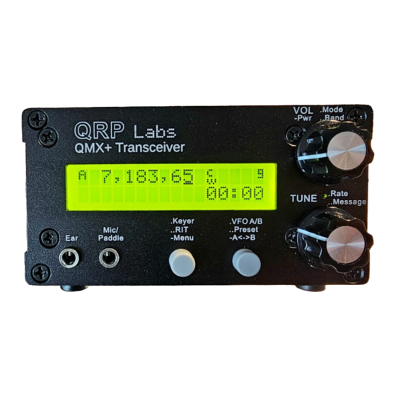
Page 57: Qmx+ Front Panel Connections
2.28 QMX+ front panel connections The QMX+ front panel has two 3.5mm connectors, labeled “Ear” and “Mic/Paddle”. The “Ear” connector is the audio output, intended to drive standard 32-ohm earphones, though many types of headphones will also be suitable. The “Mic/Paddle” connector has dual purpose. A standard Morse paddle may be connected; if the “dit”... - Page 58 • on-screen if you have configured it. The GPS produces two output signals, PPS (Pulse-per-second) and RxD (Serial data). A GPS such as the QRP Labs QLG2 is perfect for use as an external GPS module (see http://qrp- labs.com/ql g2 ) or you may use the internal QLG3 module.
- Page 59 It should be noted that: The QRP Labs 50W PA may not be used in high duty cycle modes such as FT8, JS8 etc at • full power. It should be de-rated to half power operation at maximum, by using a 12V or 13.8V supply.
-
Page 60: Final Checks Before Applying Power The First Time
WARNING: QRP Labs recommends a maximum supply voltage of 12.0V for QMX+, which is particularly important when running high duty-cycle digital operations. Do NOT use a battery with a nominal 12V voltage, which may in fact be much higher when fully charged. -
Page 61: Connections For Basic Operation
A 2.1mm DC connector plug is required; the center pin is + and the barrel is ground (negative). WARNING: QRP Labs recommends a maximum supply voltage of 12.0V for QMX+, which is particularly important when running high duty-cycle digital operations. -
Page 62: Firmware Installation
QMX+ will do anything at all. On occasion QRP Labs will make available updated firmware for QMX+, in order to deliver bug fixes or functionality enhancements. Firmware updates are always freely available to all QMX+ owners, and may be downloaded from the QMX+ web page http://qrp-labs.com/QMX+... - Page 63 Exiting bootloader (firmware update) mode: QMX+ provides two possible ways to exit firmware update mode: 1) Update the firmware! After updating the firmware, QMX+ will automatically reboot in normal operating mode. 2) Power down QMX+, and re-apply the power again. QMX+ will reboot in normal operating mode (as long as a valid firmware file has been installed, at least the first time you use QMX+).
- Page 64 Or copy and paste it, however you wish. The file on the QRP Labs website is a ZIPPED file, please be sure to unzip it to get the .QMX+ file before copying it to QMX+.
- Page 65 The encrypted QMX+ firmware file will only work on a QRP Labs QMX+ board, it cannot be • installed on any other board, even one containing the same processor. No other firmware file will work on the QRP Labs QMX+ board except an official QRP Labs •...
-
Page 66: Qlg3 Gps Option
3. QLG3 GPS option The QLG3 is an internal GPS module option specifically designed for the QMX+. The GPS module itself is E108, the same as used on the general purpose QLG2 module. However this minimalist QLG3 PCB for the QMX+ contains no logic level conversion, indicators, voltage regulator, or USB- Serial converter. - Page 67 Step 4: Mount the two 11mm hex nylon spacers on the main QMX+ PCB, using a 6mm nylon screw tightened from the bottom side of the main QMX+ PCB. Step 5: Crucially, the VBAT pin of the E108 module needs to be powered; there are two options: Power it from the normal +3.3V Vdd supply rail.
-
Page 68: Dev Kit Option
4. Dev kit option The Dev kit consists of a matrix board, four 11mm nylon hex spacers, and 8 M3 6mm screws. The screws and spacers may be used with any four of the available 7 holes on the main QMX PCB to mount the Dev board 11mm above the main QMX+ board. -
Page 69: Resources
5. Resources For updates and tips relating to this kit please visit the QRP Labs QMX+ kit page http://qrp- labs.com/QMX+ For any questions regarding the assembly and operation of this kit please join the QRP Labs group, see http://qrp-labs.com/group...
Need help?
Do you have a question about the QMX+ and is the answer not in the manual?
Questions and answers