Table of Contents
Advertisement
Quick Links
UHF FM Transceiver
VX-427A (LTR
Service Manual
©
2009 VERTEX STANDARD CO., LTD.
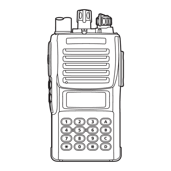
16 key Version
This transceiver was assembled using Pb (lead) free solder, based on the RoHS specification.
Only lead-free solder (Alloy Composition: Sn-3.0Ag-0.5Cu) should be used for repairs performed on this appara-
tus. The solder stated above utilizes the alloy composition required for compliance with the lead-free specification,
and any solder with the above alloy composition may be used.
Specifications ..........................................................2
Exploded View & Miscellaneous Parts ..............3
Block Diagram ......................................................... 5
Circuit Description ................................................7
Alignment ................................................................9
®
)
Series
EC071U95C
Introduction
This manual provides technical information necessary for ser-
vicing the VX-427A (LTR
Servicing this equipment requires expertise in handling surface-
mount chip components. Attempts by non-qualified persons to
service this equipment may result in permanent damage not cov-
ered by the warranty, and may be illegal in some countries.
Two PCB layout diagrams are provided for each double-sided
circuit board in the transceiver. Each side of is referred to by the
type of the majority of components installed on that side ("lead-
ed" or "chip-only"). In most cases one side has only chip com-
ponents, and the other has either a mixture of both chip and lead-
ed components (trimmers, coils, electrolytic capacitors, ICs, etc.),
or leaded components only.
While we believe the technical information in this manual to be
correct, VERTEX STANDARD assumes no liability for dam-
age that may occur as a result of typographical or other errors
4 key Version
that may be present. Your cooperation in pointing out any in-
consistencies in the technical information would be appreciated.
Important Note
Contents
VERTEX STANDARD CO., LTD.
4-8-8 Nakameguro, Meguro-Ku, Tokyo 153-8644, Japan
VERTEX STANDARD
US Headquarters
10900 Walker Street, Cypress, CA 90630, U.S.A.
YAESU UK LTD.
Unit 12, Sun Valley Business Park, Winnall Close
Winchester, Hampshire, SO23 0LB, U.K.
VERTEX STANDARD HK LTD.
Unit 5, 20/F., Seaview Centre, 139-141 Hoi Bun Road,
Kwun Tong, Kowloon, Hong Kong
VERTEX STANDARD ( AUSTRALIA ) PTY., LTD.
Normanby Business Park, Unit 14/45 Normanby Road
Notting Hill 3168, Victoria, Australia
) Series FM Transceiver.
®
LTR
is a registered trademark of E.F Johnson Company.
®
Board Unit (Schematics, Layouts & Parts)
MAIN-2 Unit ............................................................ 25
DUMMY Unit .......................................................... 51
Optional Units (Schematics, Layouts & Parts)
FVP-25 Encryption / DTMF Pager Unit .............. 52
1
Advertisement
Table of Contents

Subscribe to Our Youtube Channel
Related Manuals for Vertex Standard LTR VX-427A Series


Summary of Contents for Vertex Standard LTR VX-427A Series
-
Page 1: Table Of Contents
(trimmers, coils, electrolytic capacitors, ICs, etc.), or leaded components only. While we believe the technical information in this manual to be correct, VERTEX STANDARD assumes no liability for dam- age that may occur as a result of typographical or other errors 16 key Version 4 key Version that may be present. -
Page 2: Specifications
Specifications General Frequency Range: 450-490 MHz Number of Systems: Number of Groups: Channel Spacing: 12.5 / 25 kHz PLL Steps: 5 / 6.25 kHz Power Supply voltage: 7.5 VDC ± 10% Operating Temperature Range: –22°F to +140°F (–30°C to +60°C) Frequency Stability: ±2.5 ppm Dimensions (WHD):... -
Page 3: Exploded View & Miscellaneous Parts
Exploded View & Miscellaneous Parts RA0545500 CP8656001 WINDOW FRONT CASE ASSY (16 key) (W/ LIGHT GUIDE, NAME PLATE, SP NET, SPEAKER, PACKING PAD, RA0545300 PTT KNOB, SHEET(MIC), CR SPONGE RUBBER, WINDOW ASSY) DOUBLE FACE TAPE (LCD) RA0173500 R6147510 RING NUT (x 2 pcs) RA0810500 KNOB ASSY (256CH) CP8656002... - Page 4 Note...
-
Page 5: Block Diagram
Block Diagram... - Page 6 Note...
-
Page 7: Circuit Description
Circuit Description Receive Signal Path The resulting DC squelch control voltage is passed to Incoming RF from the antenna jack is delivered to the pin 19 of the microprocessor Q2047 (LC87F74C8A). If MAIN-2 Unit and passes through a low-pass filter con- no carrier is received, this signal causes pin 19 of Q2047 sisting of coils L2001, L2002, and L2003, capacitors to go high and pin 30 to go low. - Page 8 Circuit Description (2SC5005), pre driver amplifier Q2020 (2SC3357), section of Q2051. There the VCO signal is divided by 64 driver amplifier Q2014 (RD01MUS1), and then the am- or 65, according to a control signal from the data latch plified transmit signal is applied to the final amplifier section of Q2051, before being sent to the programmable Q2008 (RD07MVS1), which delivers up to 5 watts of divider section of Q2051.
-
Page 9: Alignment
Note: Signal levels in dB referred to in this procedure are by the warranty policy. Also, Vertex Standard must re- based on 0 dBμ = 0.5 μV (closed circuit). serve the right to change circuits and alignment proce- dures in the interest of improved performance, without notifying owners. - Page 10 Alignment Set up the test equipment as shown below for trans- PLL VCV (Varactor Control Voltage) ceiver alignment, and apply 7.5V DC power to the trans- Connect the DC voltmeter between TP2045 on the ceiver. Main Unit and ground. Set the transceiver to CH 4 (high band edge), and ad- Power Supply just L2036 on the Main Unit for 4.0 V ±...
- Page 11 Alignment The Alignment Tool Outline Reference Frequency Install the VX-427A Programming Software to your Set the transceiver to CH 1 (band center) via the “Chan- nel” box on the “Alignment” window previously. Execute the VX-427A Programming Software. Click the left mouse button on the “Reference Fre- Click the left mouse button on the “Radio”...
- Page 12 Alignment Transmitter Output Power Set the transceiver to CH 1 (band center) via the “Chan- Click the left mouse button on the “Power Low” but- ton. nel” box on the “Alignment” window previously. Click the left mouse button on the “Power High” but- Click the left mouse button on the “Start”...
- Page 13 Alignment Max Deviation Set the transceiver to CH 1 (band center, wide devia- Set the transceiver to CH 2 (band center, narrow de- viation) via the “Channel” box on the “Alignment” win- tion) via the “Channel” box on the “Alignment” win- dow previously.
- Page 14 Alignment CTCSS Deviation Set the transceiver to CH 1 (band center, wide devia- Set the transceiver to CH 2 (band center, narrow de- viation) via the “Channel” box on the “Alignment” win- tion) via the “Channel” box on the “Alignment” win- dow previously.
- Page 15 Alignment Modulation Balance Note: Do not apply the microphone input in this adjust- Set the transceiver to CH 2 (band center, narrow de- viation) via the “Channel” box on the “Alignment” win- ment. Set the transceiver to CH 1 (band center, wide devia- dow.
- Page 16 Alignment DCS Deviation Set the transceiver to CH 1 (band center, wide devia- Set the transceiver to CH 2 (band center, narrow de- viation) via the “Channel” box on the “Alignment” win- tion) via the “Channel” box on the “Alignment” win- dow previously.
- Page 17 Alignment LTR Deviation Set the transceiver to CH 1 (band center, wide devia- Set the transceiver to CH 2 (band center, narrow de- viation) via the “Channel” box on the “Alignment” win- tion) via the “Channel” box on the “Alignment” win- dow previously.
- Page 18 Alignment Sequential Tone Deviation STD Deviation Set the transceiver to CH 1 (band center, wide devia- Set the transceiver to CH 1 (band center, wide devia- tion) via the “Channel” box on the “Alignment” win- tion) via the “Channel” box on the “Alignment” win- dow previously.
- Page 19 Alignment RX Tune ( Sensitivity ) Tight Noise Squelch Set the transceiver to CH 1 (band center, wide devia- Set the transceiver to CH 1 (band center, wide devia- tion) via the “Channel” box on the “Alignment” win- tion) via the “Channel” box on the “Alignment” win- dow previously.
- Page 20 Alignment Threshold Noise Squelch Set the transceiver to CH 2 (band center, narrow de- Set the transceiver to CH 1 (band center, wide devia- viation) via the “Channel” box on the “Alignment” win- tion) via the “Channel” box on the “Alignment” win- dow.
- Page 21 Alignment Tight Noise Squelch RSSI Set the transceiver to CH 2 (band center, narrow de- Set the transceiver to CH 1 (band center, wide devia- viation) via the “Channel” box on the “Alignment” tion) via the “Channel” box on the “Alignment” win- window.
- Page 22 Alignment TX Save RSSI Set the transceiver to CH 2 (band center, narrow de- Set the transceiver to CH 1 (band center, wide devia- viation) via the “Channel” box on the “Alignment” tion) via the “Channel” box on the “Alignment” win- window.
- Page 23 Alignment Set the transceiver to CH 2 (band center, narrow de- This completes the alignment routine. Press the “Exit” box to save all settings and close the “Alignment” window, viation) via the “Channel” box on the “Alignment” win- dow. then turn the radio off. Tune the RF output of the Radio Tester to 470.100 MHz, then set the output level to +15 dBμ...
- Page 24 Note...
-
Page 25: Main-2 Unit
MAIN-2 Unit (Lot. 1 ~ 3) Circuit Diagram... - Page 26 MAIN-2 Unit (Lot. 1 ~ 3) Note...
- Page 27 MAIN-2 Unit (Lot. 1 ~ 3) Parts Layout (Side A) BR93L86RFVM-WTR 2SA1602A (MF) BD4835FVE (DR) DTA144EE (16) IMZ2A (Z2) LMV321IDCKR (R3x) 12-22SURSYGC/S530-A2/TR8 (Q2036) (Q2004) (Q2040) (Q2039) (Q2003) (Q2064) (D2039) NJM12904R (Q2054) LC87F7BC8A (Q2047) NJM2070M 2SC4154E (LE) CPH6102 (AB) DTC114TE (04) UMX1N (X1) DA221 (K) (Q2005)
- Page 28 MAIN-2 Unit (Lot. 1 ~ 3) Parts Layout (Side B) HSM88AS (C1) (Lot. 2~) (D2044) DAN222 (N) (D2025, 2026) DA221 (K) (D2036) DA221M (K) (D2044) NJM2871AF35 AK2342BP MB15A01PFV1 TC7W74FU RD01MUS1 2SK508 (K52) 2SA1586GR (SY) 2SC4116GR (LG) CPH6102 (AB) DTB123EK (F12) DTC124TE (05) UMX1N (X1) (Q2021)
- Page 29 MAIN-2 Unit (Lot. 4 ~ 9) Circuit Diagram...
- Page 30 MAIN-2 Unit (Lot. 4 ~ 9) Note...
- Page 31 MAIN-2 Unit (Lot. 4 ~ 9) Parts Layout (Side A) BR93L86RFVM-WTR 2SA1602A (MF) BD4835FVE (DR) DTA144EE (16) IMZ2A (Z2) LMV321IDCKR (R3x) 12-22SURSYGC/S530-A2/TR8 (Q2036) (Q2004) (Q2040) (Q2039) (Q2003) (Q2064) (D2039) (Q2066:Lot. 4~) NJM12904R (Q2054) LC87F7BC8A (Q2047) NJM2070M 2SC4154E (LE) CPH6102 (AB) DTC114TE (04) UMX1N (X1) DA221 (K)
- Page 32 MAIN-2 Unit (Lot. 4 ~ 9) Parts Layout (Side B) HSM88AS (C1) (D2044: Lot. 2~) DAN222 (N) (D2025, 2026) DA221 (K) (D2036) DA221M (K) (D2044: Lot. 1) NJM2871AF35 AK2342BP MB15A01PFV1 TC7W74FU RD01MUS1 2SK508 (K52) 2SA1586GR (SY) 2SC4116GR (LG) CPH6102 (AB) DTB123EK (F12) DTC124TE (05) UMX1N (X1)
- Page 33 MAIN-2 Unit (Lot. 10 ~) Circuit Diagram...
- Page 34 MAIN-2 Unit (Lot. 10 ~) Note...
- Page 35 MAIN-2 Unit (Lot. 10 ~) Parts Layout (Side A) BR93L86RFVM-WTR 2SA1576A (F) BD4835FVE (DR) DTA144EE (16) IMZ2A (Z2) LMV321IDCKR (R3x) 1LTST-S326KGJRKT (Q2036) (Q2004, 2066) (Q2040) (Q2039) (Q2003) (Q2064) (D2039) NJM12904R (Q2054) LC87F7BC8A (Q2047) NJM2070M 2SC4081 (B) CPH6102 (AB) DTC114TE (04) UMX1N (X1) DA221 (K) (Q2005)
- Page 36 MAIN-2 Unit (Lot. 10 ~) Parts Layout (Side B) HSM88AS (C1) (D2044) DAN222 (N) (D2025, 2026) DA221 (K) (D2036) DA221M (K) (D2044) NJM2871AF35 AK2342BP MB15A01PFV1 TC7W74FU RD01MUS1 2SK508 (K52) 2SA1576A (F) 2SC4081 (B) CPH6102 (AB) DTB123EK (F12) DTC124TE (05) UMX1N (X1) (Q2021) (Q2051) (Q2062)
- Page 37 MAIN-2 Unit Parts List REF. DESCRIPTION VALUE TOL. MFR’S DESIG VXSTD P/N VERS. LOT. SIDE LAY ADR PCB with Components CS1925001 16 KEY, IS OFF CS1925002 4 KEY, IS OFF CS1925003 16 KEY, IS ON CS1925004 4 KEY, IS ON Printed Circuit Board FR015350A FR015350B...
- Page 38 MAIN-2 Unit Parts List REF. DESCRIPTION VALUE TOL. MFR’S DESIG VXSTD P/N VERS. LOT. SIDE LAY ADR C 2062 CHIP TA.CAP. 10uF TEESVB21C106M8R K78120025 NON IS C 2063 CHIP CAP. 0.001uF GRM155B11H102KA01D K22178809 C 2065 CHIP CAP. 15pF GRM1552C1H150JZ01D K22178216 C 2066 CHIP CAP.
- Page 39 MAIN-2 Unit Parts List REF. DESCRIPTION VALUE TOL. MFR’S DESIG VXSTD P/N VERS. LOT. SIDE LAY ADR C 2129 CHIP CAP. 0.0047uF GRM36B472K25PT K22148830 C 2129 CHIP CAP. 0.0047uF GRM155B11H472KA01D K22178838 C 2131 CHIP CAP. 6.3V GRM188B10J105KA01D K22084801 C 2132 CHIP CAP.
- Page 40 MAIN-2 Unit Parts List REF. DESCRIPTION VALUE TOL. MFR’S DESIG VXSTD P/N VERS. LOT. SIDE LAY ADR C 2192 CHIP CAP. 220pF GRM36CH221J25PT K22148203 C 2192 CHIP CAP. 220pF GRM1552C1H221JA01D K22179713 C 2194 CHIP CAP. 0.5pF GRM1554C1HR50BZ01D K22178285 C 2195 CHIP CAP.
- Page 41 MAIN-2 Unit Parts List REF. DESCRIPTION VALUE TOL. MFR’S DESIG VXSTD P/N VERS. LOT. SIDE LAY ADR C 2262 CHIP CAP. 82pF GRM1552C1H820JD01D K22178234 C 2263 CHIP CAP. 39pF GRM1552C1H390JZ01D K22178226 C 2264 CHIP CAP. 0.0047uF GRM36B472K25PT K22148830 C 2264 CHIP CAP.
- Page 42 Parts List REF. DESCRIPTION VALUE TOL. MFR’S DESIG VXSTD P/N VERS. LOT. SIDE LAY ADR D 2019 DIODE 1SS400G T2R G2070934 D 2020 DIODE DA221 TL G2070178 D 2021 DIODE HVD350B KRF-E G2070946 D 2022 DIODE HVD350B KRF-E G2070946 D 2023 DIODE HVD350B KRF-E G2070946...
- Page 43 MAIN-2 Unit Parts List REF. DESCRIPTION VALUE TOL. MFR’S DESIG VXSTD P/N VERS. LOT. SIDE LAY ADR L 2020 COIL 0.018uH AS030421-18NK L0022584 L 2021 M.RFC 0.068uH HK1608 68NJ-T L1690526 L 2022 M.RFC 0.22uH ELJ-NDR22JF L1690628 L 2023 M.RFC 0.22uH ELJ-NDR22JF L1690628 L 2024...
- Page 44 MAIN-2 Unit Parts List REF. DESCRIPTION VALUE TOL. MFR’S DESIG VXSTD P/N VERS. LOT. SIDE LAY ADR Q 2034 TRANSISTOR 2SC4081 T106 R G3340818R Q 2035 TRANSISTOR DTC114TE TL G3070225 Q 2036 BR93L86RFVM-WTR G1094242 Q 2037 TRANSISTOR 2SC4154-T111-1E G3341548E Q 2037 TRANSISTOR 2SC4081 T106 R G3340818R...
- Page 45 Parts List REF. DESCRIPTION VALUE TOL. MFR’S DESIG VXSTD P/N VERS. LOT. SIDE LAY ADR R 2032 CHIP RES. 1/16W 5% RMC1/16S 101JTH J24189013 R 2033 CHIP RES. 1/16W 5% RMC1/16 221JATP J24185221 R 2034 CHIP RES. 1/16W 5% RMC1/16 221JATP J24185221 R 2035 CHIP RES.
- Page 46 MAIN-2 Unit Parts List REF. DESCRIPTION VALUE TOL. MFR’S DESIG VXSTD P/N VERS. LOT. SIDE LAY ADR R 2100 CHIP RES. 1/16W 5% RMC1/16S 103JTH J24189037 R 2101 CHIP RES. 2.2k 1/16W 5% RMC1/16S 222JTH J24189029 R 2102 CHIP RES. 1/16W 5% RMC1/16S JPTH J24189070...
- Page 47 MAIN-2 Unit Parts List REF. DESCRIPTION VALUE TOL. MFR’S DESIG VXSTD P/N VERS. LOT. SIDE LAY ADR R 2164 CHIP RES. 1/16W 5% RMC1/16S 103JTH J24189037 R 2165 CHIP RES. 1/16W 5% RMC1/16S 102JTH J24189025 R 2166 CHIP RES. 1/16W 5% RMC1/16S 181JTH J24189016 R 2167...
- Page 48 MAIN-2 Unit Parts List REF. DESCRIPTION VALUE TOL. MFR’S DESIG VXSTD P/N VERS. LOT. SIDE LAY ADR R 2227 CHIP RES. 1/16W 5% RMC1/16S JPTH J24189070 R 2228 CHIP RES. 1/16W 5% RMC1/16S 102JTH J24189025 R 2229 CHIP RES. 8.2k 1/16W 5% RMC1/16S 822JTH J24189036...
- Page 49 MAIN-2 Unit Parts List REF. DESCRIPTION VALUE TOL. MFR’S DESIG VXSTD P/N VERS. LOT. SIDE LAY ADR R 2297 CHIP RES. 1/16W 5% RMC1/16S 181JTH J24189016 16KEY R 2298 CHIP RES. 1/16W 5% RMC1/16S 181JTH J24189016 R 2298 CHIP RES. 1/16W 5% RMC1/16S 181JTH J24189016 16KEY...
- Page 50 MAIN-2 Unit Note...
-
Page 51: Dummy Unit
DUMMY Unit Circuit Diagram Parts Layout Lot. 1~2 Lot. 3~ Parts List REF. DESCRIPTION VALUE TOL. MFR’S DESIG VXSTD P/N VERS. LOT. SIDE LAY ADR PCB with Components CB3674001 Printed Circuit Board FR002510C FR002510D C 4001 CHIP CAP. 0.0018uF GRM39B182M50PT K22174812 C 4002 CHIP CAP. -
Page 52: Fvp-25 Encryption / Dtmf Pager Unit
FVP-25 Encryption / DTMF Pager Unit Circuit Diagram Parts Layout Side A Side B M64026FP LC73881 DTC144EU (26) (Q1001) (Q1002) (Q1003) - Page 53 FVP-25 Encryption / DTMF Pager Unit Parts List REF. DESCRIPTION VALUE TOL. MFR’S DESIG VXSTD P/N VERS. LOT. SIDE LAY ADR *** FVP-25 *** Printed Circuit Board FR005010F C 1001 CHIP CAP. 0.1uF GRM39B104K16PT K22124805 C 1002 CHIP CAP. 0.01uF GRM39B103M25PT K22144802 C 1003 CHIP CAP.
- Page 54 Copyright 2009 VERTEX STANDARD CO., LTD. All rights reserved No portion of this manual may be reproduced without the permission of VERTEX STANDARD CO., LTD.
Need help?
Do you have a question about the LTR VX-427A Series and is the answer not in the manual?
Questions and answers