Table of Contents
Advertisement
ELECTRONICS
This Service Manual is a property of Samsung Electronics Co.,Ltd.
Any unauthorized use of Manual can be punished under applicable
international and/or domestic law.
© Samsung Electronics Co., Ltd. DEC. 2006
Printed in Korea
AK82- 01201A
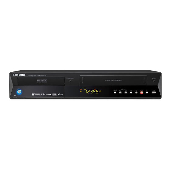
DVD-VCR Recorder COMBO
Chassis : Nexus (4th Generation)
BASIC : DVD- VR357
Application Models
: DVD-VR357 / DVD-VR355 /
Application Areas
:
SERVICE
DVD-VCR RECORDER COMBINATION
DVD-VR350
XAA, XAC, XAX
Manual
Merit & Character regarding Product
ΠSuper Multi Fomat Recoding
DVD- RAM/ DVD± R/ VDV± R
´ Multi Format Playback
DVD/ DVD- RAM/ DVD± RW/ DVD± R
CD/ CD- R/ CD- RW/ MP3/ JPEG
ˇ Recording Mode
XP( 1Hour)/ SP( 2Hour)/ LP( 4Hour)/ EP( 6~ 8Hour)
¨ Progressive Scan
Both DVD & VCR
ˆ Automatic Chapter Product ON
Ø Quick Recoding
Advertisement
Table of Contents

Related Manuals for Samsung DVD-VR357


Summary of Contents for Samsung DVD-VR357
- Page 1 ˆ Automatic Chapter Product ON Ø Quick Recoding © Samsung Electronics Co., Ltd. DEC. 2006 This Service Manual is a property of Samsung Electronics Co.,Ltd. Printed in Korea Any unauthorized use of Manual can be punished under applicable international and/or domestic law.
- Page 2 IMPORTANT SERVICE GUIDE ◆ MODE SWITCH (PROGRAM SWITCH) ASSEMBLY POINT 1) When installing the ass’y deck on the Main PCB, be sure to align the assembly point of mode switch. Œ REMOVE 4 SCREWS When installing the ass'y full deck on the Main PCB, be sure to align the assembly point of mode switch.
-
Page 3: Table Of Contents
CONTENTS 1. Precautions 1-1 ~ 1-6 1-1 Safety Precaution (1-1) 1-2 Servicing Precautions (1-3) 1-3 ESD Precautions (1-4) 1-4 Handling the optical pick-up (1-5) 2. Product Specification 2-1 ~ 2-8 2-1 Product Specification (2-1) 2-2 Chassis Product Specification (2-2) 2-3 Option Product Specification (2-7) 3. - Page 4 CONTENTS 8. Electrical Parts List 8-1 ~ 8-20 9. Block Diagrams 9-1 ~ 9-10 9-1 All Block Diagram (DVD-VR357) (9-2) 9-2 AIC1(PCM1753) Audio DA Block Diagram (9-3) 9-3 AIC9(PCM1802) Audio AD Block Diagram (9-4) 9-4 DIC1(S5L3200) A/V Codec Block Diagram...
- Page 5 CONTENTS 12-12 Audio (DVD Main PCB) (12-14) 12-13 Main Connector (DVD Main PCB) (12-15) 12-14 Video Decoder (DVD Main PCB) (12-16) 12-15 HDMI (DVD Main PCB) (12-17) 12-16 HDMI CEC (DVD Main PCB) (12-18) 12-17 AV Out (DVD Main PCB) (12-19) 12-18 Front (Function PCB) (12-20)
- Page 6 Metal Part cal return path to the chassis. Any current measured must not exceed 0.5mA. Reverse the instrument power cord plug in the out- ohmmeter let and repeat the test. See Fig. 1-1. Fig. 1-2 Insulation Resistance Test Samsung Electronics...
- Page 7 (5) antenna wiring. Always inspect in all areas tinuously and new instructions are issued whenev- for pinched, out-of-place, or frayed wiring, Do not er appropriate. change spacing between a component and the printed-circuit board. Check the AC power cord for damage. Samsung Electronics...
-
Page 8: Precautions 1-1
Components identi- fied by shading, by( ) or by ( ) in the circuit dia- gram are important for safety or for the characteris- tics of the unit. Always replace them with the exact replacement components. Samsung Electronics... -
Page 9: Esd Precautions
(6) Do not remove a replacement ESD device from its protective package until immediately before your are ready to install it.(Most replacement ESD devices are packaged with leads electrically short- ed together by conductive foam, aluminum foil or comparable conductive materials). Samsung Electronics... -
Page 10: Handling The Optical Pick-Up
◆ Be sure to put on a wrist strap grounded to the sheet. ◆ Be sure to lay a conductive sheet made of copper etc. Which is grounded to the table. Samsung Electronics... - Page 11 Precautions MEMO Samsung Electronics...
-
Page 12: Product Specification 2-1
Picture compression format MPEG-II Audio compression format Dolby digital 2ch/256kbps Recording Qallity XP(about 8Mbps), SP(about 4Mbps), LP(about 2Mbps), EP(about 1.2Mbps) Video S/N Ratio Min. 50dB at standard recording Audio S/N Ratio MIN. 75dB Audio frequency characteristics 20Hz ~ 20KHz Samsung Electronics... -
Page 13: Chassis Product Specification
Product Specification 2-2 Chassis Product Specification Model Name(Buyer Model Name) DVD-VR335 DVD-VR357 / VR355 / VR350 Export Country USA / USA / CANADA Buyer Name SEA / SEA / SECA Production TSEC TSEC Genera Instruction Manual ( Language ) Eng / Eng / Eng/Fra OSD/OSP - Language (RED ;... - Page 14 Product Specification Model Name(Buyer Model Name) DVD-VR335 DVD-VR357 / VR355 / VR350 10key (for Ch Select) Multi-Brand TV Control SYSTEM TERMINALS (IN /OUT) Video/Audio In RCA Jack (on the Front) Yes (LINE 2) x1 Yes (LINE 2) x1 S-Video Input (on the Rear)
- Page 15 Product Specification Model Name(Buyer Model Name) DVD-VR335 DVD-VR357 / VR355 / VR350 Narrow Head Yes (19µ) Yes (19µ) Tape Speed NTSC : REC, (PB) SP / EP , (SP / LP / EP) SP / EP , (SP / LP / EP) FEATURES Index Function ( Search &...
- Page 16 Product Specification Model Name(Buyer Model Name) DVD-VR335 DVD-VR357 / VR355 / VR350 Super Audio CD (HD Layer) Super Audio CD (CD Layer) Copy Controled CD DISC TEXT Memory Stick (ATRAC3) Memory Stick (JPEG) VIDEO Video DAC 54MHz/10Bit 54MHz/10Bit Progressive (P480)
- Page 17 Product Specification Model Name(Buyer Model Name) DVD-VR335 DVD-VR357 / VR355 / VR350 ACCESSORIES Remote Controller Batteries Power Cord Type EP-2 Polarity EP-2 Polarity Plug Conversion Euro Scart Cable(21pin) RF Cable No / No / Yes RCA Audio Cable RCA A/V Cable...
-
Page 18: Option Product Specification
Product Specification 2-3 Option Product Specification Description Fig Description Parts No Remark Remote Model Standard of AK59-00062A Control DVD-VR357/XAA Model Standard of Batteries for AC43-12002H DVD-VR357/XAA Remote Control S.N.A Model Standard of AK68-01287A User’s Manual DVD-VR357/XAA Model Standard of DVD-VR357/XAA... - Page 19 Product Specification MEMO Samsung Electronics...
-
Page 20: Alignment And Adjustments 3-1
- Intermittently short-circuit the Test Point on VCR-Jack PCB with pincers to the adjustment mode. - If the corresponding adjustment button is pressed, the adjustment is performed automatically. - When the adjustment is completed, be sure to turn the power off. 3-1-1(a) Location of adjustment button of remote control Fig. 3-1 Samsung Electronics... - Page 21 Alignment and Adjustments 3-1-1(b) TEST location for adjustment mode setting Short-Circuit for few seconds and release. (Just one time) Fig. 3-2 VCR-Jack PCB (Top View) Samsung Electronics...
- Page 22 <Table 3-1 NVRAM Option Table> MODEL OPTION NUMBERS DVD-VR357/XAA 2, 5, 7, 9, 12, 13, 20, 21, 25, 26, 31, 32, 33, 34, 35, 37, 38 DVD-VR355/XAA 2, 5, 7, 9, 13, 20, 21, 25, 26, 31, 32, 33, 34, 35, 37, 38...
-
Page 23: Vcr Mechanical Adjustment
Fig. 3-5 Location of Tape Transport Adjustment PINCH ROLLER FE HEAD CYLINDER ASS'Y GUIDE ROLLER "S" GUIDE ROLLER "T" POST TENSION #8 GUIDE POST #9 GUIDE POST #3 GUIDE POST MAIN BASE ACE HEAD CAPSTAN SHAFT Fig. 3-6 Tape Travel Diagram Samsung Electronics... - Page 24 TI LT SCREW SCREW (D) X-POSITION LOCKING X-POSITION ADJUST SLIT SCREW (B) AZIMUTH ADJUST Fig. 3-7 Location of AC Head Adjustment Screw AUDIO HEAD VIDEO HEAD 0 ~ 0 .25 mm CONTROL HEAD Fig. 3-8 AC Head Height Adjustment Samsung Electronics...
- Page 25 Fig. 3-9 Tape Guide Check c. AUDIO AZIMUTH ADJUSTMENT 1) Load alignment tape (Mono scope) and playback the 7KHz signal. 2) Connect channel-1 scope probe to audio output. 3) Adjust screw (B) to achieve maximum audio level. (See Fig. 3-7) Samsung Electronics...
- Page 26 5) Insert the (-) driver into the X-Point adjustment hole and adjust it so that envelope waveform is maximum. Test point : TP2 (Audio Output) TP3 (Envelope) TP (H’D S/W -Trigger) TP5 (Control Pulse) AUDIO OUTPUT ENVELOPE HEAD SWITCHING CONTRO PULSE Fig. 3-10 Location of Test point (VCR-Jack PCB-Top View) Samsung Electronics...
- Page 27 5) If the section B in Fig. 3-15 does not meet the specification, adjust the guide roller T up or down. a b c d c,b,d/a Fig. 3-11 Envelope Waveform Adjustment H'D SWITCHING PULSE ENVELOPE Fig. 3-12 Adjustment Points Samsung Electronics...
- Page 28 ) driver to obtain a flat video RF envelope as shown in Fig. 3-13. IDEAL ENVELOPE S HEIGHT TOO HIGH T HEIGHT TOO HIGH S HEIGHT TOO LOW T HEIGHT TOO LOW GUIDE ROLLER S GUIDE ROLLER T Fig. 3-13 Guide Roller S, T Height Adjustment Samsung Electronics...
- Page 29 2) If excessive tape wrinkle is observed, perform the following adjustments in Playback mode : ◆ Tape wrinkle at the guide roller S, T section : Linearity adjustment. ◆ Tape wrinkle at tape guide flange : AC head assembly coarse adjustment. Samsung Electronics 3-10...
- Page 30 4) Transportation of accurate driving force is done by gears. (Gear Center Ass’y) Note : If the spec. does not meet the followings specifications, replace the holder clutch ass’y and then recheck. <Table 3-2> MODE TORQUE g/cm GAUGE 2 ± 11 Cassette Torquemeter 15 ± 30 Cassette Torquemeter 3-11 Samsung Electronics...
- Page 31 Alignment and Adjustments MEMO Samsung Electronics 3-12...
-
Page 32: Software Update 4-1
4. Software Update 4-1 Drive Firmware Update 4-1-1 Introduction Samsung will often support software update to improve the performance of DVD Recorder&VCR to the latest staus, through Samsung Internet Site. (www. samsung.com) 4-1-2 How to make an update disc • Write the downloaded file onto a blank CD-R or CD-RW disc, using the following settings : 1) You have to download a newl file through Samsung lnternet site. - Page 33 Drive Firmware is successfully updated. Fig. 4-4 Fig. 4-5 6) After removing the update disc, turn off the unit with power button. Afterwards turn unit back on with power button to close file. The drive firmware is now completed. Samsung Electronics...
-
Page 34: Flash Update
Software Update 4-2 Flash Update 4-2-1 Introduction Samsung will often support software update to improve the performance of DVD Recorder&VCR to the latest staus, through Samsung Internet Site. (www. samsung.com) 4-2-2 How to make an update disc Write the downloaded file onto a blank CD-R or CD-RW disc, using the following settings : 1) You have to download a newl file through Samsung lnternet site. - Page 35 The message below will be displayed in the screen after update is completed and the tray will open automatically. * If the message to the left isn’t displayed after 10minutes and the unit is no longer functioning properly, contact a samsung authorized service center. Flash Update Flash memory is successfully updated.
-
Page 36: Disassembly And Reassembly 5-1
5-1-2 Ass’y Bottom Cover Removal Fig. 5-3 Ass’y Front Panel Removal(Top View) (Bottom View) ´ REMOVE 3 HOOKS ´ REMOVE 10 SCREWS (Bottom View) (3 * 10 WHITE) Fig. 5-4 Ass’y Front Panel Removal(Bottom View) Fig. 5-2 Ass’y Bottom Cover Removal Samsung Electronics... - Page 37 ¨ REMOVE 1 SCREW CBC PCB ˇ REMOVE 4 SCREWS (3 * 10 BLK) ´ REMOVE 4 SCREWS (3 * 12 YELLOW) (DVD-VR357 Only) (3 * 12 YELLOW) VCR DECK DVD DECK Ø REMOVE 1 SCREW Œ REMOVE 2 SCREWS...
-
Page 38: Circuit Board Locations
Disassembly and Reassembly 5-2 Circuit Board Locations VCR JACK PCB HDMI PCB CBC PCB (VR357 Only) DVD MAIN PCB FUNCTION PCB Fig. 5-7 Circuit Board Locations Samsung Electronics... -
Page 39: Vcr Deck Parts Locations
5-3 VCR Deck Parts Locations 5-3-1 Top View ´ Œ ˇ ¨ ˆ Ø Fig. 5-8 Top parts Location-1 Œ GEAR FL CAM ´ ASS’Y MOTOR LOADING ˇ ASS’Y LEVER ARM ¨ ASS’Y HOLDER CASSETTE ˆ LEVER DOOR Ø SLIDER FL DRIVE Samsung Electronics... - Page 40 ´ ASS’Y CYLINDER ˝ GEAR IDLE ˇ ASS’Y CE HEAD Ô LEVER IDLE ¨ ASS’Y LEVER UNIT PINCH ASS’Y LEVER T BRAKE ˆ ASS’Y LEVER #9 GUIDE Ò DISK T REEL Ø ASS’Y LEVER TENSION ∏ ASS’Y BAND BRAKE Samsung Electronics...
- Page 41 Œ GEAR JOINT 1 ´ GEAR JOINT 2 ˇ BRAKET GEAR ¨ ASS’Y MOTOR CAPSTAN ˆ ASS’Y LEVER T LOAD Ø GEAR LOADING DRIVE ∏ ASS’Y LEVER S LOAD ” ASS’Y CLUTCH ’ BELT PULLEY ˝ SLIDER CAM Samsung Electronics...
-
Page 42: Vcr Deck
“A” to prevent separation and breakage of the "C" Lever Lock ´ at disassembling and reassembling. Œ ASS'Y LEVER ARM Fig. 5-12 Ass’y Lever Arm Removal RAIL [B] Œ ASS`Y HOLDER CASSETTEE "A" ´ LEVER LOCK BOSS [A] Fig. 5-11 Ass’y Holder Cassette Removal Samsung Electronics... - Page 43 "B" "C" Fig. 5-13 Lever Door Removal ´ GEAR FL CAM Œ SLIDER FL DRIVE Fig. 5-14 Slider FL Drive Removal ´ GEAR FL CAM GEAR WORM WHEEL POST TIMING POINT Fig. 5-15 Gear FL Cam, Gear Worm Samsung Electronics...
- Page 44 1) Remove the Drum connecting part of Cable Flat Œ from Connector Waffer ´, ˇ. Œ CABLE FLAT ´ CONNECTOR WAFER ˇ CONNECTOR WAFER Œ GEAR WORM WHEEL Fig. 5-16 Gear Worm Wheel Removal Fig. 5-17 Cable Flat Removal Samsung Electronics...
- Page 45 ¨ GEAR JOINT 1 Fig.5-18 Ass’y Motor Loading Removal Fig. 5-19 Bracket Gear, Gear Joint 1,2 Removal Œ GEAR JOINT1 ´ GEAR JOINT2 ˇ SLIDER CAM TIMING POINT 2 TIMING POINT 1 Fig. 5-20 Gear Joint 1,2 Assembly Samsung Electronics 5-10...
- Page 46 TIMING POINT 3 Fig. 5-21 Gear Loading Drive, Slider Cam, PIN D PIN B PIN C PIN A Ass’y Lever T, S Load Removal ˇ SLIDER CAM Fig.5-22 Gear Loading Drive, Slider Cam, Ass’y Lever Load S, T Assembly Samsung Electronics 5-11...
- Page 47 Main Base to the Mark[B]. ˇ ASS`Y BAND BRAKE ´ ASS`Y LEVER TENTION Fig. 5-23 Lever Pinch Drive, Œ SPRING TENTION Lever Tension Drive Removal LEVER STOPPER "A" MARK[B] Fig. 5-24 Ass’y Lever Tension , Ass’y Band Brake Removal 5-12 Samsung Electronics...
- Page 48 ´ GEAR IDLE "B" ´ GEAR IDLE HOOK(A) HOOK "C" ˇ SPRING BRAKE Œ ASS'Y LEVER S HOOK(C) BRAKE HOOK(B) ´ ASS`Y LEVER T BRAKE Fig. 5-26 Ass’y Gear Idle Removal Fig. 5-25 Ass’y Lever Brake S, T Removal Samsung Electronics 5-13...
- Page 49 Be sure to confirm that spring is in the slit of Ass'y Gear Center as shown in detail B. Œ WASHER SLIT ´ ASS`Y CLUTCH Fig. 5-27 Disk S, T Reel Removal DETAIL A DETAIL B Fig. 5-28 Ass’y Holder Clutch Removal Samsung Electronics 5-14...
- Page 50 ´ ASS`Y GEAR CENTER Fig. 5-31 Guide Cassette Door Removal Fig. 5-29 Ass’y Lever Up Down Removal ASS'Y GEAR CENTER GUIDE ASS'Y LEVER UP DOWN RING GEAR 35˚ POST HOOK MAIN BASE Fig. 5-30 Ass’y Lever Up Down Removal Samsung Electronics 5-15...
- Page 51 Œ SPRING #9 GUIDE UNIT PINCH ´ ASS`Y LEVER #9 GUIDE ´ PLATE JOINT "B" ˇ SPRING PINCH DRIVE Fig. 5-33 Ass’y Lever #9 Guide Removal Fig. 5-32 Ass’y Lever Unit Pinch , Plate Joint, Spring Pinch Drive Removal Samsung Electronics 5-16...
- Page 52 2) Lift the FE Head ´. 2) Remove the screw Œ. 3) Lift the Ass’y AC Head ´. Œ SCREW Œ FE HEAD ´ ASS`Y HEAD AC Fig. 5-34 FE Head Removal Fig. 5-35 Ass’h AC Head Removal Samsung Electronics 5-17...
- Page 53 2) When reinstalling, Don't push down too much on Screw Driver. Œ 3 SCREWS ´ PLATE GROUND Fig. 5-36 Ass’y Slider S, T Removal DECK ˇ ASS'Y CYLINDER Fig. 5-37 Plate Ground Deck, Ass’y Cylinder Removal Samsung Electronics 5-18...
- Page 54 Main Base. HOOK After reinstalling, adjusting the tape transport ´ BELT PULLEY system again. Œ HOOK CAPSTAN Œ 3 SCREWS Fig. 5-38 Belt Pulley Removal ´ ASS'Y MOTOR CAPSTAN Fig. 5-39 Ass’y Motor Capstan Removal Samsung Electronics 5-19...
- Page 55 (If the tape is stuck in the unit) 1) Turn the Gear worm Πclockwise with screw driver. (Refer to arrow) (Other method : Remove the Screw of Ass'y Motor Load , Separate the Ass'yMotor Load ) ΠGEAR WORM Fig.5-41 Samsung Electronics 5-20...
-
Page 56: The Table Of Cleaning, Lubrication And Replacement Time About Principal Parts
CAPSTAN MOTOR PULLEY BELT PULLEY ∆ HOLDER CLUTCH ASS’Y GEAR CENTER ASS’Y GEAR IDLE (2Point) LOADING MOTOR BAND BRAKE ASS’Y BRAKE T ASS’Y ∆ : Cleaning O : Check and replacement in necessary ◆ : Add Oil Samsung Electronics 5-21... - Page 57 Disassembly and Reassembly MEMO Samsung Electronics 5-22...
-
Page 58: Trouble Shooting 6-1
Fuse F1S01 is OK? Change fuse D1S05~07, Change short circuited or opened parts ZD1S01~2SHORT and OPEN are normal? Is there Check 2nd Voltage voltage at Collector of Q1S01 Operation of Replace Q1S01 Q1S01 is normal? Check feedback IC1S02 Samsung Electronics... - Page 59 Check the soldering around the IC601 around IC601 good? Check the circuity around the swith. Key operatious check the condition of commmunication such as STOP,PLAY,OPEN with Main Micom are normal? (IC601,4,6,14,15,16,RRQ,SRQ,SCLK, DATA-IN,DATA-OUT) End repairs STOP,PLAY, OPEN Key operatious are normal? Change IC701 Samsung Electronics...
- Page 60 CONTROL CHECK PLAY Button and pattern MECHANISM (MECHANISM DOES NOT OPERATE IN PLAY MODE) OPERATION DOES NOT OPERATE OR OPERATES BUT STOP SOON PB-VIDEO SEE VIDEO MISSING IN PLAY MODE SEE (PB VIDEO) AUDIO MISSING IN PLAY MODE Samsung Electronics...
- Page 61 OPERATE IN PLAY MODE TURN VCR POWER ON LOAD A TAPE AND PRESS PLAY BUTTON (LOAD) CHECK TAPE LOADING IC601-59:HIGH START (S601) OPERATION IC601-60:LOW IC601 CHECK CN604 8pin 12V CYLINDER CHECK CYLINDER ROTATION SW 30Hz CYL FG.PG IC601-23 IC601-65 Samsung Electronics...
- Page 62 Trouble Shooting CAPSTAN (CAPSTAN DOES NOT ROTATION ROTATE) TAKE UP REEL SENSOR (S.T REEL) SUPPLY REEL SENSOR IC601-1.2 (PT601.PT602) PULSE CHECK PROG.SW STATE STOP MODE LOADING MOTOR IC601-62, 63, 64 MECHANISM OR SW603 CHANGE IC601 Samsung Electronics...
- Page 63 (PLAY MODE DOESN'T OPERATE) LOAD VCR WITH A BLANK TAPE AND PRESS RECORD BUTTON SAFETY TAB REC MODE CHANGE TAPE CHANGE SW602 D-REC A (H) CHECK IC601 IC601-30 REC-VIDEO (VIDEO MISSING IN RECORD MODE) (AUDIO MISSING IN RECORD MODE) Samsung Electronics...
- Page 64 INDICATOR IN KEY IN REMOTE CHANGE IC601, XT601 THE DISPLAY CONTROL CHECK TIMER CHECK CN604 CHECK POWER BLOCK 2pin 15V? 4pin 5V? 5.9pin 3.2V? CHECK CN604 CHECK IC601 5.9pin 3.2V IC601 68pin CHECK CAPSTAN MOTOR FG pulse CHECK MECHANISM Samsung Electronics...
- Page 65 FWD SEARCH DOESN'T (VCR Section) OPERATE PLAY OPERATION (PLAY DOESN'T OPERATE) PRESS F.FWD FOR FORWARD SEARCH IS CAPSTAN CHANGE SEARCH CHANGE SPEED CHANGED? OPERATION IC601 DECK NOISE BAR (CONTROL PULSE) ADJUST LOCKING IC601-76 A/CE HEAD CHECK CAPSTAN CHECK IC601 MOTOR Samsung Electronics...
- Page 66 POWER ON AND INSERT A TAPE CHECK CST IN MODE TAPE DETECTED START SENSOR IC601-87:HIGH(5V) (S601) IC601 CHECK PRESS EJECT BUTTON CN604 8pin 12V? DM B+ LINE IC610-59:HIGH(5V) CHANGE IC610 IC610-58:LOW(0V) CHECK IC601-59:LOW(0V) CASSETT LOADING IC601-58:HIGH(5V) MECHANISM CHANGE IC601 Samsung Electronics...
- Page 67 IC301-26 CHECK VIDEO DATA/ VIDEO OUT IC601 CLOCK CHANGE IC301 IC601-50 CHECK IC601-49, 50 SYNC IN R638, C626, VIDEO IN C622 CHECK OSD PICTURE Q801-E CHECK IC801, Q801 VIDEO OUT CHECK LINE OUT and C832, R806, R812 6-10 Samsung Electronics...
- Page 68 CHECK IC301-23pin Power 5Vp-p CHECK REC FM signal? Operation of CHECK IC301-68pin Power Q1S01 is normal? 5Vp-p and R320 IC301-73pin (SP) IC301-66pin (SLP) CHECK drum wafen and VIDEO head CHECK REC FM signal? NO DEFECT RECORD MODE Samsung Electronics 6-11...
- Page 69 PLACE THE VCR PLAY MODE VIDEO FM H'D SW CHECK IC301-14 IC301-57 IC601-23 CHECK VIDEO HEAD VIDEO CHECK IC301-22 C305 CHECK VIDEO OUT LINE VIDEO VIDEO VIDEO IC301-26 IC601-49, 47 IC801-2 CHECK IC601 CHANGE IC301 CHECK IC801 6-12 Samsung Electronics...
- Page 70 NOTE: XT301 - Always (3.579545MHz) RECORD MODE (VIDEO IN) SEE PAGE 6-6 RECORD MODE (VIDEO MISSING IN RECORD MODE) COLOR signal CHECK XT301 CHANGE XT301 IC301-46 CHANGE IC301 COLOR KILLER CHECK THE REC LINE IC301 "60"(2V) CHANGE IC301 Samsung Electronics 6-13...
- Page 71 COLOR MISSING IN NOTE: XT301 - Always (3.579545MHz) (VCR Section) PLAY MODE FM-ENV SEE PAGE 6-7 (VIDEO MISSING IN PLAY MODE) IC301-14 COLOR-KILLER COLOR-MONITOR IC301-"6"(2V) IC301-46 SW 30HZ CHECK IC601 IC301-57 CHECK IC301-26 CHECK IC301-48, 51 XT301 CHANGE IC301 6-14 Samsung Electronics...
- Page 72 Trouble Shooting OSD PICTURE (VCR Section) MISSING CHECK IC601-37, 38pin CHECK C618,C619 14.318MHz signal out CHECK IC601-52,53pin CHECK C626, R639 AFC signal out CHANGE IC601 Samsung Electronics 6-15...
- Page 73 BLUE MISSING IN (VCR Section) STOP MODE SELECT LINE MODE WITHOUT INPUT SIGNAL CHECK IC601-37, 38pin CHECK C618, C619 14.318MHz out CHECK IC601-52, 53pin CHECK C626, R639 AFC signal CHECK IC601-50pin CHECK C622, R638 SYNK signal CHANGE IC601 6-16 Samsung Electronics...
- Page 74 AUDIO SIGNAL C4M28 INPUT CHECK CLK, DATA CHECK IC4M01-37, 38pin IC601 IC4M01-51 pin IC4M01-78, 80 pin CHECK 3.58Mhz AUDIO SIGNAL C4M47 Change CHECK IC801-48, 60 pin IC4M01 C4M43,C4M44, AUDIO SIGNAL R4M16, R4M17 CHECK C836, C837,R819, R820,R813, R814 Samsung Electronics 6-17...
- Page 75 IN EE MODE MONO MISSING AUDIO MONO CHECK IC501-9, 71 R523, R524, R525, R511 AUDIO SIGNAL IC501-37, 38 CHECK CLK, DATA R509, R510 IC501-78, 80 CHANGE AUDIO SIGNAL IC501 IC501-26 CHECK AUDIO FM C511, R506 CHANGE IC501 CHECK CYLINDER 6-18 Samsung Electronics...
- Page 76 CHANGE IC501 IC301-10 CHECK AUDIO SIGNAL IC301-58 AND CHANGE IC301 IC301-9 CHANGE AUDIO FM SIGNAL IC301 IC301-7 IC301-53, 54, 55 CHECK MIX SIGNAL CHECK (CLOCK, DATA) R331, C353 (AUDIO+70KHz) Q305 CHECK OSCILLATION Q304, Q305, C354 CHECK A/CE HEAD Samsung Electronics 6-19...
- Page 77 PLACE THE VCR IN PB MODE MONO AUDIO SELECT HIFI CHECK IC501-24, 27 IC501-29(A.H D SW) AUDIO FM(MIXED) CHANGE CYLINDER OR IC501 CHANGE IC501 IC301-3 CHECK ACE HEAD AUDIO SIGNAL C353, C348, R332 AND CHANGE IC301 CHECK C349, R333 or CHANG IC301 6-20 Samsung Electronics...
- Page 78 Trouble Shooting NO SERVO LOCK (VCR Section) PLAY IC601-68 CHECK C-FG CN604-1 IC601-76 CTL PULSE CHECK CTL PULSE AC LEVEL CHECK (SP. SLP:OVER 1Vp-p) A/CE HEAD CHANGE IC601 Samsung Electronics 6-21...
- Page 79 CN604-3 5V AT AL5V LINE AL 5V IN THE POWER BLOCK PLACE THE VCR IN PLAY MODE CHANGE IC601-35 CN604-9 IC601 OUTPUT(PWM) 3.2V CHECK R607 CHECK CN601-33 CN604-5 IC601 OUTPUT(PWM) 2.6V CHECK CHECK CAPSTAN MOTOR CAPSTAN MOTOR 6-22 Samsung Electronics...
- Page 80 Trouble Shooting DRUM DOES (VCR Section) NOT ROTATE CN604-6 CHECK 12V AT PC12V LINE IN THE POWER BLOCK CN604-3 CHECK 5V LINE CN604-12 CHANGE IC601 CN601-34 PWM OUT 2.5V CHECK CHECK CYLINDER MOTOR R631, R617, R618, C609, C610 Samsung Electronics 6-23...
- Page 81 Bitstream in customer Receiver can Decode Current Audio Setting is PCM. menu. Bit-Steam ChecK Digital Audio data at pin 2 of CN4 Replace Main PCB (MAIN PCB) Check 5V DOIC2 Replace AVJ5 AUDIO DATA Check the Cable 6-24 Samsung Electronics...
- Page 82 Pin5 in VIC1 is Check the connection between In high state? VIC1(PIN1) and Power line(Pin1 of IC1P07) Video signal Check the connection between of About P-P1V appears at VIC1 and output jack. Output Jack? CVBS(Color-bar) Check the RCA Cable Samsung Electronics 6-25...
- Page 83 # Nomal level : pin 10 is 1Vpk-pk pin 8 is 0.28V on color burst Video signal Check the connection between of About P-P1V appears at VIC1 and output jack. Output Jack? C(Color-bar) Y(Color-bar) Check the RCA cable 6-26 Samsung Electronics...
- Page 84 Check Pin 7,62 in IC801of input Pin 21 In IC801 power(5V) and Check Pin 43, 55 Has about p-p 1V signal? in IC801 of Input Power (9V). VIC1 of Main PCB Clock VIC1 of Main PCB DATA Samsung Electronics 6-27...
- Page 85 VIC1 of Main PCB and Pin 21 in IC801 1V level? Pin40 and pin 54~43 Check VIC1 of Main PCB in VIC1 of Main PCB has Clock peripheral circuit and Digital Video Signal normal form ? CVBS(Color -bar) Change Main PCB 6-28 Samsung Electronics...
- Page 86 Pin40 and pin 54~43 in VIC1 of Main PCB has Clock Check VIC1 of Main PCB and Digital Video Signal peripheral circuit. normal form ? VIC1 of Main PCB Clock Change Main PCB VIC1 of Main PCB DATA Samsung Electronics 6-29...
- Page 87 Video signal of Check the connection between About 1V pk-pk appears at VIC1 and output jack. Output Jack? # Nomal level : pin 6 is 1Vpk-pk pin 2/4 is + 0.35V Check the RCA cable Pb(Color-bar) Pr(Color-bar) Y(Color-bar) 6-30 Samsung Electronics...
- Page 88 Check the audio Replace Main PCB signal pin7 pin8 of AIC1 (MAIN PCB) Check digital clock and data pin1, 2, 3, 16 of AIC1 Replace MAIN PCB (MAIN PCB) AUDIO DATA Check the passive parts arond Jack pin. Samsung Electronics 6-31...
- Page 89 Tuner line connect TV directly. is OK? IIC line (SCL,SDA) from Check the IIC line front micom is OK? Does XT601 make 14.31 Mhz signal? Check XT601 or around elements (jack PCB) Check XT601 or around elements 6-32 Samsung Electronics...
- Page 90 OK? Check he power (5v, 12v) Is the 40pin FFC cable(betweenmain & deck) Reinsert FFC cable correctly inserted correctly? Is the wavefrom Change the Main board of DIC3 pin26 normal? (MAIN PCB) DIC3-Pin26 Change the deck Samsung Electronics 6-33...
- Page 91 (Pin 3 : 5V pin 14 : 33V) for (jack PCB) tuner is OK? Video signal Check IC203 or its around elements of TE14 is OK? (jack PCB) (jack PCB) Tuner Video Refer to video line in abnormal 6-34 Samsung Electronics...
- Page 92 Check the SIF signal or tuner pin 14 of tuner is OK? Does Q303 Check IC301 Pin 50 around elements Pin 1 make 3.58MHz signal? (Jack PCB) Tuner Audio If 3.58MHz is normal, refer to audio line in abnomal Samsung Electronics 6-35...
- Page 93 Trouble Shooting Remocon Error Check the power(pin2) line RM701 (Pin 2) signal is OK? orchange RM701. Check the signal line or around IC601(pin5) signal elements. is OK? (Jack PCB) Change IC601 or around elements 6-36 Samsung Electronics...
-
Page 94: Exploded View And Parts List 7-1
7-2 VCR Mechanical Parts (Top Side) - - - - - - - - - - - - - - - - - - - - - - - - - - - - - - - - 7-4 7-3 VCR Mechanical Parts (Bottom Side)- - - - - - - - - - - - - - - - - - - - - - - - - - - - - - 7-6 Samsung Electronics... -
Page 95: Cabinet Assembly
Exploded View and Parts List 7-1 Cabinet Assembly Samsung Electronics... - Page 96 DOOR-TRAY;DVD-VR350/XAC,ABS94HB,T2 C003 AK64-01960C DOOR-CASSETTE;SV-CR6700,ABS94HB,T2 C011 AK64-00334A DOOR-SPRING;DVD-V3500,SWPB,,,,-,, C012 AC61-62032A SPRING ETC-MASK;SV-C130,SUS,4.4,-, C015 AK64-01469A CABINET-TOP;DVD-VR330,TEXTURE,T0.5 C022 AK64-01973A DOOR-FRONT;DVD-VR357,ABS 94 HB,T2. P002 AK92-01451A ASSY PCB-MAIN DVD;DVD-VR350/XAC,TS P005 AK92-01298A ASSY PCB-FUNCTION;DVD-VR357/XAA,Ne P007 AK92-01299A ASSY PCB-KEY;DVD-VR357/XAA,Nexus, P022 AK92-01450A ASSY PCB-JACK;DVD-VR350/XAX,TSEC P025 3903-000230 CBF-POWER CORD;AT,MX,EP2/N,HOUSING...
-
Page 97: Vcr Mechanical Parts (Top Side)
7-2 VCR Mechanical Parts (Top Side) T001 T072 T073 T074 T013 T009 T015 T008 W016 T007 T010 T006 T025 T071 T023 T024 T057 T003 T028 T019 W201 T021 T004 T027 T026 T005 T075 T029 T020 T022 T002 T028 T011 W015 Samsung Electronics... - Page 98 SPRING ETC-BRAKE;TS-10,SUS304-WPB, T029 AC66-00104A SLIDER-FL DRIVE;X-13,SECC,T1.0,W15 T057 AC61-00386A SLEEVE-TENSION;X-13,-,-,2.5,-,-,-, T071 AC61-00388A GUIDE-CASS DOOR;X-13,POM(M90-44 EQ T072 AC97-02622A ASSY-HOLDER CASSETTE;SECC+POM+SUS, T073 AC61-00397A SPRING ETC-LOCK;X-13,SWP-B,0.25,2. T074 AC97-02564A ASSY-LEVER ARM;-,X-13,- T075 AC66-00108A LEVER-DOOR;X-13,POM,-,W30,L75,-,NA W015 6006-001092 SCREW-MACHINE;PH,+,WS,M3.0,L6.0,ZP W016 6006-001154 SCREW-TAPTITE;PH,+,WSP,B,M2.6,L5.6 W201 6001-001711 SCREW-MACHINE;PH,+,-,M3,L3.3,ZPC(W Samsung Electronics...
-
Page 99: Vcr Mechanical Parts (Bottom Side)
Exploded View and Parts List 7-3 VCR Mechanical Parts (Bottom Side) T046 W018 T036 T034 T044 T035 T043 T037 T042 T041 T038 T039 T049 T076 T050 T048 T040 W019 Samsung Electronics... - Page 100 AC97-02557A ASSY-LEVER LOADING S;-,X-13,- T043 AC97-02558A ASSY-LEVER LOADING T;-,X-13,- T044 3101-001427 MOTOR-CAPSTAN;0rpm,0g.cm,12V,90mA T046 AC66-60051A BELT-PULLEY;-,5CM-70,2 * 2,-,71.3, T048 AC97-02566A ASSY-GEAR CENTER;-,X-13,- T049 AC60-30306A FASTENER-WASHER SLIT;-,-,ID2.1,OD5 T050 AC66-00111A LEVER-UP DOWN;X-13,POM,T15,E25,L55 T076 AC97-02569A ASSY-CLUTCH;-,X-13,- W018 6003-001450 SCREW-TAPTITE;PH,+,-,S,M2.6,L5,ZPC W019 6003-000108 SCREW-TAPTITE;BH,+,B,M2.6,L6,ZPC(Y Samsung Electronics...
- Page 101 Exploded View and Parts List MEMO Samsung Electronics...
- Page 102 2203-005061 C-CER,CHIP;100nF,+80-20%,16V,Y5V,1 DIC8 0801-002166 IC-CMOS LOGIC;7SHU04,INVERTER,SSOP DC57 2203-005061 C-CER,CHIP;100nF,+80-20%,16V,Y5V,1 2007-000174 R-CHIP;47ohm,5%,1/16W,TP,1005 DC58 2203-005061 C-CER,CHIP;100nF,+80-20%,16V,Y5V,1 DC59 2203-005061 C-CER,CHIP;100nF,+80-20%,16V,Y5V,1 2007-000143 R-CHIP;4.7Kohm,5%,1/16W,TP,1005 2007-000143 R-CHIP;4.7Kohm,5%,1/16W,TP,1005 2203-005061 C-CER,CHIP;100nF,+80-20%,16V,Y5V,1 DR30 2007-000143 R-CHIP;4.7Kohm,5%,1/16W,TP,1005 DC60 2203-005061 C-CER,CHIP;100nF,+80-20%,16V,Y5V,1 Samsung Electronics This Document can not be used without Samsung’s authorization...
- Page 103 2007-001292 R-CHIP;33ohm,5%,1/16W,TP,1005 DRP17 2011-001478 R-NETWORK;51ohm,5%,1/16W,L,CHIP,8P TR30 3301-001419 BEAD-SMD;220ohm,1608,TP,133ohm/70M DRP18 2011-001478 R-NETWORK;51ohm,5%,1/16W,L,CHIP,8P TR31 2007-000170 R-CHIP;1Mohm,5%,1/16W,TP,1005 DRP19 2011-001478 R-NETWORK;51ohm,5%,1/16W,L,CHIP,8P TR32 2007-000073 R-CHIP;91ohm,5%,1/10W,TP,1608 DRP2 2011-001474 R-NETWORK;47ohm,5%,1/16W,L,CHIP,8P TR33 3301-001419 BEAD-SMD;220ohm,1608,TP,133ohm/70M DRP20 2011-001478 R-NETWORK;51ohm,5%,1/16W,L,CHIP,8P Samsung Electronics This Document can not be used without Samsung’s authorization...
- Page 104 TR-DIGITAL;KSR2103,PNP,200MW,22K/2 LD61A AK61-00418A HOLDER-LED;DVD-HD850/XAA,ABS 94HB, 0501-000341 TR-SMALL SIGNAL;KSC1623-L,NPN,200m LD701 0601-001928 LED;ROUND,BLUE,3mm,465nm,3.6x3.8mm AR17 2007-000078 R-CHIP;1Kohm,5%,1/10W,TP,1608 R854 2001-000660 R-CARBON;33KOHM,5%,1/8W,AA,TP,1.8X AR18 2001-000515 R-CARBON;220OHM,5%,1/8W,AA,TP,1.8X R855 2001-000660 R-CARBON;33KOHM,5%,1/8W,AA,TP,1.8X AR22 2007-000090 R-CHIP;10Kohm,5%,1/10W,TP,1608 R856 2001-000969 R-CARBON;75OHM,5%,1/8W,AA,TP,1.8X3 Samsung Electronics This Document can not be used without Samsung’s authorization...
- Page 105 2301-000224 C-FILM,LEAD-PEF;22nF,5%,50V,TP,7.4 C1S38 2401-001479 C-AL;470uF,20%,10V,GP,TP,6.3*11mm, C358 2203-000257 C-CER,CHIP;10nF,10%,50V,X7R,1608 C1S39 2301-000129 C-FILM,LEAD-PEF;100nF,5%,50V,TP,10 C359 2203-000257 C-CER,CHIP;10nF,10%,50V,X7R,1608 C301 2203-005065 C-CER,CHIP;1000nF,+80-20%,10V,Y5V, C360 2203-000257 C-CER,CHIP;10nF,10%,50V,X7R,1608 C302 2203-006243 C-CER,CHIP;0.36nF,10%,50V,X7R,1608 C371 2203-001071 C-CER,CHIP;0.056nF,5%,50V,C0G,1608 C303 2203-005065 C-CER,CHIP;1000nF,+80-20%,10V,Y5V, Samsung Electronics This Document can not be used without Samsung’s authorization...
- Page 106 2401-000414 C-AL;10uF,20%,16V,GP,TP,4x7,5 C552 2203-000257 C-CER,CHIP;10nF,10%,50V,X7R,1608 C806 2401-000414 C-AL;10uF,20%,16V,GP,TP,4x7,5 C603 2203-005065 C-CER,CHIP;1000nF,+80-20%,10V,Y5V, C807 2401-000414 C-AL;10uF,20%,16V,GP,TP,4x7,5 C604 2203-000257 C-CER,CHIP;10nF,10%,50V,X7R,1608 C808 2401-000414 C-AL;10uF,20%,16V,GP,TP,4x7,5 C605 2401-000360 C-AL;100uF,20%,50V,GP,TP,8x11.5,5 C809 2401-000414 C-AL;10uF,20%,16V,GP,TP,4x7,5 C606 2203-000257 C-CER,CHIP;10nF,10%,50V,X7R,1608 Samsung Electronics This Document can not be used without Samsung’s authorization...
- Page 107 DIODE-RECTIFIER;F1T4,400V,1A,DO-20 IC801 AC14-12015T IC;SV1274/LA7274M,QFP,64PIN,-,- D1S32 0404-001235 DIODE-SCHOTTKY;SHK65-45R,60V,3000m JACK1 3722-002302 JACK-PIN;6P,Ni,WH-GN/RD-BU/BK-RD,A D1S33 0404-001235 DIODE-SCHOTTKY;SHK65-45R,60V,3000m JK801 3722-002301 JACK-PIN;6P,Ni,YL/WH/RDx2,ANGLE D1S34 0404-001235 DIODE-SCHOTTKY;SHK65-45R,60V,3000m 3301-001419 BEAD-SMD;220ohm,1608,TP,133ohm/70M D1S35 0402-001680 DIODE-RECTIFIER;SF34,200V,3A,DO-20 3301-001419 BEAD-SMD;220ohm,1608,TP,133ohm/70M D1S37 0402-001195 DIODE-RECTIFIER;F1T4,400V,1A,DO-20 Samsung Electronics This Document can not be used without Samsung’s authorization...
- Page 108 2007-000129 R-CHIP;27Kohm,5%,1/10W,TP,1608 QS01 0501-000002 TR-SMALL SIGNAL;KSA812,PNP,150MW,S R332 2007-000078 R-CHIP;1Kohm,5%,1/10W,TP,1608 QS02 0501-000341 TR-SMALL SIGNAL;KSC1623-L,NPN,200m R333 2007-000122 R-CHIP;1.2Kohm,5%,1/10W,TP,1608 QS03 0501-000341 TR-SMALL SIGNAL;KSC1623-L,NPN,200m R334 2007-000094 R-CHIP;22Kohm,5%,1/10W,TP,1608 R1P101 2001-000429 R-CARBON;1KOHM,5%,1/8W,AA,TP,1.8X3 R335 2007-000097 R-CHIP;47Kohm,5%,1/10W,TP,1608 Samsung Electronics This Document can not be used without Samsung’s authorization...
- Page 109 2007-000092 R-CHIP;15Kohm,5%,1/10W,TP,1608 R622 2001-000780 R-CARBON;470OHM,5%,1/8W,AA,TP,1.8X R705 2001-000429 R-CARBON;1KOHM,5%,1/8W,AA,TP,1.8X3 R623 2007-000084 R-CHIP;4.7Kohm,5%,1/10W,TP,1608 R706 2007-000092 R-CHIP;15Kohm,5%,1/10W,TP,1608 R624 2007-000084 R-CHIP;4.7Kohm,5%,1/10W,TP,1608 R707 2001-000429 R-CARBON;1KOHM,5%,1/8W,AA,TP,1.8X3 R630 2007-000098 R-CHIP;56Kohm,5%,1/10W,TP,1608 R708 2007-000092 R-CHIP;15Kohm,5%,1/10W,TP,1608 R631 2007-000098 R-CHIP;56Kohm,5%,1/10W,TP,1608 Samsung Electronics This Document can not be used without Samsung’s authorization...
- Page 110 POST-TENSION GUIDE;X-13,SUS303C,2, VC11 2203-005148 C-CER,CHIP;100nF,10%,16V,X7R,1608 S.N.A AC61-00399A POST-TENSION LEVER;X-13,SUS303,2.5 S.N.A AC66-00093A LEVER-TENSION;X-13,SECC,T0.8,-,-,- VC17 2203-005148 C-CER,CHIP;100nF,10%,16V,X7R,1608 S.N.A AC97-02581A ASSY-REEL BLOCK;-,X-13,- 2203-005148 C-CER,CHIP;100nF,10%,16V,X7R,1608 2203-005148 C-CER,CHIP;100nF,10%,16V,X7R,1608 S.N.A AC66-00112A GEAR-CENTER 1;X-13,POM,0.5,25,12.5 2203-005148 C-CER,CHIP;100nF,10%,16V,X7R,1608 Samsung Electronics This Document can not be used without Samsung’s authorization...
- Page 111 ASSY-LEVER LOADING T;-,X-13,- S.N.A AC61-00387A SLEEVE-8 GUIDE;X-13,-,-,-,-,-,-,BL T044 3101-001427 MOTOR-CAPSTAN;0rpm,0g.cm,12V,90mA S.N.A AC61-00401A POST-#8 GUIDE;X-13,SUS XM-7,2.5,-, T046 AC66-60051A BELT-PULLEY;-,5CM-70,2 * 2,-,71.3, S.N.A AC97-02608A ASSY-CAPSTAN BLOCK;-,X-13,Phenol/P T048 AC97-02566A ASSY-GEAR CENTER;-,X-13,- Samsung Electronics 8-10 This Document can not be used without Samsung’s authorization...
- Page 112 C-CER,CHIP;10nF,10%,16V,X7R,1005 2402-001042 C-AL,SMD;100uF,20%,16V,GP,TP,6.6x6 RC52 2203-000254 C-CER,CHIP;10nF,10%,16V,X7R,1005 2203-006048 C-CER,CHIP;100nF,10%,10V,X7R,1005 RC53 2203-000234 C-CER,CHIP;0.1NF,5%,50V,C0G,TP,100 2203-005171 C-CER,CHIP;1000nF,10%,16V,X7R,2012 RC54 2203-006048 C-CER,CHIP;100nF,10%,10V,X7R,1005 2203-005171 C-CER,CHIP;1000nF,10%,16V,X7R,2012 RC55 2404-000284 C-TA,CHIP;10uF,20%,16V,-,TP,3528 2402-000179 C-AL,SMD;47uF,20%,16V,GP,TP,6.6x6. RC56 2203-006048 C-CER,CHIP;100nF,10%,10V,X7R,1005 AK41-00623B PCB-FRONT;RAMBO4,CEM-3,2,-,1.6T,13 8-11 Samsung Electronics This Document can not be used without Samsung’s authorization...
- Page 113 ASSY-HOLDER CHUCK;DP-R4L,-,- UC56 2203-000854 C-CER,CHIP;0.039nF,5%,50V,C0G,1005 S.N.A AK97-01331B ASSY-CLAMPER;DP-R4L,-,- UC57 2203-001072 C-CER,CHIP;0.056nF,5%,50V,NP0,1005 S.N.A AK61-00486A BODY CLAMPER-UPPER;DP-RW2,POM,T0.7 UC58 2203-006048 C-CER,CHIP;100nF,10%,10V,X7R,1005 S.N.A AK61-00739A BRACKET-CLAMPER;DP-R3.5L,SECC T0.6 UC62 2203-006048 C-CER,CHIP;100nF,10%,10V,X7R,1005 S.N.A BG33-30001D MAGNET-CLAMPER;-,-,-,-,13.5x6x1.1 Samsung Electronics 8-12 This Document can not be used without Samsung’s authorization...
- Page 114 1003-001881 IC-MOTOR DRIVER;BD7956FS,HSSOP,54P UR48 2007-000148 R-CHIP;10Kohm,5%,1/16W,TP,1005 2007-000138 R-CHIP;100ohm,5%,1/16W,TP,1005 2011-001261 R-NET;33ohm,5%,1/16W,L,CHIP,8P,TP, VR10 2007-000138 R-CHIP;100ohm,5%,1/16W,TP,1005 UR50 2007-000143 R-CHIP;4.7Kohm,5%,1/16W,TP,1005 VR11 2007-000034 R-CHIP;1OHM,5%,1/4W,TP,3216 UR55 2007-000143 R-CHIP;4.7Kohm,5%,1/16W,TP,1005 VR12 2007-000034 R-CHIP;1OHM,5%,1/4W,TP,3216 UR58 2007-000143 R-CHIP;4.7Kohm,5%,1/16W,TP,1005 8-13 Samsung Electronics This Document can not be used without Samsung’s authorization...
- Page 115 2007-000932 R-CHIP;470OHM,5%,1/16W,TP,1005 AK61-00723A PLATE-PD;SOH-DR3.5,Zn,1.2,13.4,7.6 2007-001319 R-CHIP;1.2KOHM,5%,1/16W,TP,1005 AK97-01862A ASSY-OPT;-,SOH-DR4,DVD-RECORDER 2007-007136 R-CHIP;4.7Kohm,1%,1/16W,TP,1005 0201-001525 ADHESIVE-UV;8840L,YEL,TRANS,23000, 0.03 SNA 2011-001261 R-NET;33ohm,5%,1/16W,L,CHIP,8P,TP, 0201-001709 ADHESIVE-UV;8839L,YEL,24500mPa.s,- 0.02 SNA 2011-001344 R-NET;100ohm,5%,1/16W,L,CHIP,8P,TP 0201-001819 ADHESIVE-UV;8833M,YELLOW,21000mPas 0.05 SNA 2104-001087 VR-SMD;2.2Kohm,25%,0.15W,TOP Samsung Electronics 8-14 This Document can not be used without Samsung’s authorization...
- Page 116 W252 AC60-12126A SCREW-MACHINE;TH,+,-,M4,L12,ZPC(WH W268 6003-000254 SCREW-TAPTITE;BH,+,-,S,M3,L6,ZPC(W W272 6003-001464 SCREW-TAPTITE;BH,+,B,M3,L10,ZPC(WH W275 6003-001561 SCREW-TAPTITE;BH,+,-,B,M3,L6,ZPC(W W344 6003-001076 SCREW-TAPTITE;BH,+,-,S,M3,L6,ZPC(B AC39-00073A CABLE-RCA;SJ01-08-099,1.2MT,3P,A/V AC39-42001J CABLE-RF ASSY;-,-,#1365,1200mm,3A, AK68-01344B MANUAL USERS;DVD-VR350,XAX,SPA,-,M AK69-00508G PACKING CASE;DVD-VR350/XAX,PEPER,S AK61-00310A BRACKET-FRAME;DVD-VR300,SECC,T1.2, 8-15 Samsung Electronics This Document can not be used without Samsung’s authorization...
- Page 117 Electrical Parts List MEMO Samsung Electronics 8-16...
- Page 118 9. Block Diagrams 9-1 All Block Diagram (DVD-VR357) - - - - - - - - - - - - - - - - - - - - - - - - - - - - - - 9-2 AIC1 (PCM1753) Audio DA Block Diagram - - - - - - - - - - - - - - - - - - - - - - -...
- Page 119 (LA71207) COAXIAL LINE2 IEC-958 VCR MICOM (MN101D10G) OPTICAL Hi-Fi (LA72670M) Key Input 1394 Jack IEEE 1394 (TSB41AB1) Front Panel Remocon HDMI Transmiter HDMI Out ZR36721 CBC out CBC Micom This Document can not be used without Samsung’s authorization Samsung Electronics...
- Page 120 Delta-Sigma Function (FMT) ML Serial Modulator Controller Control (MUTE) MC Output Amp and Port Low-pass Filter (DEMP) MD (TEST) System Clock System Clock Zero Detect Power Supply Manager Samsung Electronics This Document can not be used without Samsung’s authorization...
- Page 121 VREF2 FMT0 DC Cut Filter Format Control FMT1 Single-End 5th Order MODE0 /Differential Delta-Sigma VINR MODE1 Converter Modulator BYPAS Clock and Timing Control PDWN Power Supply SCKI AGND DGND This Document can not be used without Samsung’s authorization Samsung Electronics...
- Page 122 MIXER SDOUT Video PENTA DAC CalmADM #1 Analog Video Out 12KB I-Cache D-Cache IODMA PLL, Clock/Reset APB Bridge Generation Block 27MHz X-tal SPDIF(IN) SPDIF(OUT) UART Host I/F TIMER GPIO Samsung Electronics This Document can not be used without Samsung’s authorization...
- Page 123 Upper Bank Address A20–A0 Upper Bank RY/BY# X-Decoder A20–A0 RESET# STATE CONTROL Status & DQ15–DQ0 COMMAND BYTE# REGISTER Control WP#/ACC DQ15–DQ0 X-Decoder Lower Bank A20–A0 Lower Bank Address OE# BYTE# This Document can not be used without Samsung’s authorization Samsung Electronics...
- Page 124 Block Diagrams 9-6 IC301 (LA71207) A/V 1Chip Block Diagram Samsung Electronics This Document can not be used without Samsung’s authorization...
- Page 125 Block Diagrams 9-7 IC501 (LA71607M) Hi-Fi Block Diagram This Document can not be used without Samsung’s authorization Samsung Electronics...
- Page 126 10-bit 10-bit 10-bit Sync Filter Filter Filter Chroma Demodulation 2/4-H adaptive comb filter or Notch/ VBI Pass Luma/Chroma Audio bandpass Y/C through processor separation H/V Down Scaler/Cropping Video Interface Samsung Electronics This Document can not be used without Samsung’s authorization...
- Page 127 Block Diagrams 9-9 U3,U4 (HY5DU281622ETP-J) Dram Block Diagram 9-10 This Document can not be used without Samsung’s authorization Samsung Electronics...
- Page 128 Wiring Diagrams 10. Wiring Diagram Samsung Electronics 10-1...
- Page 129 Wiring Diagrams MEMO 10-2 Samsung Electronics...
- Page 130 11-5 CBC PCB- - - - - - - - - - - - - - - - - - - - - - - - - - - - - - - - - - - - - - - - - - - - - - 11-10 Samsung Electronics 11-1...
- Page 131 PCB Diagrams 11-1 VCR Jack PCB COMPONENT SIDE This Document can not be used without Samsung’s authorization. 11-2 Samsung Electronics...
- Page 132 PCB Diagrams CONDUCTOR SIDE IC801 IC701 IC601 IC501 IC301 IC301 IC501 IC801 IC601 This Document can not be used without Samsung’s authorization. Samsung Electronics 11-3...
- Page 133 PCB Diagrams 11-2 DVD Main PCB COMPONENT SIDE CEIC1 DIC6 DIC3 TIC1 This Document can not be used without Samsung’s authorization. 11-4 Samsung Electronics...
- Page 134 PCB Diagrams CEIC1 ˇ ´ ¨ Œ AIC1 DIC3 TIC1 DIC5 DIC6 CEIC1 DIC6 DIC3 TIC1 Ø ˆ Œ I2S_LRCK(116) ´ I2S_BCK(117) ˇ I2S_MCK ¨ I2S_DOO(119) ˆ nSCSO(DIC3-Pin26) Ø 1394_SCLK Samsung Electronics 11-5...
- Page 135 PCB Diagrams CONDUCTOR SIDE HIC1 DIC1 DIC2 RIC2 VIC1 RIC1 This Document can not be used without Samsung’s authorization. 11-6 Samsung Electronics...
- Page 136 PCB Diagrams HIC1 VIC1 DIC1 RIC1 RIC2 DIC2 HIC1 Œ IEC-958 (Audio Data) DIC1 DIC2 ´ CVBS_O(Color-bar) RIC2 ˇ Y_O(Color-bar) VIC1 RIC1 ˇ¨´ Œ ¨ C_O(Color-bar) Samsung Electronics 11-7...
- Page 137 PCB Diagrams 11-3 Key PCB COMPONENT SIDE CONDUCTOR SIDE This Document can not be used without Samsung’s authorization. 11-8 Samsung Electronics...
- Page 138 PCB Diagrams 11-4 Front AV PCB COMPONENT SIDE CONDUCTOR SIDE This Document can not be used without Samsung’s authorization. Samsung Electronics 11-9...
- Page 139 PCB Diagrams 11-5 CBC PCB COMPONENT SIDE CONDUCTOR SIDE This Document can not be used without Samsung’s authorization. 11-10 Samsung Electronics...
- Page 140 12-20 CBC (CBC PCB) - - - - - - - - - - - - - - - - - - - - - - - - - - - - - - - - - - - - - - - - 12-22 Samsung Electronics This Document can not be used without Samsung’s authorization. 12-1...
- Page 141 Schematic Diagrams ◆ Block Identification of Jack PCB SMPS SMPS POWER POWER HiFi HiFi VCR Jack PCB LOGIC LOGIC <Component Side> <Conductor Side> 12-2 This Document can not be used without Samsung’s authorization. Samsung Electronics...
- Page 142 Schematic Diagrams 12-1 S.M.P.S (VCR-Jack PCB) Power Samsung Electronics This Document can not be used without Samsung’s authorization. 12-3...
- Page 143 Schematic Diagrams 12-2 Power (VCR-Jack PCB) Power 12-4 This Document can not be used without Samsung’s authorization. Samsung Electronics...
- Page 144 Œ Œ CTL ´ ´ HD-SW ◆ These are the waveforms of DVD-VR350 / DVD-VR355 / DVD-VR357. Caution There can be some differences (Voltage, Frequency, stc.) among cameras. Samsung Electronics This Document can not be used without Samsung’s authorization. 12-5...
- Page 145 Video Audio Power Œ Œ ENVE ◆ These are the waveforms of DVD-VR350 / DVD-VR355 / DVD-VR357. Caution There can be some differences (Voltage, Frequency, stc.) among cameras. 12-6 This Document can not be used without Samsung’s authorization. Samsung Electronics...
- Page 146 12-5 Hi-Fi (VCR-Jack PCB) Audio Power Œ A-OUT(Audio-Out) Œ ◆ These are the waveforms of DVD-VR350 / DVD-VR355 / DVD-VR357. Caution There can be some differences (Voltage, Frequency, stc.) among cameras. Samsung Electronics This Document can not be used without Samsung’s authorization. 12-7...
- Page 147 Schematic Diagrams 12-6 MUX_MTS_TM_JACK (VCR-Jack PCB) Video Power Audio 12-8 This Document can not be used without Samsung’s authorization. Samsung Electronics...
- Page 148 Œ ¨ C_O(Color-bar) ´ ˇ ¨ ◆ These are the waveforms of DVD-VR350 / DVD-VR355 / DVD-VR357. Caution There can be some differences (Voltage, Frequency, stc.) among cameras. Samsung Electronics This Document can not be used without Samsung’s authorization. 12-9...
- Page 149 ˇ I2S_MCK ´¨ ˇ Œ ¨ I2S_DOO(119) ◆ These are the waveforms of DVD-VR350 / DVD-VR355 / DVD-VR357. Caution There can be some differences (Voltage, Frequency, stc.) among cameras. 12-10 This Document can not be used without Samsung’s authorization. Samsung Electronics...
- Page 150 12-9 ATAPI_Flash (DVD Main PCB) Power Œ nSCSO(DIC3-Pin26) Œ ◆ These are the waveforms of DVD-VR350 / DVD-VR355 / DVD-VR357. Caution There can be some differences (Voltage, Frequency, stc.) among cameras. Samsung Electronics This Document can not be used without Samsung’s authorization.
- Page 151 Schematic Diagrams 12-10 DDR (DVD Main PCB) Power 12-12 This Document can not be used without Samsung’s authorization. Samsung Electronics...
- Page 152 12-11 DV_1394 (DVD Main PCB) Power Œ Œ 1394_SCLK ◆ These are the waveforms of DVD-VR350 / DVD-VR355 / DVD-VR357. Caution There can be some differences (Voltage, Frequency, stc.) among cameras. Samsung Electronics This Document can not be used without Samsung’s authorization.
- Page 153 Schematic Diagrams 12-12 Audio (DVD Main PCB) Audio 12-14 This Document can not be used without Samsung’s authorization. Samsung Electronics...
- Page 154 ˇ ´ Œ ◆ These are the waveforms of DVD- VR350 / DVD-VR355 / DVD- VR357. Caution There can be some differ- ences (Voltage, Frequency, stc.) ¨ among cameras. Samsung Electronics This Document can not be used without Samsung’s authorization. 12-15...
- Page 155 Schematic Diagrams 12-14 Video Decoder (DVD Main PCB) Video Power 12-16 This Document can not be used without Samsung’s authorization. Samsung Electronics...
- Page 156 ¨ ˇ ˇ IEC958(Audio Data) ¨ VO_CLK ◆ These are the waveforms of DVD-VR350 / DVD-VR355 / DVD-VR357. Caution There can be some differences (Voltage, Frequency, stc.) among cameras. Samsung Electronics This Document can not be used without Samsung’s authorization.
- Page 157 Schematic Diagrams 12-16 HDMI CEC (DVD Main PCB) 12-18 This Document can not be used without Samsung’s authorization. Samsung Electronics...
- Page 158 Schematic Diagrams 12-17 AV Out (DVD Main PCB) Samsung Electronics This Document can not be used without Samsung’s authorization. 12-19...
- Page 159 Schematic Diagrams 12-18 Front (Function PCB) Video Audio 12-20 This Document can not be used without Samsung’s authorization. Samsung Electronics...
- Page 160 Schematic Diagrams 12-19 Key (Key PCB) Samsung Electronics This Document can not be used without Samsung’s authorization. 12-21...
- Page 161 Schematic Diagrams 12-20 CBC (CBC PCB) 12-22 This Document can not be used without Samsung’s authorization. Samsung Electronics...
- Page 162 13. Operating Instructions Samsung Electronics 13-1...
- Page 163 Operating Instructions 13-2 Samsung Electronics...
- Page 164 Operating Instructions Samsung Electronics 13-3...
- Page 165 Operating Instructions 13-4 Samsung Electronics...
- Page 166 Operating Instructions Samsung Electronics 13-5...
- Page 167 Operating Instructions 13-6 Samsung Electronics...
- Page 168 Operating Instructions Samsung Electronics 13-7...
- Page 169 Operating Instructions 13-8 Samsung Electronics...
- Page 170 Operating Instructions Samsung Electronics 13-9...
- Page 171 Operating Instructions 13-10 Samsung Electronics...
- Page 172 Operating Instructions Samsung Electronics 13-11...
- Page 173 Operating Instructions 13-12 Samsung Electronics...
- Page 174 Operating Instructions Samsung Electronics 13-13...
- Page 175 Operating Instructions 13-14 Samsung Electronics...
- Page 176 4) R1S04 : Rush current limit resistance at the momemt of power cord insertion. · Without R1S04, the bridge diode might be damaged as the rush current increases. (b) SNUBBER Circuit : R1S02, R1S03, C1S08, C1S07, D1S05 Samsung Electronics 14-1...
- Page 177 # Use the output of transformer as IC1S01 Vcc : The loads are different before and after IC1S01 driving. (Vcc of IC1S01 decreases below OFF voltage , using only the resistance dut to lode increase after IC1S01 driving.) (d) Feedback Control Circuit 3.3V PPDD2 Fig. 14-3 14-2 Samsung Electronics...
- Page 178 (SNUBBER) 5V Rectified 5V Rectified Rectified Circuit Smoothing Circuit VoltageCircuit (x3) 15V Rectified 12V Rectified Smoothing Circuit VoltageCircuit (X3) PWM Control Circuit Line Filter (ICE2BSO1) 33V Rectified Voltage Smoothing Circuit Detection Circuit Power IN (120V) Fig. 14-4 Samsung Electronics 14-3...
- Page 179 (VIDEO DEC) Front Panel I/F IC601 MN101DF10G (Front MICOM) Fig. 14-5 · Main system control · ATAPI interface with DVD-Multi Drive · A/V Encoding/Decoding · Analog Progressive/interlaced video output · Transcoding/rating · IEEE 1394 link layer function 14-4 Samsung Electronics...
- Page 180 Circuit Operating Descriptions 14-2-1 GENERAL DESCRIPTION Samsung S5L3200 MPEG AV Codec is designed to provide a cost-effective, low power size and high performance DVD recorder solution for DVD-VR, DVD-video, DVD-audio & many of CD applications. To reduce total system cost, The S5L3200 also provides the following features: a front-end controller, a back-end decoder, a control CPU...
- Page 181 · Decodes Dolby AC-3, MPEG1, MPEG2, DTS, MLP, HDCD, AAC and WMA · Supports down mix · MAC2424 for audio signal processing – 24-bit high performance fixed-point DSP coprocessor, 24x24 MAC operation in 1 cycle. – 2 multiplier accumulator registers, 4 general accumulator registers, and 8 pointer registers. 14-6 Samsung Electronics...
- Page 182 2 Direct Seek with Velocity Control 3 Step Motor Control: Macro Seek 4 De-Track and Lens Shift Detection and Compensation 5 Center Error Control 6 DVD Layer Jump 7 Tilt Detect and Compensation DP2 performs High Speed ECC and CD DA Decoder. Samsung Electronics 14-7...
- Page 183 ENDEC Pick up Miscellaneous Signal LD,LD Driver (DFT/LPP ATAPI chip /WOBBLE) (ZIC1) Focus Actuator Processor Tracking Actuator APC & OPC TILT Actuator WRITE STRATEGY Sled Spindle Tray Motor Motor Motor Motor Driver MICOM (MIC1) Deck Fig. 14-6 14-8 Samsung Electronics...
- Page 184 As Pin53, 54 of the IC801 are controlled by the Front Micom, IC801 select RF OF CVBS(Pin2) Line1 of CVBS[Pin4] and Line2 of CVBS[Pin 6]. The analog Video Signal of IC801 output is selected by the ic601 via TIC1(Video Decoder : TW9906) of analog Video input parts. Samsung Electronics 14-9...
- Page 185 The TW9906 decoder includes methods for advanced vertical blanking interval (VBI) data retrieval. The VBI data processor (VDP) slices, parses, and performs error checking on teletext, closed caption (CC), Copy Guard Detect Processing and other VBI data. 14-10 Samsung Electronics...
- Page 186 The above signals, which are CVBS (Composite Video Burst Synchronized), Y(S_Video), C(S_Video), Y(Component)/G(Green), Cr(component)/R(Red), Cb(component)/B(Blue), are selectively outputted 480i (interlaced Video Output), 480P(progressive Video Output) by the Pront button DiC1 adopts 10bit D/A converter. DIC1 perform video en-coding as well as copy protection. Samsung Electronics 14-11...
- Page 187 Y, C, Y(R), Cb(B), Cr(R) outputted from video encoder are inputted to VIC1 [Pin14, 16, 13, 12, 11] respectively. And CVBS Output[Pin 15] is made by Y & C Mixing signal. The signal to which gain is adjusted by amplifier is outputted from jack via 75ohm Resistance (VDR1,2,4,5,6,). 14-12 Samsung Electronics...
- Page 188 (Dolby AC-3 (micro controller) Encoder/Decoder) SCKI AIC4 4560 OP-AMP Line out 1 L-out AIC1 (Rear) LRCK PCM1742KE R-out DOUT Line out 2 (Audio D/A (Rear) Coverter) AIC3 Optical 74HCU04 (Inverter for Coaxial IEC958 DATA Digital Out) Fig. 14-9 Samsung Electronics 14-13...
- Page 189 1/8 Prescaler Band Driver OSC Amp 4MHz 15 X-tal Prog.Dirlder Band Driver Phese Code 3wice Bas VHF OCS Recelver Charge Pump L.P.F VHF Mixer -RF Amp VHF OSC Single Tune Double Tune & LOCK CLOCK DATA ENABLE Fig.14-10 14-14 Samsung Electronics...
- Page 190 Tuner Section EQ.Amp N.S.C SIF Trap APC Tine Const SW VCD Tank To Tuner Section Lock Det RF AGC RF AGC Amp IF AGC AFT Tank To Tuner Section AFT OUT VIDEO OUT AUDIO OUT Fig. 14-11 Samsung Electronics 14-15...
- Page 191 VCR and tape against abnormal operation. Fig. 14-11 is a simplified system control block diagram. The system control is performed by 4 control sections. (System and timer control, Servo control, F/S Tuner, On Screen Display). 14-16 Samsung Electronics...
- Page 192 Circuit Operating Descriptions Fig. 14-13 IC601 Block Diagram Samsung Electronics 14-17...
- Page 193 INFORMATION <u-COM> OPERATION MODE SYSTEM DISPLAY PROG CONTROL/ SERVO BLOCK MATRIX DFG,DFG LOADING LOADING CAPSTAN CAPSTAN / DRUM MOTOR GEAR MOTOR ASS’Y MOTOR (3 in 1) Fig. 14-14 The Relationship Between u-COM, Capstan, Cylinder and Loading Motor 14-18 Samsung Electronics...
- Page 194 In detail, Capstan Motor Drive IC is designed to drive Loading Motor + Capstan Motor + Cylinder Motor in one IC. (See Fig. 14-14) <Table 14-2 : Motor Control Logic> CN604-PIN10 MOTOR 0 ~ 1V Reverse 2 ~ 3V Stop 4 ~ 5V Forward Samsung Electronics 14-19...
- Page 195 Circuit Operating Descriptions LB11885 (48-SS0P) Fig. 14-15 Loading Motor + Capstan Motor + Cylinder Motor Block Diagram 14-20 Samsung Electronics...
- Page 196 The slow speed can be changed when “ “ or “ “ button is pressed. • Indication output ; “SLOW” lights in LED Module. • Output at ; IC601 Pin 46 (CAP F/R) IC601 Pin 32 (A.MUTE) Samsung Electronics 14-21...
- Page 197 • Indication output ; “REW” lights in LED Module. • Output at ; IC601 Pin 46 (CAP F/R) : L (16) Rewind Shut-Off Mode Tape rewind operation then power off mode. • State input ; Press the power button in the rewind mode. 14-22 Samsung Electronics...
- Page 198 OTR mode. The cassette LED emits light through the transparent section of tape to the photo transistors, which are installed at both ends of the cassette. When start sensor detects the start section of the tape during reverse search and rewind, the VCR automatically goes to stop mode. Samsung Electronics 14-23...
- Page 199 When the Clear button is pressed, the counter is reset to “00 : 00”. The tape counter has a memory stop function. LED DISPLAY Drive IC IC701 Pin 83 ~ 85 Fig. 14-17 Counter Display 14-24 Samsung Electronics...
- Page 200 During trick play (still,slow,F-advance), it is necessary to control pre-amp,video circuit. the micom control pin 98 (C-ROTARY), pin 99 (HD-AMP) of the IC601 during PB period in Slow mode. These port is applied to video IC to operate the trick play. Samsung Electronics 14-25...
- Page 201 PHASE (STILL. SLOW) TO MATCH H-SYNC SPEED DIVIDED CFG PULSE PHASE REF 30Hz CTL 30Hz CAPSTAN SPEED COMMON 8MHz CAPSTAN FG (4H' D) SPEED& TRICK PLAY MICOM CONTROL CAPSTAN DRIVE PHASE (STILL. SLOW) SIGNAL WITH CAP C.L 14-26 Samsung Electronics...
- Page 202 Circuit Operating Descriptions Fig. 14-18 Block Diagram Samsung Electronics 14-27...
- Page 203 16 bits of speed error data for the digital to operate on. The digital filter adds the speed error data to phase error data from the drum phase control system, then sends the result to the pulse-width modulator as drum error data. 14-28 Samsung Electronics...
- Page 204 REF 30Hz signal,which differs between record and playback as follows. - Record : V sync signal extracted from the video signal to be recorded (frame rate signal, actually 1/2V sync). - Playback : 30Hz signal divided from the system clock. Samsung Electronics 14-29...
- Page 205 The gain of the emphasis circuit is inversely proportional to the level of the high frequency component of the signal. That is, if the high frequency portion of the signal is low the main emphasis circuit will amplify the signal. 14-30 Samsung Electronics...
- Page 206 Tape speed selection determines which video heads will be used. That is, signal output from pin 66 (SLP) and 73 (SP) of pre-amp block are supplied to video heads. Control signal of speed mode is applied to pin 53(clock), 54(data), 55(chip select) of video IC from Micom IC. Samsung Electronics 14-31...
- Page 207 FM signal goes to the high pass filter, so that the low frequency(AM) component can be removed, and the other carrier is supplied to the sub-limiter. The output signal of sub-limiter is mixed with the signal from the low-pass filter and sent to the FM demodulation circuit. 14-32 Samsung Electronics...
- Page 208 The noise canceller circuit removes the high frequency noise contained in the video signal which has the reverse characteristics of the detail enhance in the recording mode. The output of the noise canceller circuit is supplied to the Luminance and Chrominance mixer circuit. The mixed chroma and luminance signal are then output at Pin Samsung Electronics 14-33...
- Page 209 The PSSC signal is frequency converted into 3.58MHz +/-629KHz. Then 4.21MHz component (=3.58MHz+/- 629KHz)is extracted through a 4.2MHz BPF. The 4.21MHz signal is used as a carrier signal for down conversion of the color signal as described previously. 14-34 Samsung Electronics...
- Page 210 The AFC loop performs the same operation during record and playback. In recording, phase of VCO is in accor- dance with H-sync signal of current video signal. Which in playback, the phase sync of VCO is consistent with H-sync signal which is separated from the video signal. Samsung Electronics 14-35...
- Page 211 In the comb filter, the crosstalk components due to the adjacent track are eliminated and the color signal is applied to PB-AMP, BURST De-Emphasis, Killer and are applied to LUMA and CHROMA mixer input through the CNC block. 14-36 Samsung Electronics...
- Page 212 + 40th = 3.58MHz + 0.62MHz = 4.2MHz X’TAL 320fh CONV ( + ) 320fh = 5.03MHz 40th = 629KHz fs = 3.579545MHz fh = 15.734 KHz Fig. 14-24 Block Diagram of Color PB mode by the method of a Down Converter Samsung Electronics 14-37...
- Page 213 LINEAR OUT LINEAR IN CONV. & LINE LINE AMP INPUT REC FM Fig. 14-25 REC Mode (L-CH Only) 2) PB Mode (L-CH Olny) LINEAR IN CONV. & LINE LINE AMP INPUT DEMOD Fig. 14-26 PB Mode (L-CH Only) 14-38 Samsung Electronics...
- Page 214 It maintains uniform size of Hi-Fi envelope,which is inputed by pre-amp in play back mode. 12) BPF(Band Pass Filter) L-CH and R-CH each has BPF. The center frequency is same as carrier frequency. It is used to receive only Hi-Fi carrier from all signals inputed to pre-amp. Samsung Electronics 14-39...
- Page 215 Hi-Fi envelop to DC. If it is lower than 0.8V at micom,it sends linear mode date to HiFi IC. 18) Serial Data Decoder It receives IIC BUS to enable the operation of inner block and decodes into serial data. 14-40 Samsung Electronics...
- Page 216 0 / 5 V Serial clock input 0 / 5 V Audio head s/w 0 / 5 V Head s/w 30 hz input Mts Mode out 1V : mo / 2V : St / 3V : Bi Samsung Electronics 14-41...
- Page 217 DVD Audio (R) Input PCDCOSPE Absorbing the DC offset PC_OUT_DBX 3.3 V Absorbing the DC offset LINE MUTE ( R ) 0 / 5 Reduce the line out noise. Line out (R-CH) GND FOR AUDIO Line out (L-CH) 14-42 Samsung Electronics...
- Page 218 Line amp must be constructed into 2 steps of OP AMP. (gain is fixed within IC) 4) 12KHz LPF There are various noises to signal output. The loudest noise is the “Video SYNC Frequency” of 15.734KHz In order to eliminate the “Video SYNC Frequency”, “LPF” and “TRAP” are combined to “LPF”. Samsung Electronics 14-43...
- Page 219 There must be standard signal for bias control and that signal uses HPF only to obtain oscillation signal that comes through R/P head. 10) S/W The switch opens when recording, shorts during playback and exterior transister is used. 14-44 Samsung Electronics...
- Page 220 Operates at HIGH (5V) INPUT 1 -27dBm AUDIO INPUT : -27dBm INPUT 2 -27dBm AUDIO INPUT : -27dBm Vref Filter Input 3 -27dBm AUDIO INPUT : -27dBm Line Out -4dBm AUDIO OUTPUT : -4dBm ALC IN -13dBm ALC level selector Samsung Electronics 14-45...
- Page 221 Blue Background CVin Super impose Sync-tip clamp CVout Dot display control Character data (128 characters) AFCC Display data readout control AFCLPF Control circuits (display position. On-screen display blinking. etc.) registers C-Sync Slice CVin2 seperation Fig. 14-30 Block Diagram 14-46 Samsung Electronics...
- Page 222 Tension post Tape sensor Tape loading Reel brake REC-inhibiting SW Pinch lever Idle gear Cassette holder Loading motor cam gear Reel sensor (Front loading setion) (Loading motor drive section) (Front loading setion) Fig. 15-1 Basic Configuration of Mechanism Samsung Electronics 15-1...
- Page 223 Cylinder T slant guide S slant guide ACE head Tension post Capstan No.9 guide Pinch roller FE head No.8 guide S guide roller T guide roller show the locations to be adjusted. Fig. 15-3 Guide Path System 15-2 Samsung Electronics...
- Page 224 No. 8 guide Pinch roller Cylinder Capstan No. 9 guide Tape guide Tension post Tape guide S (Supply) reel disc Idle gear Capstan belt Clutch gear (Clutch mechanism) T (Tape-up) reel disc Fig. 15-4 Reel Drive System Samsung Electronics 15-3...
- Page 225 (9) When the cassette is out, the reverse steps of the above procedure are carried out. Cassette Loading Complete Tape Loading Full Loading Mode Fig. 15-5 Arm lever Loading motor F L drive slider F L camgear Worm wheel Fig. 15-6 Drive Transmission Path 15-4 Samsung Electronics...
- Page 226 FE head Pinch roller Cylinder Capstan No. 9 guide Tape guide S guide roller Tape guide S (Supply) reel disc Idle gear Capstan belt Clutch gear (Clutch mechanism) T (Tape-up) reel disc Fig. 15-7 Cassette IN/OUT Mode Samsung Electronics 15-5...
- Page 227 In this case, tape tension applied to the cylinder is decreased to protect the tape and to prevent the tape from scratches. 15-6 Samsung Electronics...
- Page 228 FE head No. 8 guide Pinch roller Cylinder Capstan No. 9 guide Tape guide Tension post Tape guide S (Supply) reel disc Idle gear Capstan belt Clutch gear (Clutch mechanism) T (Tape-up) reel disc Fig. 15-9 FF/REW Mode Samsung Electronics 15-7...
- Page 229 FE head No. 8 guide Pinch roller Cylinder Capstan No. 9 guide Tape guide Tension post Tape guide S (Supply) reel disc T (Tape-up) reel disc Clutch gear (Clutch mechanism) Capstan belt Idle gear Fig. 15-10 Record/Playback Mode 15-8 Samsung Electronics...
- Page 230 FG pulse CTL pulse (Linear time counter) AUDIO Control IIC BUS VIDEO REC control TUNER Cylinder motor control Cylinder Cylinder motor motor drive POWER ON/OFF REC mute FG/PG pulse TV/VCR Fig. 15-11 System Control Block Diagram Samsung Electronics 15-9...
- Page 231 The mechanism operates as shown in Fig. 15-13 according to the timing chart in Fig. 15-14. Note : The Switch Detect is actuated by the rotational moving of Lever FL Arm-R and Switch on or off by insertion or ejection of a cassette. 15-10 Samsung Electronics...
- Page 232 T loading lever assembly <Bottom View> ension drive lever Loading motor Loading drive gear cam gear Joint gear 1 Cam slider T brake S brake Pinch drive lever ension drive lever Joint gear 2 Fig. 15-14 Mechanical Operation Samsung Electronics 15-11...
- Page 233 Reference Information Fig. 15-15 Mecha Timing Chart (Kaiser-II) 15-12 Samsung Electronics...
- Page 234 - S BRAKE is detached from S REEL DISC completely. So S REEL DISC is free. Fig. 15-16 2) SOFT BRAKE(during LOADING, STOP 1, FF/REW 1) - The small load is given to S REEL DISC. Fig. 15-17 Samsung Electronics 15-13...
- Page 235 - T BRAKE is detached from T REEL DISC completely. So T REEL DISC is free. Fig. 15-19 2) SOFT BRAKE (UNLOADING Completion ,STOP 1, FF/REW 2 ) - The small load is given to T REEL DISC. Fig. 15-20 15-14 Samsung Electronics...
- Page 236 Reference Information 3) REVERSE SEARCH BRAKE (RPS) - The medium load is given to T REEL DISC. Fig. 15-21 4) MAIN BRAKE (on the loading, STOP 2) - The large load is given to T REEL Fig. 15-22 Samsung Electronics 15-15...
- Page 237 The circuit configuration of the mode sensor drive is shown in Fig. 15-22. CN604 Load (+) IC601 CAPSTAN MOTOR L.M B+ Loading motor DRIVE IC L,M CTL 58 Load (-) AL 5V LM F/R AL 5V SW603 Mode SW Fig. 15-23 Mode Sensor Drive 15-16 Samsung Electronics...
- Page 238 After 300msec the loading motor rotates in the forward direction and enters the tape loading operation. T slider assembly S slider assembly No. 9 guide lever Tension lever S brake (o T brake (soft) Idle lever assembly Fig. 15-24 Cassette-Loading Mode (Position I) Samsung Electronics 15-17...
- Page 239 ˇ The tension post touches the tape, band brake force is applied, and the tension servo brake mechanism actuates. ¨ Brakes for the reel discs are all off. T slider assembly S slider assembly ension lever No. 9 guide lever S brake (off) brake (soft) Fig. 15-25 Tape Loading Operation (Position II) 15-18 Samsung Electronics...
- Page 240 (2) IC601 makes the loading motor stop after 200ms passed from sensing “OFF”. (3) Also IC601 makes the loading motor rotate in the forward direction after 120ms passed. (4) IC601 makes the loading motor stop after 100ms passed from loading motor rotating in the forward direction. Samsung Electronics 15-19...
- Page 241 4) The S, T soft brakes are being applied. T slider assembly Pinch assembly (off) S slider assembly Tension lever (off) No. 9 guide lever (off) S brake (off) T brake (soft) Fig. 15-26 Stop Mode (Position V) 15-20 Samsung Electronics...
- Page 242 IV(Fig. 15-28) (playback mode), thus setting the playback standby mode. T slider assembly Pinch assembly (off) Tension lever (off) No. 9 guide lever (off) T brake (soft brake) S brake (off) Fig. 15-27 FF/REW 2 Mode (Position VII) Samsung Electronics 15-21...
- Page 243 (6) The recording speed data identified by IC601 is displayed in the Led module. Pinch assembly (on) Tension lever (on) No. 9 guide lever (off) S brake (off) T brake (off) Fig. 15-28 Playback Mode (Position IV) 15-22 Samsung Electronics...
- Page 244 The tape is taken up at a constant torque by the clutch mechanism. (The mechanical operation is the same as that in the playback mode.) (4) The recording speed data identified by IC601 is displayed on the Led module. Samsung Electronics 15-23...
- Page 245 (5) The recording speed data identified by IC601 is displayed on the Led module. Pinch assembly (on) Tension lever (off) No. 9 guide lever (on) S brake (off) T brake (RPS brake) Fig. 15-29 RPS Mode (Position III) 15-24 Samsung Electronics...
- Page 246 (3) After completion of the rewinding for synchronous editing, the cam slider is in the position IV(Fig. 15-28) (playback mode), the cylinder motor is rotating, and the capstan motor and the loading motor stop. Samsung Electronics 15-25...
- Page 247 Reflective layer Semi-reflective layer Polycarbonate Polycarbonate Dual Side Single Layer : 9.5GByte Dual Side Dual Layer : 17GByte Polycarbonate Polycarbonate Semi-reflective layer Reflective layer Reflective layer Bonding layer Bonding layer Reflective layer Reflective layer Semi-reflective layer Polycarbonate Polycarbonate 15-26 Samsung Electronics...
- Page 248 This can be virtually used as hard-disk, with a random DVD-RAM (more than 100,000times) read-write access Rewritable Similar to DVD-RAM except than its technology features DVD-RW (About 1000times) a separated read-write access more like phonograph than a hard disk. Samsung Electronics 15-27...
- Page 249 Recording type Dolby Digital Linear PCM MPEG-1 Layer 2 AUDIO Transmission rate 448Kbps/stream 6.144Mbps/stream 224Kbps 1 Analog CH. Channel 5.1CH/stream 8CH/stream 1 Stream of Dolby Digital 2 Digital CH. (16Bit/44.1KHz) Sampling frequency 48KHz 16, 20, 24Bit/48, 96KHz 16Bit/44.1KHz 15-28 Samsung Electronics...
- Page 250 Data loss and enables efficient compression. Time Loss area • MPEG-1 (Fixed compression : Max. 1/140) Amount of data - Frame unit compression. - Compresses all data using the same ratio. Video-CD • Fast movements are jagged, and unnatural Time Samsung Electronics 15-29...
- Page 251 - Various Digital Recordings are possible as shown in the table to the right. Sampling Frequency Bit Rate 16bit 48KHz 20bit 24bit 16bit 96KHz 20bit 24bit • Dolby Digital compatible Audio Mode Channel Format Audio Coding Front Surround (Rear) Remark Mode Mono Stereo Mono Mono Surround 15-30 Samsung Electronics...
- Page 252 • Up to 9 angles of view may be stored, enabling the viewer to select a specific viewpoint at a given time. --> Especially, for the Music Video and Sports Title, this provides a more lively image of the scene. Note ; This function is disc-dependent, may not work on all DVDs. Samsung Electronics 15-31...
- Page 253 - Region 6 : China. - Region 0 : Worldwide (All Code) ˆ Œ ´ Œ Ø ´ Œ ˇ ˆ ¨ ´ ¨ • Adoptation of the Macrovision System disables the copying on to other media. 15-32 Samsung Electronics...
- Page 254 - Different Authoring Process are used accoring to the Software developers, and this may affect the DVD image quality. • Authoring Process bit stream Video/Audio MPEG-2 Master Encoding Disc Production bit stream Video/Audio Surround Audio AC-3/MPEG Audio Cutting Subtitle Master Encoding Master Multiplexing bit stream Subtitle Subtitle Master Encoding Authoring Process Samsung Electronics 15-33...
- Page 255 Reference Information MEMO 15-34 Samsung Electronics...
- Page 256 Reference Information Samsung Electronics 15-35...
Need help?
Do you have a question about the DVD-VR357 and is the answer not in the manual?
Questions and answers
schematic for vr357
The schematic for the Samsung DVD-VR357 includes the following components and sections on the DVD Main PCB:
1. ATAPI_Flash: Includes Power and GND connections.
2. DDR: Includes Power connections.
3. DV_1394: Includes Power, GND, and 1394_SCLK connections.
4. Audio: Includes Vcc and Audio connections.
5. Main Connector: Includes Power, GND, Video, Audio, and Y_O (Color-bar).
Waveforms for the DVD-VR357 are noted to potentially differ in voltage, frequency, and other characteristics among cameras.
This answer is automatically generated