
Related Manuals for Anritsu 680 B Series


Summary of Contents for Anritsu 680 B Series
- Page 1 SERIES 680XXB/681XXB SYNTHESIZED CW/SWEEP GENERATORS MAINTENANCE MANUAL P/N: 10370-10262 490 JARVIS DRIVE MORGAN HILL, CA 95037-2809 REVISION: F PRINTED: AUGUST 2003 COPYRIGHT 2003 ANRITSU CO.
- Page 2 WARRANTY The ANRITSU product(s) listed on the title page is (are) warranted against defects in materials and workmanship for one year from the date of shipment. ANRITSU's obligation covers repairing or replacing products which prove to be defective during the warranty period.
-
Page 5: Table Of Contents
Table of Contents Chapter 1 - General Information SCOPE OF MANUAL ....1-3 INTRODUCTION ....1-3 DESCRIPTION . - Page 6 Table of Contents (Continued) RF Deck ....2-10 Power Supply....2-11 Inputs/Outputs .
- Page 7 Table of Contents (Continued) FREQUENCY SYNTHESIS TESTS ..3-11 Test Setup ....3-11 Coarse Loop/ YIG Loop Test Procedure ..3-12 Fine Loop Test Procedure .
- Page 8 Table of Contents (Continued) SWITCHED FILTER SHAPER CALIBRATION . . 4-17 Equipment Setup ....4-17 Log Amplifier Zero Calibration ..4-18 Limiter DAC Adjustment .
- Page 9 Table of Contents (Continued) REMOVING AND REPLACING THE FRONT PANEL ASSEMBLY ....6-6 Preliminary ....6-6 Procedure .
- Page 10 Table of Contents (Continued) 6-12 REMOVING AND REPLACING THE A21-1/ A21-2 PCB ..... 6-18 Preliminary ....6-18 Procedure .
- Page 11 Chapter 1 General Information Table of Contents SCOPE OF MANUAL ....1-3 INTRODUCTION ....1-3 DESCRIPTION .
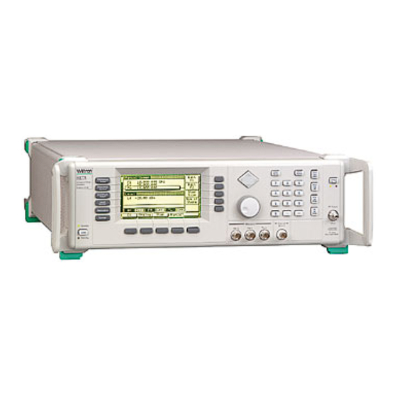
- Page 12 Figure 1-1. Typical Series 680XXB/681XXB Synthesized CW/Sweep Generator (Model 68169B Shown)
-
Page 13: Scope Of Manual
Chapter 1 General Information SCOPE OF MANUAL This manual provides service information for all models of the Series 680XXB Synthesized CW Generator and the Series 681XXB Synthe- sized Sweep Generator. The service information includes replaceable parts information, functional circuit descriptions, block diagrams, per- formance verification tests, and procedures for calibration, trouble- shooting, and assembly/subassembly removal and replacement. - Page 14 GENERAL 680XXB/681XXB INFORMATION MODELS Table 1-1. Series 680XXB/681XXB Models (1 of 2) 68XXXB Frequency Output Power Output Power Model (GHz) w/Step Attenuator 68X37B 2.0 – 20.0 GHz +13.0 dBm +11.0 dBm 68X45B 0.5 – 20.0 GHz +13.0 dBm +11.0 dBm 68X47B 0.01 –...
- Page 15 GENERAL 680XXB/681XXB INFORMATION MODELS Table 1-1. Series 680XXB/681XXB Models (2 of 2) 68XXXB Frequency Output Power Output Power Model (GHz) w/Step Attenuator 0.01 – 2.0 GHz +12.0 dBm 2.0 – 20.0 GHz +10.0 dBm 68X97B 20.0 – 40.0 GHz +2.5 dBm Not Available 40.0 –...
-
Page 16: Identification Number
INFORMATION NUMBER IDENTIFICATION NUMBER All ANRITSU instruments are assigned a unique six-digit ID number, such as “403002”. The ID number is imprinted on a decal that is af- fixed to the rear panel of the unit. Special-order instrument configura- tions also have an additional special serial number tag attached to the rear panel of the unit. -
Page 17: Options
Option 11, 0.1 Hz Frequency Resolution. Provides frequency resolution of 0.1 Hz. Option 14, ANRITSU 360B VNA Compatibility. Modifies rack mounting hardware to mate unit in a ANRITSU 360B VNA con- sole. Option 15A, High Power Output. Adds high-power RF compo- nents to the instrument in the 2–26.5 GHz frequency range. -
Page 18: Level Of Maintenance
GENERAL LEVEL OF INFORMATION MAINTENANCE Options 17A & 17B, No Front Panel. Deletes the front panel for use in remote control applications where a front panel display or keyboard control are not needed. Option 17A deletes the front panel from 681XXB models; Option 17B deletes the front panel from 680XXB models. - Page 19 GENERAL PREVENTIVE INFORMATION MAINTENANCE PREVENTIVE The 680XXB/681XXB must always receive adequate ventilation. A blocked fan filter can cause the instrument to overheat and shut down. MAINTENANCE Check and clean the rear panel fan honeycomb filter periodically. Clean the fan honeycomb filter more frequently in dusty environ- ments.
-
Page 20: Static-Sensitive Component Handling Precautions
GENERAL STATIC-SENSITIVE COMPONENT INFORMATION HANDLING PRECAUTIONS 1. Do not touch exposed contacts 2. Do not slide static sensitive 3. Do not handle static sensitive on any static sensitive component across any surface. components in areas where the component. floor or work surface covering is capable of generating a static charge. -
Page 21: Startup Configurations
GENERAL START UP INFORMATION CONFIGURATION 1-11 STARTUP The 680XXB/681XXB comes from the factory with a jumper across CONFIGURATIONS pins 2 and 3 of front panel connector J12 (Figure 1-4). In this configu- ration, connecting the instrument to line power automatically places it in operate mode (front panel OPERATE LED on). -
Page 22: Recommended Test Equipment
Power Sensor (1mW to 100mW) Power Sensor: HP 8487A (0.01 to 50 GHz) Power Meter, Power Range: –30 to +20 dBm ANRITSU ML4803A, with with Power Sensor (1mW to 100mW) Power Sensor: MP716A4 (50 to 75 GHz) Digital Multimeter Resolution: 4-1/2 digits (to 20V) John Fluke, Inc., Model 8840A, with... - Page 23 Mixer Frequency Range: 1 to 26 GHz Macom Micro Electronics Div. Model DMS1-26A Scalar Network Frequency Range: 0.01 to 50 GHz ANRITSU, Model 562, with C, T Analyzer, with RF Detector: RF Detector 560-7K50 (0.01 to 40 GHz) 560-7VA50 (0.01 to 50 GHz)
-
Page 24: Exchange Assembly Program
For more information about the program, contact your local sales rep- resentative or call your local ANRITSU service center. Refer to Table 1-5, on page 1-19, for a list of current ANRITSU service centers. 1-14 680XXB/681XXB MM... -
Page 25: Replaceable Subassemblies And Parts
PARTS LIST 1-14 REPLACEABLE Table 1-3 lists those replaceable subassemblies and RF components of the 680XXB/681XXB that are presently covered by the ANRITSU ex- SUBASSEMBLIES AND PARTS change assembly program. Table 1-4, on page 1-17, lists common re- placeable parts for the 680XXB/681XXB that are not presently on the exchange assembly program. - Page 26 INFORMATION PARTS LIST Table 1-3. Replaceable Subassemblies and RF Components (2 of 3) SUBASSEMBLY OR PART NAME ANRITSU PART NUMBER Printed Circuit Board Assemblies (Continued) A14 SDM Driver PCB Assy 40 GHz D37434-3 A14 SDM Driver PCB Assy 26.5 GHz...
- Page 27 GENERAL INFORMATION PARTS LIST Table 1-3. Replaceable Subassemblies and RF Components (3 of 3) SUBASSEMBLY OR PART NAME ANRITSU PART NUMBER Switched Filter D29393 RF Components (Continued) Switched Filter (w/Option 15A) D26340 Switched Filter (w/Option 15A) ND39376 Switched Filter (w/Option 15A)
- Page 28 GENERAL INFORMATION PARTS LIST Table 1-4. Common Replaceable Subassemblies and Parts (2of 2) SUBASSEMBLY OR PART NAME ANRITSU PART NUMBER Handle, Side Carrying 783-830 Screw, Handle Side Carrying 900-714 Line Module 260-11 Shield, High Voltage Line Filter B37061 Shield Cover...
- Page 29 GENERAL ANRITSU INFORMATION SERVICE CENTERS Table 1-5. ANRITSU Service Centers UNITED STATES FRANCE JAPAN ANRITSU COMPANY ANRITSU S.A ANRITSU CUSTOMER SERVICE LTD. 490 Jarvis Drive 9 Avenue du Quebec 1800 Onna Atsugi-shi Morgan Hill, CA 95037-2809 Zone de Courtaboeuf Kanagawa-Prf. 243 Japan...
- Page 31 Chapter 2 Functional Description Table of Contents INTRODUCTION ....2-3 680XXB/681XXB MAJOR SUBSYSTEMS ..2-3 Digital Control....2-4 Front Panel .
- Page 32 Table Of Contents (Continued) Switched Doubler Module ... . 2-30 Source Quadrupler Module ... 2-33 Power Level Detection/ALC Loop ..2-35 Step Attenuator .
-
Page 33: Introduction
Chapter 2 Functional Description INTRODUCTION This chapter provides brief functional descriptions of the major sub- systems that are contained in each model of the Series 680XXB/ 681XXB Synthesized CW/Sweep Generators. In addition, the opera- tion of the frequency synthesis, automatic level control (ALC), and RF deck subsystems is described so that the reader may better under- stand the overall operation of the instrument. -
Page 34: Digital Control
FUNCTIONAL 680XXB/681XXB DESCRIPTION MAJOR SUBSYSTEMS Digital This circuit subsystem consists of the A17 CPU and Control A16 CPU Interface PCBs. The central processor unit (CPU) is the main controller for the 680XXB/ 681XXB. This controller directly or indirectly con- trols all functions of the instrument. The CPU con- tains memory that stores the main operating system components and instrument firmware, instrument calibration data, and front panel setups in the... -
Page 35: Analog Instruction
FUNCTIONAL 680XXB/681XXB DESCRIPTION MAJOR SUBSYSTEMS The A3 Reference Loop PCB supplies the sta- ble 10 MHz and 500 MHz reference frequency signals for the rest of the frequency synthesis system. The A4 Coarse Loop PCB generates coarse tuning frequencies of 439 to 490 MHz (219.5 to 245 MHz for 680XXB/681XXB models with se- rial number 512001 and above) for use by the YIG Loop. - Page 36 FUNCTIONAL 680XXB/681XXB DESCRIPTION MAJOR SUBSYSTEMS Front Panel Rear Panel Connectors Inputs Outputs Power Input ∗ To A11 AM/FM PCB To A3 AM IN 10 MHz REF IN (Via A20 Motherboard) Reference Loop ∗ To A11 AM/FM PCB From RF Deck FM IN RF OUTPUT (Via A20 Motherboard)
- Page 37 FUNCTIONAL 680XXB/681XXB DESCRIPTION MAJOR SUBSYSTEMS Serial Data Serial Data Serial Data 10 MHz REF OUT 10 MHz Rear Panel BNC 10 MHz Reference Coarse Fine 500 MHz Loop Loop Loop 439 - 440 MHz 500 MHz Frequency 10 MHz REF IN Synthesis Rear Panel BNC 21.5 - 40 MHz...
- Page 38 FUNCTIONAL 680XXB/681XXB DESCRIPTION MAJOR SUBSYSTEMS Front Panel Rear Panel Connectors Inputs Outputs Power Input ∗ To A10 ALC PCB To A3 AM IN 10 MHz REF IN (Via A20 Motherboard) Reference Loop ∗ To A11 FM PCB From RF Deck FM IN RF OUTPUT (Option 9)
- Page 39 FUNCTIONAL 680XXB/681XXB DESCRIPTION MAJOR SUBSYSTEMS Serial Data Serial Data Serial Data 10 MHz REF OUT Real Panel BNC 10 MHz 10 MHz 10 MHz (To A6) 500 MHz Reference Coarse Fine Loop Loop Loop 500 MHz 219.5 - 245 MHz (To Down Converter) 10 MHz REF IN...
-
Page 40: Yig Driver
FUNCTIONAL 680XXB/681XXB DESCRIPTION MAJOR SUBSYSTEMS YIG Driver The A13 YIG Driver PCB supplies the tuning cur- rent and bias voltages for the 2 to 20 GHz YIG- tuned oscillator. It also provides bias voltages for the Down Converter assembly and the amplifiers located in the Switched Filter assembly. -
Page 41: Power Supply
FUNCTIONAL 680XXB/681XXB DESCRIPTION MAJOR SUBSYSTEMS rupler Module (SQM), the Directional Coupler/Level Detector, and the optional 110 dB (90 dB) Step Attenuator. Refer to paragraph 2-5 for a functional overview of the RF deck subsystem. Power Supply The power supply subsystem consists of the A15 Regulator PCB, the A18 Power Supply PCB, the A19 Line Conditioner PCB, and part of the A21 Rear Panel PCB and Rear Casting Assembly. -
Page 42: Motherboard/Interconnections
FUNCTIONAL FREQUENCY DESCRIPTION SYNTHESIS Motherboard/ The A20 Motherboard PCB and associated cables Interconnec- provide the interconnections for the flow of data, tions signals, and DC voltages between all internal com- ponents and assemblies throughout the 680XXB/ 681XXB. FREQUENCY SYNTHESIS The frequency synthesis subsystem provides phase-lock control of the 680XXB/681XXB output frequency. - Page 43 FUNCTIONAL FREQUENCY DESCRIPTION SYNTHESIS A5 Fine Loop 10 MHz Phase A3 Reference Loop A4 Coarse Loop Error 10 MHz 206 - 391 MHz Frequency ÷ 10 ÷ 100 10 MHz REF In Synthesizer Phase/ 10 MHz 1 MHz 100 kHz ÷...
- Page 44 FUNCTIONAL FREQUENCY DESCRIPTION SYNTHESIS A4 Coarse Loop A5 Fine Loop 10 MHz 10 MHz Phase A3 Reference Loop Error Frequency 206 - 391 MHz ÷ 10 ÷ 100 10 MHz REF In Synthesizer Phase/ 10 MHz 10 MHz 1 MHz 100 kHz ÷...
-
Page 45: Overall Operation
FUNCTIONAL FREQUENCY DESCRIPTION SYNTHESIS In the A3 Reference Loop, the 100 MHz VCXO can be controlled by the phase-lock loop using a 10 MHz reference. This is because a divide-by-ten circuit is between the VCXO's output and the variable input to the phase-lock loop. - Page 46 FUNCTIONAL FREQUENCY DESCRIPTION SYNTHESIS Table 2-1. RF Output and Loop Frequencies cuitry and the FM coil drivers) to eliminate any fre- (680XXB/681XXB Models prior to Serial Num- quency difference between the two signals. ber 512001) Phase locking the instrument's output frequency RF OUTPUT/LOOP FREQUENCIES over a broad frequency range is accomplished by (in MHz)
-
Page 47: Rf Outputs 0.01 To 65 Ghz
FUNCTIONAL FREQUENCY DESCRIPTION SYNTHESIS RF Outputs Refer to the block diagram of the RF Deck shown in 0.01 to 65 GHz Figure 2-2 (page 2-9) for the following description. The 680XXB/681XXB uses one 2 to 20 GHz YIG- tuned oscillator. All other frequencies output by the instrument are derived from the fundamental fre- quencies generated by this YIG-tuned oscillator. -
Page 48: Frequency Modulation (681Xxb Only)
FUNCTIONAL FREQUENCY DESCRIPTION SYNTHESIS Frequency Frequency modulation (FM) of the YIG-tuned oscil- Modulation lator RF output by external signals is performed by (681XXB only) summing the external modulating signal into the FM control path of the YIG loop. Refer to Figures 2-1, 2-2, 2-3, and 2-4. -
Page 49: Alc And Modulation
FUNCTIONAL ALC AND DESCRIPTION MODULATION ALC AND MODULATION The ALC and modulation subsystem provides automatic level control (ALC), and in the 681XXB, amplitude modulation (AM) and square wave modulation of the RF output signal. The ALC loop consists of cir- cuits located on the A10 ALC PCB, the A9 PIN Control PCB, and the A14 SDM, SQM Driver PCB. -
Page 50: Amplitude Modulation (681Xxb Only)
FUNCTIONAL ALC AND DESCRIPTION MODULATION The Level Reference DAC, under the control of the CPU, provides the RF level reference voltage. By setting the output of this DAC to the appropriate voltage, the CPU adjusts the RF output power to the level selected by the user. - Page 51 FUNCTIONAL ALC AND DESCRIPTION MODULATION Figure 2-5. Block Diagram of the ALC and Modulation Subsystem (680XXB/681XXB Prior to Serial Number 512001) 680XXB/681XXB 2-21...
- Page 52 FUNCTIONAL ALC AND DESCRIPTION MODULATION Figure 2-6. Block Diagram of the ALC and Modulation Subsystem (680XXB/681XXB Se- rial Number 512001 and Above) 680XXB/681XXB 2-22...
-
Page 53: Square Wave Modulation (681Xxb Only)
FUNCTIONAL ALC AND DESCRIPTION MODULATION log. After processing, the modulating signals go to the A10 PCB. On the A10 PCB, the AM Calibration DAC, under control of the CPU, adjusts the modu- lating signals for the proper amount of AM. The ad- justed modulating signal is then summed with the level reference, slope, and detector inputs into the ALC loop. - Page 54 FUNCTIONAL RF DECK DESCRIPTION ASSEMBLIES RF DECK ASSEMBLIES The primary purpose of the RF deck assembly is to generate CW and swept frequency RF signals and route these signals to the front panel RF OUTPUT connector. It is capable of generating RF signals in the frequency range of 0.01 to 65 GHz.
- Page 55 FUNCTIONAL RF DECK DESCRIPTION ASSEMBLIES RF Path for 20 GHz Models Switched Doubler Module - ND40843 20 - 26.5 GHz (26.5 GHz Models) >+8.5 dBm 20 - 26.5 GHz BPF Bias Switch Control 20 - 40 GHz Switched Doubler Module - D28535 >+8.5 dBm Switched Filter Assy.
- Page 56 FUNCTIONAL RF DECK DESCRIPTION ASSEMBLIES À S o u r c e Q u a d r u p l e r M o d u l e  1 6 . 8 G H z L P F B P F &...
-
Page 57: Rf Deck Assemblies
FUNCTIONAL RF DECK DESCRIPTION ASSEMBLIES YIG-tuned The 2 to 20 GHz YIG-tuned oscillator actually con- Oscillator tains two oscillators—one covering the frequency range of 2 to 8.4 GHz and one covering the fre- quency range of 8.4 to 20 GHz. Both oscillators use a common internal amplifier. -
Page 58: Rf Signal Filtering
FUNCTIONAL RF DECK DESCRIPTION ASSEMBLIES The modulator control signal is received from the A9 PIN Control PCB where it is developed from the ALC control signal. The modulator control signal adjusts the gain of the modulator to control the power level of the RF output signals. In the 681XXB, the modulator is also used for AM and square wave modulation of the RF output signals. -
Page 59: To 2 Ghz Down Converter
FUNCTIONAL RF DECK DESCRIPTION ASSEMBLIES From J2, the RF signal goes to either the directional coupler (£20 GHz models) or the input connector J1 on the switched doubler module (>20 GHz models). 0.01 to 2 GHz The 0.01 to 2 GHz Down Converter assembly (Fig- Down ures 2-7 and 2-8) contains a 6.5 GHz VCO that is Converter... -
Page 60: Switched Doubler Module
FUNCTIONAL RF DECK DESCRIPTION ASSEMBLIES quency dividers, the 0.5 to 2.2 GHz RF signal then goes to the modulator which provides power level control. The modulator control signal is received from the from the A9 PIN Control PCB where it is developed from the ALC control signal. - Page 61 FUNCTIONAL RF DECK DESCRIPTION ASSEMBLIES RF Path for 20 GHz Models Switched Doubler Module - ND40843 20 - 26.5 GHz (26.5 GHz Models) >+8.5 dBm 20 - 26.5 GHz BPF Bias Switch Control 20 - 40 GHz >+8.5 dBm Switched Doubler Module - D28535 Switched Filter Assy.
- Page 62 FUNCTIONAL RF DECK DESCRIPTION ASSEMBLIES À S o u r c e Q u a d r u p l e r M o d u l e  1 6 . 8 G H z L P F B P F &...
-
Page 63: Source Quadrupler Module
FUNCTIONAL RF DECK DESCRIPTION ASSEMBLIES the A14 SDM.SQM Driver PCB. The RF signal is amplified, then doubled in frequency. From the dou- bler, the 20 to 26.5 GHz RF signal goes to the band- pass filter. After passing through the bandpass filter, the 20 to 26.5 GHz RF signal is multiplexed by the PIN switches to the SDM output at connector J2. - Page 64 FUNCTIONAL RF DECK DESCRIPTION ASSEMBLIES modulator, the 40 to 50 GHz RF signals goes via a band-pass filter to output connector J3 of the for- ward coupler. Note that on the 40 to 50 GHz SQM (P/N D28185), the forward coupler is an integral part of the SQM.
-
Page 65: Power Level Detection/Alc Loop
FUNCTIONAL RF DECK DESCRIPTION ASSEMBLIES Power Level The RF output signal from either the switched filter Detection/ assembly (£20 GHz models), the SDM (£26.5 GHz or £40 GHz models), or forward coupler (>40 GHz mod- ALC Loop els) goes to the directional coupler for transfer to the RF OUTPUT connector. - Page 67 Chapter 3 Performance Verification Table of Contents INTRODUCTION ....3-3 RECOMMENDED TEST EQUIPMENT ..3-3 TEST RECORDS ....3-3 CONNECTOR AND KEY LABEL NOTATION .
- Page 68 Table of Contents (Continued) 3-11 POWER LEVEL ACCURACY AND FLATNESS TESTS ......3-26 Test Setup ....3-26 Power Level Accuracy Test Procedure .
-
Page 69: Introduction
In some cases, the user may substitute test equipment hav- ing the same critical specifications as those on the recommended test equipment list. Contact your local ANRITSU service center (refer to Table 1-5 on page 1-18) if you need clarification of any equipment or procedural refer- ence. - Page 70 (1mW to 100mW) Power Sensor: Power Sensor HP 8487A (0.01 to 50 GHz) Power Meter Power Range: –30 to +20 dBm ANRITSU ML4803A, with 3-11 with (1mW to 100mW) Power Sensor: Power Sensor MP716A4 (50 to 75 GHz) Frequency Reference Frequency: 10 MHz Absolute Time Corp., Model 300...
- Page 71 TEST INSTRUMENT SPECIFICATION MANUFACTURER/MODEL NUMBER Attenuator Frequency Range: DC to 40 GHz ANRITSU, Model 41KC-20 Max Input Power: >+17 dBm Attenuation: 20 dB Attenuator Frequency Range: DC to 60 GHz ANRITSU, Model 41V-10 3-9, 3-10 Max Input Power: >+17 dBm...
-
Page 72: 680Xxb/681Xxb Power Levels
PERFORMANCE 680XXB/681XXB VERIFICATION POWER LEVELS 680XXB/681XXB POWER Table 3-2 is a listing of the Series 680XXB and 681XXB Synthesized CW/Sweep Generator models and their maximum leveled ouput power LEVELS levels. Certain test procedures will refer you to this table for the maxi- mum leveled output power level setting of the instrument model being tested. - Page 73 PERFORMANCE 680XXB/681XXB VERIFICATION POWER LEVELS Table 3-2. 680XXB/681XXB Maximum Leveled Output Power (2 of 2) Max Leveled 68XXXB Frequency Max Leveled Output Power Model (GHz) Output Power w/Step Attenuator 0.5 – 2.2 GHz +11.0 dBm 2.2 – 20.0 GHz +10.0 dBm 68X95B 20.0 –...
-
Page 74: Internal Time Base Aging Rate Test
PERFORMANCE INTERNAL TIME BASE VERIFICATION AGING RATE TEST INTERNAL TIME BASE The following test can be used to verify that the 680XXB/681XXB 10 MHz time base is within its aging specification. The instrument AGING RATE TEST (Optional) derives its frequency accuracy from an internal 100 MHz crystal oscil- lator standard. -
Page 75: Test Procedure
PERFORMANCE INTERNAL TIME BASE VERIFICATION AGING RATE TEST Test The frequency error is measured at the start and Procedure finish of the test time period of 24 hours. The aging rate is the difference between the two error read- ings. 1. - Page 76 PERFORMANCE INTERNAL TIME BASE VERIFICATION AGING RATE TEST 4. Record the frequency error value, displayed on the Frequency Reference, on the Test Record. 5. Wait for 24 hours, then record the current fre- quency error value on the Test Record. 6.
-
Page 77: Frequency Synthesis Tests
PERFORMANCE FREQUENCY VERIFICATION SYNTHESIS TESTS FREQUENCY SYNTHESIS The following tests can be used to verify correct operation of the fre- quency synthesis circuits. Frequency synthesis testing is divided into TESTS two parts—coarse loop/YIG loop tests and fine loop tests. 680XXB / 681XXB FREQUENCY COUNTER Band 3 Band 4... -
Page 78: Coarse Loop/Yig Loop Test Procedure
PERFORMANCE FREQUENCY VERIFICATION SYNTHESIS TESTS e. For measuring frequencies of 60.0 to 65.0 GHz, connect to the Band 4 input via the Option 93 waveguide mixer (Connection B). Coarse Loop/ The following procedure tests both the coarse loop YIG Loop Test and YIG loop by stepping the instrument through Procedure its full frequency range in 1 GHz steps and measur-... -
Page 79: Fine Loop Test Procedure
PERFORMANCE FREQUENCY VERIFICATION SYNTHESIS TESTS Fine Loop The following procedure tests the fine loop by step- Test ping the instrument through ten 1 kHz steps (ten Procedure 100 Hz steps for instruments with Option 11) and measuring the RF output at each step. 1. -
Page 80: Spurious Signals Test: Rf Output Signals £2 Ghz (£2.2 Ghz For 68Xx5B Models)
PERFORMANCE SPURIOUS SIGNALS TEST: RF OUTPUT SIGNALS £2 GHz (£2.2 GHz for 68XX5B MODELS) VERIFICATION SPURIOUS SIGNALS The following test can be used to verify that the CW/sweep generator meets it spurious signal specifications for RF output signals from 0.01 TEST: RF OUTPUT SIGNALS £2 GHz to 2 GHz (0.5 to 2.2 GHz for 68XX5B models). - Page 81 PERFORMANCE SPURIOUS SIGNALS TEST: RF OUTPUT SIGNALS £2 GHz (£2.2 GHz for 68XX5B MODELS) VERIFICATION 2. Set up the 680XXB/681XXB as follows: a. Reset the instrument by pressing SYSTEM then Reset . Upon reset the CW Menu is dis- played. b.
- Page 82 PERFORMANCE SPURIOUS SIGNALS TEST: RF OUTPUT SIGNALS £2 GHz (£2.2 GHz for 68XX5B MODELS) VERIFICATION presence by entering their levels on the Test Re- cord. 9. Set F1 to 1.6 GHz. Measure the worst case non- harmonic signal for the 1.6 GHz carrier and rec- ord its presence by entering its level on the Test Record.
-
Page 83: 2.2 Ghz Test Procedure
PERFORMANCE SPURIOUS SIGNALS TEST: RF OUTPUT SIGNALS £2 GHz (£2.2 GHz for 68XX5B MODELS) VERIFICATION 0.5 - 2.2 GHz The following procedure lets you measure the 0.5 to Test 2.2 GHz RF output harmonic levels to verify that Procedure they meet specifications. 1. - Page 84 PERFORMANCE HARMONIC TEST: RF OUTPUT VERIFICATION SIGNALS FROM 2 TO 20 GHz HARMONIC TEST: RF The following test can be used to verify that the 680XXB/681XXB meets its harmonic specifications for RF output signals from 2 to OUTPUT SIGNALS FROM 2 TO 20 GHz 20 GHz (2.2 to 20 GHz for 68XX5B Models).
-
Page 85: Harmonic Test: Rf Output Signals From 2 To 20 Ghz
PERFORMANCE HARMONIC TEST: RF OUTPUT VERIFICATION SIGNALS FROM 2 TO 20 GHz Test The following procedure lets you measure the 2 to Procedure 10 GHz (2.2 to 10 GHz for 68XX5Bs) RF output har- (2 to 10 GHz) monic levels to verify that they meet specifications. 1. -
Page 86: Test Procedure (11 To 20 Ghz)
PERFORMANCE HARMONIC TEST: RF OUTPUT VERIFICATION SIGNALS FROM 2 TO 20 GHz Test The following procedure lets you measure the 11 to Procedure 20 GHz RF output harmonic levels to verify that (11 to 20 GHz) they meet specifications. NOTE Because an external mixer is required for these measurements, the RF output flat- ness of the 680XXB/681XXB instrument is... - Page 87 PERFORMANCE HARMONIC TEST: RF OUTPUT VERIFICATION SIGNALS FROM 2 TO 20 GHz 4. Remove Connection A and connect the 680XXB/ 681XXB RF OUTPUT to the waveguide mixer in- put of the Spectrum Analyzer as shown in Con- nection B. 5. On the 680XXB/681XXB, remove 30 dB of at- tenuation from the RF output.
-
Page 88: Single Sideband Phase Noise Test
PERFORMANCE SINGLE SIDEBAND VERIFICATION PHASE NOISE TEST 3-10 SINGLE SIDEBAND The following test can be used to verify that the 680XXB/681XXB meets its single sideband phase noise specifications. For this test, a PHASE NOISE TEST second 680XXB/681XXB is required. This additional instrument acts as a local oscillator (LO). -
Page 89: Test Procedure
PERFORMANCE SINGLE SIDEBAND VERIFICATION PHASE NOISE TEST Test The following procedure lets you measure the RF Procedure output single sideband phase noise levels to verify that they meet specifications. NOTE The following technique is a measurement of phase noise and AM noise. To avoid erro- neous results, on the 680XXB/681XXB DUT set L1 for maximum leveled output power and select External Detector level-... - Page 90 PERFORMANCE SINGLE SIDEBAND VERIFICATION PHASE NOISE TEST 3. Set up the Spectrum Analyzer as follows: Table 3-7. Single Sideband Phase Noise a. Center Frequency: 1 MHz Test Specification b. Frequency Span: 300 Hz CW Carrier Offset From Test Frequency Carrier Specification* c.
- Page 91 PERFORMANCE SINGLE SIDEBAND VERIFICATION PHASE NOISE TEST 9. On the Spectrum Analyzer: a. Deselect NOISE LVL. b. Set Frequency Span to 300 kHz. c. Adjust the Marker for a 100 kHz offset. d. Select NOISE LVL. 10. Measure the phase noise level 100 kHz offset from the carrier frequency.
-
Page 92: Power Level Accuracy And Flatness Tests
PERFORMANCE POWER LEVEL ACCURACY VERIFICATION AND FLATNESS TESTS 3-11 POWER LEVEL The following tests can be used to verify that the 680XXB/681XXB meets its power level specifications. Power level verification testing is ACCURACY AND FLATNESS TESTS divided into two parts—power level accuracy tests and power level flatness tests. -
Page 93: Power Level Accuracy Test Procedure
PERFORMANCE POWER LEVEL ACCURACY VERIFICATION AND FLATNESS TESTS Power Level Power level accuracy is tested by stepping the out- Accuracy Test put power level down in 1 dB increments from its Procedure maximum rated power level and measuring the out- put power level at each step. - Page 94 PERFORMANCE POWER LEVEL ACCURACY VERIFICATION AND FLATNESS TESTS c. With the Step Sweep Menu displayed, press the main menu key FREQUENCY CONTROL The Sweep Frequency Control Menu is then displayed. d. Press Full to select a full range frequency sweep. e.
- Page 95 PERFORMANCE POWER LEVEL ACCURACY VERIFICATION AND FLATNESS TESTS 3. Set up the 681XXB as follows for an analog sweep power level flatness test: a. Reset the instrument by pressing SYSTEM then Reset . The CW Menu is displayed. b. Press Analog to place the 681XXB in the ana- log sweep frequency mode and display the Analog Sweep Menu.
- Page 97 Chapter 4 Calibration Table of Contents INTRODUCTION ....4-3 RECOMMENDED TEST EQUIPMENT ..4-3 TEST RECORDS ....4-3 CALIBRATION FOLLOWING SUBASSEMBLY REPLACEMENT.
- Page 98 Table of Contents (Continued) 4-11 ALC BANDWIDTH CALIBRATION ..4-31 Equipment Setup ....4-31 Bandwidth Calibration ... . . 4-31 4-12 AM CALIBRATION (681XXB Only) Firmware Versions 2.17 to 3.00 .
-
Page 99: Introduction
In some cases, the user may substitute test equipment having the same critical specifications as those on the recommended test equipment list. Contact your local ANRITSU service center (Refer to Table 1-5 on page 1-18) if you need clarification of any equipment or procedural reference. -
Page 100: Calibration Following Subassembly Replacement
(1mW to 100 mW) Power Sensor: Power Sensor HP 8487A (0.01 to 50 GHz) Power Meter Power Range: –30 to +20 dBm ANRITSU ML4803A, with 4-12 with (1mW to 100mW) Power Sensor: Power Sensor MP716A4 (50 to 75 GHz) - Page 101 AM Depth: 0% to 90% AM Modulation Rates: DC to 100 kHz Filters: 20 kHz lowpass, 300 Hz highpass Scalar Network Frequency Range: 0.01 to 50 GHz ANRITSU Model 562, with 4-8, 4-10 Analyzer, with RF Detector: RF Detector 560-7K50 (0.01 to 40 GHz) 560-7VA50 (0.01 to 50 GHz)
- Page 102 CALIBRATION FOLLOWING CALIBRATION SUBASSEMBLY REPLACEMENT Table 4-2. Calibration Following Subassembly/RF Component Replacement Perform the Following Subassembly/RF Component Replaced Calibration(s) in Paragraph(s): A1, A2 Front Panel Assy None A3 Reference Loop PCB A4 Coarse Loop PCB A5 Fine Loop PCB A6 Square Wave Generator PCB None A7 YIG Loop PCB None...
-
Page 103: Initial Setup
680XXB / 681XXB IBM-Compatible PC Figure 4-1. PC to 680XXB/681XXB Interconnection for Calibration Interconnec- Using the ANRITSU P/N T1678 serial interface as- tion sembly, connect the PC to the 680XXB/681XXB as follows: 1. Connect the wide flat cable between the 680XXB/ 681XXB rear panel SERIAL I/O connector and the P1 connector on the T1678 serial interface PCB. -
Page 104: Pc Setup - Windows 3.1
CALIBRATION INITIAL SETUP PC Setup — Configure the PC with Windows 3.1 operating sys- Windows 3.1 tem to interface with the 680XXB/681XXB as fol- lows: 1. Power up the 680XXB/681XXB. 2. Power up the PC and place in Windows. 3. Double click on the Terminal Icon to bring up the Terminal (Untitled) window. - Page 105 CALIBRATION INITIAL SETUP 5. Click on Communications. 6. At the Communications Dialog box, select the fol- lowing options: NOTE Baud Rate 9600 (See Note) When calibrating instruments with Data Bits operating firmware Version 3.03 Stop Bits and above (Version 1.00 and above Parity None for 680X5B/681X5B models), set the...
-
Page 106: Pc Setup - Windows 95
CALIBRATION INITIAL SETUP 7. After making the selections, click on the OK but- ton. 8. Press <ENTER> on the keyboard. 9. Verify that a prompt appears on the PC display. 10. This completes the initial setup for calibration. PC Setup — Configure the PC with Windows 95 operating sys- Windows 95 tem to interface with the 680XXB/681XXB as fol-... - Page 107 CALIBRATION INITIAL SETUP 7. In the New Connection Name box, type a name for the connection, then click on the OK button. The window below is now displayed. Direct to 8. In the Connect using box, type: Com “_” . Enter the number of the communica- tions port being used, for example: Com 1.
- Page 108 CALIBRATION INITIAL SETUP 10. In the Properties window, make the following se- lections: NOTE Bits per second 19200 (See Note) When calibrating instruments with Data bits operating firmware below Version Parity None 2.00, set the Bits per second rate to Stop bits 9600.
-
Page 109: Preliminary Calibration
PRELIMINARY CALIBRATION CALIBRATION PRELIMINARY This procedure provides the steps necessary to initially calibrate the coarse loop, fine loop, frequency instruction, and internal DVM cir- CALIBRATION cuitry and the 100 MHz reference oscillator of the 680XXB/681XXB. Figure 4-2. Equipment Setup for Preliminary Calibration Equipment Connect the equipment, shown in Figure 4-2, as fol- Setup... -
Page 110: Calibration Steps
PRELIMINARY CALIBRATION CALIBRATION Calibration Each of the steps in this procedure provides initial Steps calibration of a specific 680XXB/681XXB circuit or component. To ensure accurate instrument calibra- tion, each step of this procedure must be performed in sequence. 1. Calibrate the internal DVM circuitry as follows: calterm 119 a. - Page 111 PRELIMINARY CALIBRATION CALIBRATION 6. Calibrate the YIG Frequency Linearizer DACs as follows: calterm 127 a. At the prompt, type: press <ENTER>. b. Follow the instructions on the screen. Enter the value of the frequency counter reading as XXXX MHz. c Record step completion on the Test Record. 7.
- Page 112 PRELIMINARY CALIBRATION CALIBRATION 10. Calibrate the Sweep Width DAC as follows: calterm 133 a. At the prompt, type: press <ENTER>. (This calibration can take ap- proximately 2 minutes to complete.) prompt will appear on the screen when the calibration is complete. b.
-
Page 113: Switched Filter Shaper Calibration
SWITCHED FILTER CALIBRATION SHAPER CALIBRATION SWITCHED FILTER This procedure provides the steps necessary to adjust the Switched SHAPER CALIBRATION Filter Shaper Amplifier gain to produce a more constant level ampli- fier gain with power level changes. 562 Network Analyzer 680XXB / 681XXB IBM-Compatible PC Serial GPIB... -
Page 114: Log Amplifier Zero Calibration
SWITCHED FILTER CALIBRATION SHAPER CALIBRATION Log Amplifier Before the Switched Filter Shaper Amplifier can be Zero Calibra- adjusted, zero calibration of the ALC Log amplifier tion must performed to eliminate any DC offsets. 1. Perform ALC Log amplifier zero calibration as follows: a. -
Page 115: Shaper Dac Adjustment
SWITCHED FILTER CALIBRATION SHAPER CALIBRATION 2. Adjust the Switched Filter Limiter DAC for each of the frequency bands as follows: a. At the prompt on the PC display, type: calterm 145 and press <ENTER>. b. On the 562 Network Analyzer, set the Resolu- Shaper Amplifier tion to 0.2 dB and adjust the offset to center... - Page 116 SWITCHED FILTER CALIBRATION SHAPER CALIBRATION c. Press CHANNEL 2 DISPLAY: OFF. d. Press CHANNEL 1 DISPLAY: ON. e. Press CHANNEL 1 MENU key. f. From the Channel 1 Menu display, select POWER. g. Press OFFSET/RESOLUTION. b. Set Resolution to 5 dB/Div. c.
- Page 117 SWITCHED FILTER CALIBRATION SHAPER CALIBRATION Shaper DAC For Models 680XXB with Firmware Version Adjustment 3.37 and above; Models 681XXB with Firmware Version 3.42 and above; Models 680X5B with Firmware Version 1.24 and above; and Models 681X5B with Firmware Version 1.30 and above. The following step in the procedure adjusts the Switch Filter Shaper DAC which controls the gain of the Switched Filter Shaper Amplifier.
-
Page 118: Rf Level Calibration
Switched Doubler Module (SDM), the Source Quadrupler Module (SQM), the Forward Coupler, the Directional Coupler, or the Step Attenuator. The RF level calibration software is available from ANRITSU by or- dering: Part number 2300-104, Version 2.0 and above, for all £50 GHz 680XXB/681XXB models. -
Page 119: Alc Slope Calibration
ALC SLOPE CALIBRATION CALIBRATION 4-10 ALC SLOPE Models 681XXB with Firmware Versions 2.17 to 3.00 CALIBRATION This procedure provides the steps necessary to perform ALC Slope calibration. The ALC Slope DAC is calibrated to adjust for an increas- ing or decreasing output power-vs-output frequency in the analog sweep mode. -
Page 120: Alc Slope Dac Adjustment
ALC SLOPE CALIBRATION CALIBRATION NOTE Before beginning this calibration proce- dure, always let the 681XXB warm up for a minimum of one hour. ALC Slope The following procedure lets you adjust the ALC Slope DAC to compensate for decreasing output power-vs-frequency for frequencies £2 GHz and for Adjustment frequencies ³2 GHz. - Page 121 ALC SLOPE CALIBRATION CALIBRATION 3. Make the following selections on the 562 Network Analyzer to normalize the step sweep. a. Press CALIBRATION and follow the menu on the display. b. Press AUTOSCALE. c. Press OFFSET/RESOLUTION and set the Resolution to 0.2 dB. 4.
- Page 122 ALC SLOPE CALIBRATION CALIBRATION f. Press Sweep Ramp . At the resulting Step Sweep Ramp Menu, press Num of Steps and set the number of steps to 200. g. Press Step to return to the Step Sweep Menu display. 7. Make the following selections on the 562 Network Analyzer to normalize the step sweep.
-
Page 123: Firmware Version 3.03 And Above
ALC SLOPE CALIBRATION CALIBRATION Models 681XXB with Firmware Version 3.03 and above (Models 681X5B with Firmware Version 1.00 and above) This procedure provides the steps necessary to perform ALC Slope calibration. The ALC Slope is calibrated to adjust for decreasing out- put power-vs-output frequency in full band analog sweep. -
Page 124: Alc Slope Dac Adjustment
ALC SLOPE CALIBRATION CALIBRATION NOTE Before beginning this calibration proce- dure, always let the 681XXB warm up for a minimum of one hour. ALC Slope The following procedure lets you adjust the ALC Slope over individual frequency ranges to compen- sate for decreasing output power-vs-frequency in Adjustment analog sweep. - Page 125 ALC SLOPE CALIBRATION CALIBRATION 50. 60, or 2 GHz 40 GHz 8.4 GHz 20 GHz 65 (67) GHz Normalized Step Sweep ALC Slope Before Adjustment Figure 4-8. ALC Slope Adjustment Waveform Display e. Press Sweep Ramp . At the resulting Step Sweep Ramp Menu, press Num of Steps and set the number of steps to 400.
- Page 126 ALC SLOPE CALIBRATION CALIBRATION b. Adjust the ALC Slope so that the power at the start and stop frequencies (of the analog sweep for band 0) match as closely as possible the normalized straight line in step sweep mode. When completed, press n for the next band. c.
-
Page 127: Alc Bandwidth Calibration
ALC BANDWIDTH CALIBRATION CALIBRATION 4-11 ALC BANDWIDTH This procedure provides the steps necessary to perform ALC Band- width calibration. The ALC Bandwidth is adjusted to compensate for CALIBRATION gain variations of the modulator. The adjustment is performed for each frequency band. This provides a more consistent bandwith throughout the frequency range of the instrument. - Page 128 ALC BANDWIDTH CALIBRATION CALIBRATION b. Record step completion on the Test Record. 2. Store the calibration data as follows: CAUTION calterm 787 a. At the prompt, type: press <ENTER>. (The prompt will appear on When saving calibration data, turn- the screen when the calibration data has been ing off the instrument before the stored.) prompt returns to the screen can...
-
Page 129: Am Calibration
CALIBRATION CALIBRATION 4-12 AM CALIBRATION Models 681XXB with Firmware Versions 2.17 to 3.00 This procedure provides the steps necessary to perform AM calibra- tion. The AM Calibration DAC is calibrated for input sensitivities of 100%/V (linear mode) and 10 dB/V (logarithmic mode) for frequencies £2 GHz and >2 GHz. -
Page 130: Am Calibration Dac Adjustment
CALIBRATION CALIBRATION 4. Connect the IF Output of the Spectrum Analyzer to the RF Input of the Modulation Analyzer. 5. Connect the 681XXB RF OUTPUT to the Spec- trum Analyzer RF Input. NOTE Before beginning this calibration proce- dure, always let the 681XXB warm up for a minimum of one hour. - Page 131 CALIBRATION CALIBRATION e. Set up the Spectrum Analyzer as follows: CF: 5 GHz Span/Div: 0 Hz RBW: 100 kHz MIN Noise: Activate f. Follow the instructions on the screen. Use a 1 kHz sinewave with an amplitude of 1 volt peak-to-peak.
- Page 132 CALIBRATION CALIBRATION 4. Store the calibration data as follows: CAUTION calterm 787 a. At the prompt, type: When saving calibration data, turn- press <ENTER>. (The prompt will appear on ing off the instrument before the the screen when the calibration data has been prompt returns to the screen can stored.) cause all stored data to be lost.
-
Page 133: Equipment Setup
CALIBRATION CALIBRATION Model 681XXB with Firmware Version 3.03 and above (Model 681X5B with Firmware Version 1.00 and above) This procedure provides the steps necessary to perform AM calibra- tion. This consists of calibrating the AM Calibration DAC and the AM Meter circuit. -
Page 134: For 681X5B Models)
CALIBRATION CALIBRATION 4. Connect the Power Sensor to the RF OUTPUT of the 681XXB. (For ≤40 GHz models, use the K (male) to 2.4 mm (female) adapter.) NOTE Before beginning this calibration proce- dure, always let the 681XXB warm up for a minimum of one hour. - Page 135 CALIBRATION CALIBRATION e. When the DAC has been adjusted, press NOTE the keyboard to exit the program. (If the in- To save the calibration data after strument has a Down Converter installed, you completing any calibration step, will be returned to the start of the program to calterm 787 type: and press...
- Page 136 CALIBRATION CALIBRATION 5. Store the calibration data as follows: CAUTION calterm 787 a. At the prompt, type: When saving calibration data, turn- press <ENTER>. (The prompt will appear on ing off the instrument before the the screen when the calibration data has been prompt returns to the screen can stored.) cause all stored data to be lost.
-
Page 137: Fm Calibration
CALIBRATION CALIBRATION 4-13 FM CALIBRATION Models 681XXB with Firmware Versions 2.17 to 3.00 This procedure provides the steps necessary to perform FM calibra- tion. FM calibration consists of calibrating the FM Meter circuit and adjusting the FM Calibration DAC for input sensitivities of 20 MHz/V, 10 MHz/V, and –6 MHz/V in both narrow and wide FM modes. -
Page 138: Fm Calibration Procedure
CALIBRATION CALIBRATION NOTE Before beginning this calibration proce- dure, always let the 681XXB warm up for a minimum of one hour. The following steps in the procedure lets you (1) Calibration calibrate the FM Meter circuit, (2) adjust the FM Calibration DAC in both narrow and wide modes, Procedure and (3) store the results in non-volatile memory... - Page 139 CALIBRATION CALIBRATION c. When finished setting the DAC, press on the keyboard to exit the program. (The prompt will appear on the screen.) d. Record step completion on the Test Record. 4. Store the calibration data as follows: calterm 787 CAUTION a.
-
Page 140: Equipment Setup
CALIBRATION CALIBRATION Models 681XXB with Firmware Version 3.03 to 3.11 (Models 681X5B with Firmware Version 1.00) This procedure provides the steps necessary to perform FM calibra- tion. This consists of calibrating the FM Meter circuit and the FM Gain Control DAC. The FM Gain Control DAC is calibrated for input sensitivities in both narrow and wide FM modes. - Page 141 CALIBRATION CALIBRATION NOTE Before beginning this calibration proce- dure, always let the 681XXB warm up for a minimum of one hour. The following steps in the procedure lets you (1) Calibration calibrate the FM Meter circuit, (2) adjust the FM Gain Control DAC in both narrow and wide modes, Procedure and (3) store the results in non-volatile memory...
- Page 142 CALIBRATION CALIBRATION e. While observing the Spectrum Analyzer dis- play, adjust the value of the DAC's setting to obtain a 200 MHz peak to peak deviation. This is the coarse adjustment. f. On the Spectrum Analyzer, set the Span/Div to 5 MHz per division and adjust the center fre- quency control to position the low carrier at the center of the display.
- Page 143 CALIBRATION CALIBRATION p. Record step completion on the Test Record. 3. FM Narrow mode sensitivity calibration is accom- plished by adjusting the FM Gain Control DAC to reduce the carrier level as low as possible at fre- quencies of 5 GHz and 15 GHz. Modulating signal inputs are from the external Function Generator.
- Page 144 CALIBRATION CALIBRATION Models 681XXB with Firmware Version 3.19 and above (Models 681X5B with Firmware Version 1.07 and above) This procedure provides the steps necessary to perform FM calibra- tion. This consists of calibrating the FM Meter circuit and the FM Variable Gain Control DAC.
- Page 145 CALIBRATION CALIBRATION 4. Connect the 681XXB RF OUTPUT to the Spec- trum Analyzer RF Input. NOTE Before beginning this calibration proce- dure, always let the 681XXB warm up for a minimum of one hour. The following steps in the procedure let you cali- Calibration brate the (1) FM Meter circuit, (2) FM Variable Gain Procedure...
- Page 146 CALIBRATION CALIBRATION 3. Unlocked Wide FM Mode Sensitivity calibration is accomplished by adjusting the FM Variable Gain Control DAC to obtain a 200 MHz deviation at frequencies of 5 GHz and 15 GHz. The modu- lating signal is from the external Function Gener- ator.
- Page 147 CALIBRATION CALIBRATION 4. Locked and Unlocked Narrow FM Mode Sensitiv- ity calibration is accomplished by adjusting the FM Variable Gain Control DAC to reduce the car- rier level as low as possible at frequencies of 5 GHz and 20 GHz. The modulating signal input is from the external Function Generator.
- Page 148 CALIBRATION CALIBRATION 5. The FM Rear Panel Input Gain is calibrated to balance the FM Narrow Mode Sensitivity ob- tained when the same external modulating signal is applied to either the front panel or rear panel FM input. Perform the calibration as follows: a.
- Page 149 Chapter 5 Troubleshooting Table of Contents INTRODUCTION ....5-3 RECOMMENDED TEST EQUIPMENT ..5-3 ERROR AND WARNING/STATUS MESSAGES. . . 5-3 Self-Test Error Messages.
- Page 150 The majority of the troubleshooting procedures presented in this chapter require the removal of the instrument covers to gain access to test points on printed circuit boards and other subassemblies. WARNING Hazardous voltages are present inside the 680XXB/681XXB whenever ac line power is connected. Turn off the instrument and remove the line cord before removing any covers or pan- els.
-
Page 151: Introduction
Chapter 5 Troubleshooting INTRODUCTION This chapter provides information for troubleshooting 680XXB/ 681XXB malfunctions. The troubleshooting procedures presented in this chapter support fault isolation to a replaceable subassembly or RF component. (Remove and replace procedures for the subassemblies and RF components are found in Chapter 6.) RECOMMENDED TEST The recommended test equipment for the troubleshooting procedures presented in this chapter is listed in Chapter 1, Table 1-2 (page 1-12). - Page 152 SELF-TEST TROUBLESHOOTING ERROR MESSAGES Table 5-1. Self-Test Error Messages (1 of 3) Troubleshooting Page Error Message Table Number Error 100 5-15 DVM Ground Offset Failed Error 101 5-15 DVM Positive 10V Reference Error 102 5-15 DVM Negative 10V Reference Error 105 5-16 Power Supply Voltage(s) out of Regulation...
- Page 153 SELF-TEST TROUBLESHOOTING ERROR MESSAGES Table 5-1. Self-Test Error Messages (2 of 3) Troubleshooting Page Error Message Table Number Error 120 5-16 5-36 Delta-F Circuits Failed Error 121 5-17 5-37 Unleveled Indicator Failed Error 122 5-17 5-37 Level Reference Failed Error 123 5-17 5-37 Detector Log Amp Failed...
- Page 154 SELF-TEST TROUBLESHOOTING ERROR MESSAGES Table 5-1. Self-Test Error Messages (3 of 3) Troubleshooting Page Error Message Table Number Error 144 5-24 5-51 RF was Off when Selftest started. Some tests were not performed. 680XXB/681XXB Models with SDM Error 138 5-22 5-49 SDM Unit or Driver Failed Error 139...
-
Page 155: Normal Operation Error And Warning
ERROR AND WARNING/ TROUBLESHOOTING STATUS MESSAGES Normal When an abnormal condition is detected during op- Operation eration, the 680XXB/681XXB displays an error mes- Error and sage to indicate that the output is abnormal or that Warning/ a signal input or data entry is invalid. It also dis- Status plays warning messages to alert the operator to con- Messages... - Page 156 ERROR AND WARNING/ TROUBLESHOOTING STATUS MESSAGES Table 5-3. Possible Warning/Status Messages during Normal Operation Warning/Status Description Message This warning message indicates that the 100 MHz OVN COLD Crystal oven (or the 10 MHz Crystal oven if Option 16 is installed) has not reached operating temperature. Normally displayed during a cold start of the instrument.
-
Page 157: Malfunctions Not Displaying An Error Message
MALFUNCTIONS NOT DISPLAYING TROUBLESHOOTING AN ERROR MESSAGE MALFUNCTIONS NOT The 680XXB/681XXB must be operating to run self-test. Therefore, malfunctions that cause the instrument to be non-operational do not DISPLAYING AN ERROR MESSAGE produce error messages. These problems generally are a failure of the 680XXB/681XXB to power up properly. - Page 158 CONNECTOR AND TROUBLESHOOTING TEST POINT LOCATIONS A21-1/A21-2 Rear Panel BNC/AUX I/0 Connector PCB A21 Line Filter/ Rectifier PCB A21P2 Fan Assy. A19 Power Conditioner PCB A18 Power Supply PCB 2-20 GHz A17 CPU PCB YIG Oscillator A16 CPU Interface PCB Switched Regulator PCB Filter Assy.
- Page 159 TROUBLESHOOTING TROUBLESHOOTING TABLES Table 5-4. Malfunctions Not Displaying an Error Message (1 of 4) 680XXB/681XXB Will Not Turn On (OPERATE light is OFF) Normal Operation: When the 680XXB/681XXB is connected to the power source, the OPERATE light should illuminate and the instru- ment should power up.
- Page 160 TROUBLESHOOTING TROUBLESHOOTING TABLES Table 5-4. Malfunctions Not Displaying an Error Message (2 of 4) 680XXB/681XXB Will Not Turn On (OPERATE light is ON) Normal Operation: When the 680XXB/681XXB is connected to the power source, the OPERATE light should illuminate and the instru- ment should power up.
- Page 161 TROUBLESHOOTING TROUBLESHOOTING TABLES Table 5-4. Malfunctions Not Displaying an Error Message (3 of 4) Output Power Related Problems (>40 GHz) 680XXB/681XXB Models with SQM Description: The CW/sweep generator does not display any error mes- sage during self-test; however, there is no or low RF output above 40 GHz.
- Page 162 TROUBLESHOOTING TROUBLESHOOTING TABLES Table 5-4. Malfunctions Not Displaying an Error Message (4 of 4) Step 4. Connect a 562 Scalar Network Analyzer to the 680XXB/ 681XXB as follows: a. Connect the 680XXB/681XXB AUX I/O to the 562 AUX I/O. b. Connect the 562 DEDICATED GPIB to the 680XXB/ 681XXB IEEE-488 GPIB.
- Page 163 Replace the A16 PCB, then run self-test. If no error message is displayed, the problem is cleared. If any of the error messages, 100, 101, and 102, are displayed, contact your local ANRITSU service center for assistance. 680XXB/681XXB MM 5-15...
- Page 164 TROUBLESHOOTING TROUBLESHOOTING TABLES Table 5-6. Error Messages 105 and 106 (1 of 11) Power Supply Tests WARNING Voltages hazardous to life are present throughout the power supply circuits, even when the front panel LINE switch is in the STANDBY postion. When performing maintenance, use ut- most care to avoid electrical shock.
- Page 165 If the voltages are still incorrect, contact your local ANRITSU service center for assistance. Step 3. Run self-test again. If no error message is displayed, the problem is cleared. If error 105 displays again, contact your local ANRITSU service center for assistance. 680XXB/681XXB MM 5-17...
- Page 166 ±15VG voltages. If the voltages are correct, go to step j. If the voltages are still incorrect, contact your local ANRITSU service center for assistance. Place the LINE switch to STANDBY, then install one of the removed PCBs/assemblies. k. Place the LINE switch to OPERATE and measure the ±15VG voltages.
- Page 167 ±15VA voltages. If the voltages are correct, go to step g. If the voltages are still incorrect, contact your local ANRITSU service center for assistance. g. Place the LINE switch to STANDBY, then install one of the removed PCBs/assemblies. h. Place the LINE switch to OPERATE and measure the ±15VA voltages.
- Page 168 ±15VLP voltages. If the voltages are correct, go to step g. If the voltages are still incorrect, contact your local ANRITSU service center for assistance. g. Place the LINE switch to STANDBY, then install one of the removed PCBs/assemblies. h. Place the LINE switch to OPERATE and measure the ±15VLP voltages.
- Page 169 Remove the A13 PCB. Place the LINE switch to OPERATE and measure the ±15VFM voltages. If the voltages are correct, replace the A13 PCB. If the voltages are still incorrect, contact your local ANRITSU service center for assistance. 680XXB/681XXB MM 5-21...
- Page 170 –18VT voltage. If the voltage is correct, the problem is cleared. If the voltage is incorrect, contact your local ANRITSU service center for assistance. Place the LINE switch to STANDBY. Install the A13 PCB. k. Place the LINE switch to OPERATE and measure the –18VT voltage.
- Page 171 –43VT voltage. If the voltage is correct, go to step i. If the voltage is still incorrect, contact your local ANRITSU service center for assistance. Place the LINE switch to STANDBY. Install the A13 PCB. k. Place the LINE switch to OPERATE and measure the –43VT voltage.
- Page 172 TROUBLESHOOTING TROUBLESHOOTING TABLES Table 5-6. Error Messages 105 and 106 (9 of 11) +24VH Supply Problems This supply provides +24 volts for the YIG-tuned oscillator heater, the step attenuaor drivers and relay circuit on the A9 PCB, the V/GHz circuit on the A12 PCB, and coarse, fine, and YIG loop circuits. When the 680XXB/681XXB is switched to OPERATE, it also takes over the function of the 24VS supply and supplies +24 volts to the 100 MHz reference oscillator oven heater, the front panel LINE switch circuitry,...
- Page 173 TROUBLESHOOTING TROUBLESHOOTING TABLES Table 5-6. Error Messages 105 and 106 (10 of 11) Power Supply Not Phase-Locked Error 106 Power Supply not Locked (680XXB/681XXBs Prior to Serial Number 512001) Description: The switching power supply is not phase locked to the 400 kHz reference signal from the A6 Square Wave Generator PCB.
- Page 174 TROUBLESHOOTING TROUBLESHOOTING TABLES Table 5-6. Error Messages 105 and 106 (11 of 11) Step 2. Using an oscilloscope, verify the presence of a 10 MHz TTL signal at J4 of the A5 Fine Loop PCB. If present, go to step 3. If not present, go to step 4.
- Page 175 TROUBLESHOOTING TROUBLESHOOTING TABLES Table 5-8. Error Messages 108, 109 and 110 (1 of 2) A3 Reference Loop Error 108 Crystal Oven Cold Description: The oven of the 100 MHz crystal oscillator or the Option 16 high-stability 10 MHz crystal oscillator has not reached operating temperature.
- Page 176 TROUBLESHOOTING TROUBLESHOOTING TABLES Table 5-8. Error Messages 108, 109 and 110 (2 of 2) Error 110 The 100MHz Reference is not Locked to the High Sta- bility 10MHz Crystal Oscillator Description: The reference loop is not phase-locked to the Option 16 high stability 10 MHz crystal oscillator.
- Page 177 Step 8. Reconnect cable W107 to A5J1 and run self-test again. If error 111 is not displayed, the problem is cleared. If error 111 is still displayed, contact your local ANRITSU service center for assistance. Table 5-10. Fine Loop Frequencies...
- Page 178 If the signals are incorrect, replace the A5 PCB. Step 12. Reconnect cable W107 to A5J1 and run self-test again. If error 111 is not displayed, the problem is cleared. If error 111 is still displayed, contact your local ANRITSU service center for assistance. 5-30...
- Page 179 Reconnect cable W106 to A4J3 and run self-test again. 2.050 GHz 244.5 MHz ±10 kHz If error 112 is not displayed, the problem is cleared. 2.225 GHz If error 112 is still displayed, contact your local ANRITSU service center for assistance. 680XXB/681XXB MM 5-31...
- Page 180 TROUBLESHOOTING TROUBLESHOOTING TABLES Table 5-13. Error Messages 113 and 115 (1 of 2) A7 YIG Loop Error 113 YIG Loop Osc Failed Error 115 Not Locked Indicator Failed Description: Error 113 indicates that the YIG loop is not phase- locked. Error 115 indicates a failure of the not phased-lock indicator circuit.
- Page 181 If error 113 or 115 are not displayed, the problem is cleared. If either error 113 or 115 are displayed, contact your local ANRITSU service center for assistance. Table 5-14. Error Message 114 Down Converter Error 114 Down Converter LO not Locked Description: The local oscillator in the down converter assembly is not phase-locked.
- Page 182 TROUBLESHOOTING TROUBLESHOOTING TABLES Table 5-15. Error Message 116 (1 of 2) A11 AM/FM PCB Error 116 FM Loop Gain Check Failed (680XXB/681XXBs Prior to Serial Number 512001) Description: The FM loop has failed or the loop gain is out of toler- ance.
- Page 183 Step 8. Replace the A5 PCB and run self-test again. If error 116 is not displayed, the problem is cleared. If error 116 is displayed, contact your local ANRITSU service center for assistance. A11 FM PCB Error 116 FM Loop Gain Check Failed (680XXB/681XXBs with...
- Page 184 Step 3. Replace the A12 PCB and run self-test again. If no error message is displayed, the problem is cleared. If any of the error messages, listed above, is displayed, contact your local ANRITSU service center for assistance. 5-36 680XXB/681XXB MM...
- Page 185 If no error message is displayed, the problem is cleared. If any of the error messages, listed above, is displayed, contact your local ANRITSU service center for assistance. Error 142 Sample and Hold Circuit Failed Description: Error 142 indicates a failure of the sample and hold cir- cuitry on the A10 PCB.
- Page 186 If error 143 is still displayed, go to step 4. Step 4. Replace the A12 PCB and run self-test again. If error 143 is not displayed, the problem is cleared. If error 143 is still displayed, contact your local ANRITSU service center for assistance. 5-38 680XXB/681XXB MM...
- Page 187 TROUBLESHOOTING TROUBLESHOOTING TABLES Table 5-18. Error Messages 124, 125, and 126 (1 of 2) YIG-tuned Oscillator Error 124 Full Band Unlocked and Unleveled Error 125 8.4-20 GHz Unlocked and Unleveled Error 126 2-8.4 GHz Unlocked and Unleveled Description: These error messages indicate either a failure of one or both of the oscillators in the 2-20 GHz YIG-tuned oscillator assembly.
- Page 188 Run self-test again. If no error message is displayed, the problem is cleared. If any of the error messages, listed above, are displayed, contact your local ANRITSU service center for assistance. Table 5-19. YIG-tuned Oscillator Bias Voltages YIG-tuned Oscillator Bias Voltages Test Point 2 to 8.4 GHz...
- Page 189 TROUBLESHOOTING TROUBLESHOOTING TABLES Table 5-20. Error Messages 128, 129, 130, 131, 132, 133, 134, and 135 (1 of 8) Output Power Level Related Problems (0.01 to 20 GHz) Error 128 .01-2 GHz Unleveled Description: Error 128 indicates a failure of of the down converter leveling circuitry.
- Page 190 TROUBLESHOOTING TROUBLESHOOTING TABLES Table 5-20. Error Messages 128, 129, 130, 131, 132, 133, 134, and 135 (2 of 8) Unleveled with no/low output power: Step 1. Set up the 680XXB/681XXB as follows: a. 680XXB Setup: CW/SWEEP SELECT: Step F1: 0.010 GHz F2: 2.000 GHz Number of Steps: 400 L1: +1.00 dBm...
- Page 191 TROUBLESHOOTING TROUBLESHOOTING TABLES Table 5-20. Error Messages 128, 129, 130, 131, 132, 133, 134, and 135 (3 of 8) Step 6. Connect a 562 Scalar Network Analyzer to the 680XXB/ 681XXB as follows: a. Connect the 680XXB/681XXB AUX I/O to the 562 AUX I/O.
- Page 192 TROUBLESHOOTING TROUBLESHOOTING TABLES Table 5-20. Error Messages 128, 129, 130, 131, 132, 133, 134, and 135 (4 of 8) Error 129 Switched Filter or Level Detector Failed Description: Error 129 indicates a failure of either the switched filter or level detector circuitry. The 680XXB/681XXB may or may not pro- duce an RF output in the 2 to 20 GHz frequency range.
- Page 193 TROUBLESHOOTING TROUBLESHOOTING TABLES Table 5-20. Error Messages 128, 129, 130, 131, 132, 133, 134, and 135 (5 of 8) Unleveled with no/low output power: Step 1. Set up the 680XXB/681XXB as follows: a. 680XXB Setup: CW/SWEEP SELECT: Step F1: 0.010 GHz F2: 20.000 GHz Number of Steps: 400 L1: +1.00 dBm...
- Page 194 TROUBLESHOOTING TROUBLESHOOTING TABLES Table 5-20. Error Messages 128, 129, 130, 131, 132, 133, 134, and 135 (6 of 8) Step 5. Set up the 562 Scalar Network Analyzer as follows: a. Press SYSTEM MENU key. b. From System Menu display, select RESET. c.
- Page 195 TROUBLESHOOTING TROUBLESHOOTING TABLES Table 5-20. Error Messages 128, 129, 130, 131, 132, 133, 134, and 135 (7 of 8) Error 130 2-3.3 GH Switched Filter Error 131 3.3-5.5 GH Switched Filter Error 132 5.5-8.4 GH Switched Filter Error 133 8.4-13.25 GH Switched Filter Error 134 13.25-20 GH Switched Filter Description: Each of these error messages indicates a failure in a switched filter path within the switched filter assembly.
- Page 196 If error 135 is still displayed, go to step 2. Step 2. Replace the switched filter assembly and run self-test again. If error 135 is not displayed, the problem is cleared. If error 135 is still displayed, contact your local ANRITSU service center for assistance. 5-48 680XXB/681XXB MM...
- Page 197 If error 138 is still displayed, go to step 5. Step 5. Replace the A12 PCB and run self-test again. If error 138 is not displayed, the problem is cleared. If error 138 is still displayed, contact your local ANRITSU service center for assistance. 680XXB/681XXB MM 5-49...
- Page 198 TROUBLESHOOTING TROUBLESHOOTING TABLES Table 5-22. Error Messages 138, 139, 140, and 141 (2 of 2) Error 139 32-40 GHz SDM Section Failed Error 140 25-32 GHz SDM Section Failed Error 141 20-25 GHz SDM Section Failed Description: Each of these error messages indicates a failure in a switched doubler filter path within the SDM.
- Page 199 TROUBLESHOOTING TROUBLESHOOTING TABLES Table 5-24. Error Message 144 Error 144 RF was Off when Selftest started. Some tests where not performed Description: Indicates that some self-tests were not performed be- cause the RF Output was selected OFF on the front panel. Step 1.
- Page 201 Chapter 6 Removal and Replacement Procedures Table of Contents INTRODUCTION ....6-3 REMOVING AND REPLACING THE CHASSIS COVERS ..... . . 6-4 Preliminary .
- Page 202 Table of Contents (Continued) REMOVING AND REPLACING THE A16 OR A17 PCB..... . . 6-11 Preliminary....6-11 Procedure .
-
Page 203: Introduction
Chapter 6 Removal and Replacement Procedures This chapter provides procedures for gaining access to the major INTRODUCTION 680XXB/681XXB assemblies, subassemblies, and components for troubleshooting or replacement. WARNING Hazardous voltages are present inside the 680XXB/681XXB whenever ac line power is connected. Turn off the unit and remove the line cord before removing any covers or panels. -
Page 204: Removing And Replacing The Chassis Covers
Step 3 Slide the top cover out along the grooves placement green-headed screws in the chassis and set it aside. (ANRITSU P/N 2000-560) to avoid damage to the instrument. Step 4 Turn the instrument over so that the bot- tom cover is on top. - Page 205 REMOVAL AND CHASSIS REPLACEMENT PROCEDURES COVERS Step 12 Remove the screw that fastens the other side cover to the chassis. (The screw is lo- cated at the rear of the instrument.) Step 13 Remove the side cover and set it aside. Step 14 To replace the chassis covers, reverse the procedure used to remove them.
-
Page 206: Removing And Replacing The Front Panel Assembly
Step 2 Remove the rotary knob from the front (ANRITSU P/N 2000-560) to avoid panel by pulling straight out on it. damage to the instrument. Step 3 Carefully pull the front panel away from... - Page 207 REMOVAL AND FRONT PANEL ASSEMBLY REPLACEMENT PROCEDURES REMOVAL DIAGRAM Figure 6-2. Front Panel Assembly Removal 680XXB/681XXB MM...
-
Page 208: Removing And Replacing The A3, A4, A5, Or A6 Pcb
REMOVAL AND A3, A4, A5, REPLACEMENT PROCEDURES OR A6 PCB REMOVING AND This paragraph provides instructions for removing and replacing the A3 Reference Loop PCB, the A4 Coarse Loop PCB, the A5 Fine Loop REPLACING THE A3, A4, A5, OR A6 PCB PCB, or the A6 Square Wave Generator PCB, all of which are located in the RF housing (see Figure 6-3). - Page 209 REMOVAL AND PCB AND COMPONENT REPLACEMENT PROCEDURES LOCATOR DIAGRAM A21-1/A21-2 Rear Panel BNC/AUX I/0 Connector PCB A21 Line Filter/ Rectifier PCB A21P2 Fan Assy. A19 Power Conditioner PCB A18 Power Supply PCB 2-20 GHz A17 CPU PCB YIG Oscillator A16 CPU Interface PCB Switched Regulator PCB...
-
Page 210: Removing And Replacing The A7 Pcb
REMOVAL AND REPLACEMENT PROCEDURES A7 PCB REMOVING AND This paragraph provides instructions for removing and replacing the A7 YIG Loop PCB, which is located in the main card cage (see Figure REPLACING THE A7 PCB 6-3). Preliminary Disconnect the power cord from the unit and remove the top cover as described in paragraph 6-2. -
Page 211: Removing And Replacing The A13, A14, Or A15 Pcb
REMOVAL AND A13, A14, REPLACEMENT PROCEDURES OR A15 PCB REMOVING AND This paragraph provides instructions for removing and replacing the A13 YIG Driver PCB, the A14 SDM, SQM Driver PCB, or the A15 REPLACING THE A13, A14, OR A15 PCB Regulator PCB, all of which are located in the main card cage (see Fig- ure 6-3). -
Page 212: Removing And Replacing The A18 Or A19 Pcb
REMOVAL AND A18 OR REPLACEMENT PROCEDURES A19 PCB REMOVING AND This paragraph provides instructions for removing and replacing the A18 Power Supply PCB or the A19 AC Line Conditioner PCB, both of REPLACING THE A18 OR A19 PCB which are located in the power supply housing assembly (see Figure 6-3). -
Page 213: Removing And Replacing The Rear Panel Assembly
REMOVAL AND REAR PANEL REPLACEMENT PROCEDURES ASSEMBLY 6-10 REMOVING AND This paragraph provides instructions for removing and replacing the rear panel assembly of the 680XXB/681XXB. The rear panel assembly REPLACING THE REAR PANEL ASSEMBLY contains the A21 Line Filter/Rectifier PCB, the A21-1/A21-2 BNC/AUX I/O Connector PCB, the line module assembly, and the fan assembly. - Page 214 REMOVAL AND REAR PANEL REPLACEMENT PROCEDURES ASSEMBLY Step 8 Remove the power supply cover and set it aside. Step 9 Disconnect the cable assembly from the A21 Line Filter/Rectifier PCB at connec- tor P2 on the A19 PCB. Step 10 Carefully pull the rear panel assembly away from the 680XXB/681XXB chassis until the cable connections to the Mother-...
- Page 215 REMOVAL AND REAR PANEL ASSEMBLY REPLACEMENT PROCEDURES REMOVAL DIAGRAM Figure 6-4. Rear Panel Assembly Removal (Instruments Prior to Serial Number 512001) 680XXB/681XXB MM 6-15...
- Page 216 REMOVAL AND REAR PANEL ASSEMBLY REPLACEMENT PROCEDURES REMOVAL DIAGRAM A19A2 A21-1/A21-2 PCB Ribbon Cable Shield A21P2 GPIB Cable A21-1/A21-2 W130 10 MHz REF IN Cable 10 MHz FM IN REF OUT Cable Cable Assy. Rear Panel Assy. Figure 6-5. Rear Panel Assembly Removal (Instruments Having Serial Number 512001 and Above) 6-16 680XXB/681XXB MM...
-
Page 217: Removing And Replacing The A21 Pcb
REMOVAL AND REPLACEMENT PROCEDURES A21 PCB 6-11 REMOVING AND This paragraph provides instructions for removing and replacing the A21 Line Filter/Rectifier PCB, which is located on the rear panel as- REPLACING THE A21 PCB sembly. For this procedure, refer to Figure 6-4 (page 6-15) for instru- ments prior to serial number 512001;... -
Page 218: Removing And Replacing The A21-1/A21-2 Pcb
Disconnect the ribbon cable connector from the A21-1/A21-2 PCB. Step 2 Using a ANRITSU P/N T1451 tool, remove the dress nuts from the rear panel BNC connectors. (The A21-1 PCB has 11 BNC connectors; the A21-2 PCB has 5 BNC connectors.) -
Page 219: Removing And Replacing The Fan Assembly
REMOVAL AND REPLACEMENT PROCEDURES ASSEMBLY 6-13 This paragraph provides instructions for removing and replacing the REMOVING AND fan assembly, which is located on the rear panel assembly (see Figures REPLACING THE FAN ASSEMBLY 6-4 and 6-5). Preliminary Disconnect the power cord from the unit. Remove the chassis covers as described in paragraph 6-2. -
Page 221: Appendix A Test Records
Appendix A Test Records INTRODUCTION This appendix provides test records for recording the results of the Performance Verification tests (Chapter 3) and the Calibration proce- dures (Chapter 4). They jointly provide the means for maintaining an accurate and complete record of instrument performance. Test records are provided for all models of the Series 680XXB/681XXB Synthesized CW/Sweep Generators. - Page 223 ANRITSU Model 68037B/68137B Date: __________________________ Serial Number __________________ Tested By: __________________________ 3-6 Internal Time Base Aging Rate Test Test Procedure Measured Value Upper Limit Record frequency errror value....
- Page 224 TEST MODEL RECORD 68037B/68137B 3-7 Frequency Synthesis Tests Coarse Loop/YIG Loop Test Procedure Fine Loop Test Procedure (Standard 68X37B) Test Frequency (in GHz) Measured Value * Test Frequency (in GHz) Measured Value ** 2.000 000 000 _____________________ 2.000 001 000 _____________________ 3.000 000 000 _____________________...
- Page 225 TEST MODEL RECORD 68037B/68137B 3-8 Spurious Signals Test: RF Output Signals <2 GHz This test is not applicable to the 68037B/68137B model. 3-9 Harmonic Test: RF Output Signals From 2 to 20 GHz Test Procedure (2 to 10 GHz) Measured Value Upper Limit Set F1 to 2.1 GHz Record the level of all harmonics of the 2.1 GHz carrier:...
- Page 226 TEST MODEL RECORD 68037B/68137B 3-9 Harmonic Test: RF Output Signals From 2 to 20 GHz (Continued) Test Procedure (11 to 20 GHz) Measured Value Upper Limit Set F1 to 12.4 GHz Record the level of all harmonics of the 12.4 GHz carrier: 24.8 GHz (2nd harmonic) .
- Page 227 TEST MODEL RECORD 68037B/68137B 3-10 Single Sideband Phase Noise Test Test Procedure Measured Value Upper Limit Set F1 to 2.0 GHz Record the phase noise levels at these offsets: 100 Hz ....... _______________dBc –77 dBc 1 kHz .
- Page 228 TEST MODEL RECORD 68037B/68137B 3-11 Power Level Accuracy and Flatness Tests (Model 68037B/68137B without Option 2A Step Attenuator) Power Level Accuracy Test Procedure Set F1 to 5.0 GHz Set L1 to: Measured Power * +13 dBm _________dBm +12 dBm _________dBm +11 dBm _________dBm +10 dBm...
- Page 229 TEST MODEL RECORD 68037B/68137B 3-11 Power Level Accuracy and Flatness Tests (Continued) (Model 68037B/68137B with Option 2A Step Attenuator) Power Level Accuracy Test Procedure Set F1 to 5.0 GHz Set L1 to: Measured Power * +11 dBm _________dBm +10 dBm _________dBm + 9 dBm _________dBm...
- Page 230 TEST MODEL RECORD 68037B/68137B 3-11 Power Level Accuracy and Flatness Tests (Continued) (Model 68037B/68137B with Option 15A High Power & without Option 2A Step Attenuator) Power Level Accuracy Test Procedure Set F1 to 5.0 GHz Set L1 to: Measured Power * +17 dBm _________dBm +16 dBm...
- Page 231 TEST MODEL RECORD 68037B/68137B 3-11 Power Level Accuracy And Flatness Tests (Continued) (Model 68037B/68137B with Option 15A High Power & Option 2A Step Attenuator) Power Level Accuracy Test Procedure Set F1 to 5.0 GHz Set L1 to: Measured Power * +15 dBm _________dBm +14 dBm...
- Page 233 ANRITSU Model 68037B/68137B Date: __________________________ Serial Number __________________ Calibrated By: __________________________ 4-7 Preliminary Calibration Procedure Step Step Completion 1. Internal DVM Calibration (calterm119)......
- Page 234 3. Store the Calibration Data ....... . . ______________ 4-9 RF Level Calibration This calibration is performed using an automatic test system. Contact ANRITSU Customer Service for further information. 4-10 ALC Slope Calibration (68137B having Firmware Version 2.17 to 3.00) Procedure Step Step Completion 5.
- Page 235 TEST MODEL RECORD 68037B/68137B 4-11 ALC Bandwidth Calibration Procedure Step Step Completion 1. ALC Bandwidth Calibration (Calterm 110) ......______________ 2.
- Page 236 TEST MODEL RECORD 68037B/68137B 4-13 FM Calibration (68137B having Firmware Version 2.17 to 3.00) Procedure Step Step Completion 1. FM Meter Calibration (calterm 123) ......______________ 2.
- Page 237 ANRITSU Model 68045B/68145B Date: __________________________ Serial Number __________________ Tested By: __________________________ 3-6 Internal Time Base Aging Rate Test Test Procedure Measured Value Upper Limit Record frequency error value ....
- Page 238 TEST MODEL RECORD 68045B/68145B 3-7 Frequency Synthesis Tests Coarse Loop/YIG Loop Test Procedure Fine Loop Test Procedure (Standard 68X45B) Test Frequency (in GHz) Measured Value * Test Frequency (in GHz) Measured Value ** 1.000 000 000 _____________________ 1.000 001 000 _____________________ 2.000 000 000 _____________________...
- Page 239 TEST MODEL RECORD 68045B/68145B 3-8 Spurious Signals Test: RF Output Signals <2.2 GHz Test Procedure Measured Value Upper Limit Set F1 to 500 MHz Record the level of all harmonics of the 500 MHz carrier 1.0 GHz (2nd harmonic) ..... _______________dBc –50 dBc 1.5 GHz (3rd harmonic) .
- Page 240 TEST MODEL RECORD 68045B/68145B 3-9 Harmonic Test: RF Output Signals From 2.2 to 20 GHz Test Procedure (2.2 to 10 GHz) Measured Value Upper Limit Set F1 to 2.4 GHz Record the level of all harmonics of the 2.4 GHz carrier: 4.8 GHz (2nd harmonic) .
- Page 241 TEST MODEL RECORD 68045B/68145B 3-9 Harmonic Test: RF Output Signals From 2.2 to 20 GHz (Continued) Test Procedure (11 to 20 GHz) Measured Value Upper Limit Set F1 to 12.4 GHz Record the level of all harmonics of the 12.4 GHz carrier: 24.8 GHz (2nd harmonic) .
- Page 242 TEST MODEL RECORD 68045B/68145B 3-10 Single Sideband Phase Noise Test Test Procedure Measured Value Upper Limit Set F1 to 0.6 GHz Record the phase noise levels at these offsets: 100 Hz ....... _______________dBc –84 dBc 1 kHz .
- Page 243 TEST MODEL RECORD 68045B/68145B 3-11 Power Level Accuracy and Flatness Tests (Model 68045B/68145B without Option 2A Step Attenuator) Power Level Accuracy Test Procedure Set F1 to 1.0 GHz Set F1 to 5.0 GHz Set L1 to: Measured Power * Set L1 to: Measured Power * +13 dBm _________dBm...
- Page 244 TEST MODEL RECORD 68045B/68145B 3-11 Power Level Accuracy and Flatness Tests (Continued) (Model 68045B/68145B with Option 2A Step Attenuator) Power Level Accuracy Test Procedure Set F1 to 1.0 GHz Set F1 to 5.0 GHz Set L1 to: Measured Power * Set L1 to: Measured Power * +11 dBm...
- Page 245 TEST MODEL RECORD 68045B/68145B 3-11 Power Level Accuracy and Flatness Tests (Continued) (Model 68045B/68145B with Option 15A High Power & without Option 2A Step Attenuator) Power Level Accuracy Test Procedure Set F1 to 1.0 GHz Set F1 to 5.0 GHz Set L1 to: Measured Power * Set L1 to:...
- Page 246 TEST MODEL RECORD 68045B/68145B 3-11 Power Level Accuracy and Flatness Tests (Continued) (Model 68045B/68145B with Option 15A High Power & Option 2A Step Attenuator) Power Level Accuracy Test Procedure Set F1 to 1.0 GHz Set F1 to 5.0 GHz Set L1 to: Measured Power * Set L1 to: Measured Power *...
- Page 247 ANRITSU Model 68045B/68145B Date: __________________________ Serial Number __________________ Calibrated By: __________________________ 4-7 Preliminary Calibration Procedure Step Step Completion 1. Internal DVM Calibration (calterm119)......
- Page 248 3. Store the Calibration Data ....... . . ______________ 4-9 RF Level Calibration This calibration is performed using an automatic test system. Contact ANRITSU Customer Service for further information. 4-10 ALC Slope Calibration (68145B having Firmware Version 1.00 and above) Procedure Step Step Completion 5.
- Page 249 TEST MODEL RECORD 68045B/68145B 4-12 AM Calibration (68145B having Firmware Version 1.00 and above) Procedure Step Step Completion 2. Linear AM Calibration (calterm 112) ......______________ 3.
- Page 251 ANRITSU Model 68047B/68147B Date: __________________________ Serial Number __________________ Tested By: __________________________ 3--6 Internal Time Base Aging Rate Test Test Procedure Measured Value Upper Limit Record frequency error value ....
- Page 252 TEST MODEL RECORD 68047B/68147B 3-7 Frequency Synthesis Tests Coarse Loop/YIG Loop Test Procedure Fine Loop Test Procedure (Standard 68X47B) Test Frequency (in GHz) Measured Value * Test Frequency (in GHz) Measured Value ** 1.000 000 000 _____________________ 1.000 001 000 _____________________ 2.000 000 000 _____________________...
- Page 253 TEST MODEL RECORD 68047B/68147B 3-8 Spurious Signals Test: RF Output Signals <2 GHz Test Procedure Measured Value Upper Limit Set F1 to 10 MHz Record the presence of the worst case harmonic .._______________dBc –30 dBc Record the presence of the worst case non--harmonic .
- Page 254 TEST MODEL RECORD 68047B/68147B 3-9 Harmonic Test: RF Output Signals From 2 to 20 GHz Test Procedure (2 to 10 GHz) Measured Value Upper Limit Set F1 to 2.1 GHz Record the level of all harmonics of the 2.1 GHz carrier: 4.2 GHz (2nd harmonic) .
- Page 255 TEST MODEL RECORD 68047B/68147B 3--9 Harmonic Test: RF Output Signals From 2 to 20 GHz (Continued) Test Procedure (11 to 20 GHz) Measured Value Upper Limit Set F1 to 12.4 GHz Record the level of all harmonics of the 12.4 GHz carrier: 24.8 GHz (2nd harmonic) .
- Page 256 TEST MODEL RECORD 68047B/68147B 3-10 Single Sideband Phase Noise Test Test Procedure Measured Value Upper Limit Set F1 to 0.6 GHz Record the phase noise levels at these offsets: 100 Hz ....... _______________dBc –74 dBc 1 kHz .
- Page 257 TEST MODEL RECORD 68047B/68147B 3-11 Power Level Accuracy and Flatness Tests (Model 68047B/68147B without Option 2A Step Attenuator) Power Level Accuracy Test Procedure Set F1 to 1.0 GHz Set F1 to 5.0 GHz Set L1 to: Measured Power * Set L1 to: Measured Power * +13 dBm _________dBm...
- Page 258 TEST MODEL RECORD 68047B/68147B 3-11 Power Level Accuracy and Flatness Tests (Continued) (Model 68047B/68147B with Option 2A Step Attenuator) Power Level Accuracy Test Procedure Set F1 to 1.0 GHz Set F1 to 5.0 GHz Set L1 to: Measured Power * Set L1 to: Measured Power * +11 dBm...
- Page 259 TEST MODEL RECORD 68047B/68147B 3-11 Power Level Accuracy and Flatness Tests (Continued) (Model 68047B/68147B with Option 15A High Power & without Option 2A Step Attenuator) Power Level Accuracy Test Procedure Set F1 to 1.0 GHz Set F1 to 5.0 GHz Set L1 to: Measured Power * Set L1 to:...
- Page 260 TEST MODEL RECORD 68047B/68147B 3-11 Power Level Accuracy and Flatness Tests (Continued) (Model 68047B/68147B with Option 15A High Power & Option 2A Step Attenuator) Power Level Accuracy Test Procedure Set F1 to 1.0 GHz Set F1 to 5.0 GHz Set L1 to: Measured Power * Set L1 to: Measured Power *...
- Page 261 ANRITSU Model 68047B/68147B Date: __________________________ Serial Number __________________ Calibrated By: __________________________ 4-7 Preliminary Calibration Procedure Step Step Completion 1. Internal DVM Calibration (calterm119)......
- Page 262 3. Store the Calibration Data ....... . . ______________ 4-9 RF Level Calibration This calibration is performed using an automatic test system. Contact ANRITSU Customer Service for further information. 4-10 ALC Slope Calibration (68147B having Firmware Version 2.17 to 3.00) Procedure Step Step Completion 5.
- Page 263 TEST MODEL RECORD 68047B/68147B 4-11 ALC Bandwidth Calibration Procedure Step Step Completion 1. ALC Bandwidth Calibration (Calterm 110) ......______________ 2.
- Page 264 TEST MODEL RECORD 68047B/68147B 4-13 FM Calibration (68147B having Firmware Version 2.17 to 3.00) Procedure Step Step Completion 1. FM Meter Calibration (calterm 123) ......______________ 2.
- Page 265 ANRITSU Model 68053B/68153B Date: __________________________ Serial Number __________________ Tested By: __________________________ 3-6 Internal Time Base Aging Rate Test Test Procedure Measured Value Upper Limit Record frequency error value ....
- Page 266 TEST MODEL RECORD 68053B/68153B 3-7 Frequency Synthesis Tests Coarse Loop/YIG Loop Test Procedure Test Frequency (in GHz) Measured Value * Test Frequency (in GHz) Measured Value * 2.000 000 000 _____________________ 21.000 000 000 _____________________ 3.000 000 000 _____________________ 22.000 000 000 _____________________ 4.000 000 000 _____________________...
- Page 267 TEST MODEL RECORD 68053B/68153B 3-7 Frequency Synthesis Tests (Continued) Fine Loop Test Procedure (Standard 68X53B) Fine Loop Test Procedure (68X53B with Option 11) Test Frequency (in GHz) Measured Value ** Test Frequency (in GHz) Measured Value *** 2.000 001 000 _____________________ 2.000 000 100 _____________________...
- Page 268 TEST MODEL RECORD 68053B/68153B 3-9 Harmonic Test: RF Output Signals From 2 to 20 GHz Test Procedure (2 to 10 GHz) Measured Value Upper Limit Set F1 to 2.1 GHz Record the level of all harmonics of the 2.1 GHz carrier: 4.2 GHz (2nd harmonic) .
- Page 269 TEST MODEL RECORD 68053B/68153B 3-9 Harmonic Test: RF Output Signals From 2 to 20 GHz (Continued) Test Procedure (11 to 20 GHz) Measured Value Upper Limit Set F1 to 12.4 GHz Record the level of all harmonics of the 12.4 GHz carrier: 24.8 GHz (2nd harmonic) .
- Page 270 TEST MODEL RECORD 68053B/68153B 3-10 Single Sideband Phase Noise Test Test Procedure Measured Value Upper Limit Set F1 to 2.0 GHz Record the phase noise levels at these offsets: 100 Hz ....... _______________dBc –77 dBc 1 kHz .
- Page 271 TEST MODEL RECORD 68053B/68153B 3-11 Power Level Accuracy and Flatness Tests (Model 68053B/68153B without Option 2A Step Attenuator) Power Level Accuracy Test Procedure Set F1 to 5.0 GHz Set F1 to 22.0 GHz Set L1 to: Measured Power * Set L1 to: Measured Power * + 9 dBm _________dBm...
- Page 272 TEST MODEL RECORD 68053B/68153B 3-11 Power Level Accuracy and Flatness Tests (Continued) (Model 68053B/68153B with Option 2A Step Attenuator) Power Level Accuracy Test Procedure Set F1 to 5.0 GHz Set F1 to 22.0 GHz Set L1 to: Measured Power * Set L1 to: Measured Power * + 7 dBm...
- Page 273 TEST MODEL RECORD 68053B/68153B 3-11 Power Level Accuracy and Flatness Tests (Continued) (Model 68053B/68153B with Option 15A High Power & without Option 2A Step Attenuator) Power Level Accuracy Test Procedure Set F1 to 5.0 GHz Set F1 to 22.0 GHz Set L1 to: Measured Power * Set L1 to:...
- Page 274 TEST MODEL RECORD 68053B/68153B 3-11 Power Level Accuracy and Flatness Tests (Continued) (Model 68053B/68153B with Option 15A High Power & Option 2A Step Attenuator) Power Level Accuracy Test Procedure Set F1 to 5.0 GHz Set F1 to 22.0 GHz Set L1 to: Measured Power * Set L1 to: Measured Power *...
- Page 275 ANRITSU Model 68053B/68153B Date: __________________________ Serial Number __________________ Calibrated By: __________________________ 4-7 Preliminary Calibration Procedure Step Step Completion 1. Internal DVM Calibration (calterm119)......
- Page 276 3. Store the Calibration Data ....... . . ______________ 4-9 RF Level Calibration This calibration is performed using an automatic test system. Contact ANRITSU Customer Service for further information. 4-10 ALC Slope Calibration (68153B having Firmware Version 2.17 to 3.00) Procedure Step Step Completion 5.
- Page 277 TEST MODEL RECORD 68053B/68153B 4-11 ALC Bandwidth Calibration Procedure Step Step Completion 1. ALC Bandwidth Calibration (Calterm 110) ......______________ 2.
- Page 278 TEST MODEL RECORD 68053B/68153B 4-13 FM Calibration (68153B having Firmware Version 2.17 to 3.00) Procedure Step Step Completion 1. FM Meter Calibration (calterm 123) ......______________ 2.
- Page 279 ANRITSU Model 68055B/68155B Date: __________________________ Serial Number __________________ Tested By: __________________________ 3-6 Internal Time Base Aging Rate Test Test Procedure Measured Value Upper Limit Record frequency error value ....
- Page 280 TEST MODEL RECORD 68055B/68155B 3-7 Frequency Synthesis Tests Coarse Loop/YIG Loop Test Procedure Test Frequency (in GHz) Measured Value * Test Frequency (in GHz) Measured Value * 1.000 000 000 _____________________ 21.000 000 000 _____________________ 2.000 000 000 _____________________ 22.000 000 000 _____________________ 3.000 000 000 _____________________...
- Page 281 TEST MODEL RECORD 68055B/68155B 3-7 Frequency Synthesis Tests (Continued) Fine Loop Test Procedure (Standard 68X55B) Fine Loop Test Procedure (68X55B with Option 11) Test Frequency (in GHz) Measured Value ** Test Frequency (in GHz) Measured Value *** 1.000 001 000 _____________________ 1.000 000 100 _____________________...
- Page 282 TEST MODEL RECORD 68055B/68155B 3-8 Spurious Signals Test: RF Output Signals <2.2 GHz Test Procedure Measured Value Upper Limit Set F1 to 500 MHz Record the level of all harmonics of the 500 MHz carrier 1.0 GHz (2nd harmonic) ..... _______________dBc –50 dBc 1.5 GHz (3rd harmonic) .
- Page 283 TEST MODEL RECORD 68055B/68155B 3-9 Harmonic Test: RF Output Signals From 2.2 to 20 GHz Test Procedure (2.2 to 10 GHz) Measure Value Upper Limit Set F1 to 2.4 GHz Record the level of all harmonics of the 2.4 GHz carrier: 4.8 GHz (2nd harmonic) .
- Page 284 TEST MODEL RECORD 68055B/68155B 3-9 Harmonic Test: RF Output Signals From 2.2 to 20 GHz (Continued) Test Procedure (11 to 20 GHz) Measure Value Upper Limit Set F1 to 12.4 GHz Record the level of all harmonics of the 12.4 GHz carrier: 24.8 GHz (2nd harmonic) .
- Page 285 TEST MODEL RECORD 68055B/68155B 3-10 Single Sideband Phase Noise Test (Continued) Test Procedure Measured Value Upper Limit Set F1 to 6.0 GHz Record the phase noise levels at these offsets: 100 Hz ....... _______________dBc –75 dBc 1 kHz .
- Page 286 TEST MODEL RECORD 68055B/68155B 3-11 Power Level Accuracy and Flatness Tests (Model 68055B/68155B without Option 2A Step Attenuator) Power Level Accuracy Test Procedure Set F1 to 1.0 GHz Set F1 to 5.0 GHz Set F1 to 22.0 GHz Set L1 to: Measured Power * Set L1 to: Measured Power *...
- Page 287 TEST MODEL RECORD 68055B/68155B 3-11 Power Level Accuracy and Flatness Tests (Continued) (Model 68055B/68155B with Option 2A Step Attenuator) Power Level Accuracy Test Procedure Set F1 to 1.0 GHz Set F1 to 5.0 GHz Set F1 to 22.0 GHz Set L1 to: Measured Power * Set L1 to: Measured Power *...
- Page 288 TEST MODEL RECORD 68055B/68155B 3-11 Power Level Accuracy and Flatness Tests (Continued) (Model 68055B/68155B with Option 15A High Power & without Option 2A Step Attenuator) Power Level Accuracy Test Procedure Set F1 to 1.0 GHz Set F1 to 5.0 GHz Set F1 to 22.0 GHz Set L1 to: Measured Power *...
- Page 289 TEST MODEL RECORD 68055B/68155B 3-11 Power Level Accuracy and Flatness Tests (Continued) (Model 68055B/68155B with Option 15A High Power & Option 2A Step Attenuator) Power Level Accuracy Test Procedure Set F1 to 1.0 GHz Set F1 to 5.0 GHz Set F1 to 22.0 GHz Set L1 to: Measured Power * Set L1 to:...
- Page 291 ANRITSU Model 68055B/68155B Date: __________________________ Serial Number __________________ Calibrated By: __________________________ 4-7 Preliminary Calibration Procedure Step Step Completion 1. Internal DVM Calibration (calterm119)......
- Page 292 3. Store the Calibration Data ....... . . ______________ 4-9 RF Level Calibration This calibration is performed using an automatic test system. Contact ANRITSU Customer Service for further information. 4-10 ALC Slope Calibration (68155B having Firmware Version 1.00 and above) Procedure Step Step Completion 5.
- Page 293 TEST MODEL RECORD 68055B/68155B 4-12 AM Calibration (68155B having Firmware Version 1.00 and above) Procedure Step Step Completion 2. Linear AM Calibration (calterm 112) ......______________ 3.
- Page 295 ANRITSU Model 68059B/68159B Date: __________________________ Serial Number __________________ Tested By: __________________________ 3-6 Internal Time Base Aging Rate Test Test Procedure Measured Value Upper Limit Record frequency error value ....
- Page 296 TEST MODEL RECORD 68059B/68159B 3-7 Frequency Synthesis Tests Coarse Loop/YIG Loop Test Procedure Test Frequency (in GHz) Measured Value * Test Frequency (in GHz) Measured Value * 1.000 000 000 _____________________ 21.000 000 000 _____________________ 2.000 000 000 _____________________ 22.000 000 000 _____________________ 3.000 000 000 _____________________...
- Page 297 TEST MODEL RECORD 68059B/68159B 3-7 Frequency Synthesis Tests (Continued) Fine Loop Test Procedure (Standard 68X59B) Fine Loop Test Procedure (68X59B with Option 11) Test Frequency (in GHz) Measured Value ** Test Frequency (in GHz) Measured Value *** 1.000 001 000 _____________________ 1.000 000 100 _____________________...
- Page 298 TEST MODEL RECORD 68059B/68159B 3-8 Spurious Signals Test: RF Output Signals <2 GHz Test Procedure Measured Value Upper Limit Set F1 to 10 MHz Record the presence of the worst case harmonic .._______________dBc –30 dBc Record the presence of the worst case non-harmonic .
- Page 299 TEST MODEL RECORD 68059B/68159B 3-9 Harmonic Test: RF Output Signals From 2 to 20 GHz Test Procedure (2 to 10 GHz) Measure Value Upper Limit Set F1 to 2.1 GHz Record the level of all harmonics of the 2.1 GHz carrier: 4.2 GHz (2nd harmonic) .
- Page 300 TEST MODEL RECORD 68059B/68159B 3-9 Harmonic Test: RF Output Signals From 2 to 20 GHz (Continued) Test Procedure (11 to 20 GHz) Measure Value Upper Limit Set F1 to 12.4 GHz Record the level of all harmonics of the 12.4 GHz carrier: 24.8 GHz (2nd harmonic) .
- Page 301 TEST MODEL RECORD 68059B/68159B 3-10 Single Sideband Phase Noise Test (Continued) Test Procedure Measured Value Upper Limit Set F1 to 6.0 GHz Record the phase noise levels at these offsets: 100 Hz ....... _______________dBc –75 dBc 1 kHz .
- Page 302 TEST MODEL RECORD 68059B/68159B 3-11 Power Level Accuracy and Flatness Tests (Model 68059B/68159B without Option 2A Step Attenuator) Power Level Accuracy Test Procedure Set F1 to 1.0 GHz Set F1 to 5.0 GHz Set F1 to 22.0 GHz Set L1 to: Measured Power * Set L1 to: Measured Power *...
- Page 303 TEST MODEL RECORD 68059B/68159B 3-11 Power Level Accuracy and Flatness Tests (Continued) (Model 68059B/68159B with Option 2A Step Attenuator) Power Level Accuracy Test Procedure Set F1 to 1.0 GHz Set F1 to 5.0 GHz Set F1 to 22.0 GHz Set L1 to: Measured Power * Set L1 to: Measured Power *...
- Page 304 TEST MODEL RECORD 68059B/68159B 3-11 Power Level Accuracy and Flatness Tests (Continued) (Model 68059B/68159B with Option 15A High Power & without Option 2A Step Attenuator) Power Level Accuracy Test Procedure Set F1 to 1.0 GHz Set F1 to 5.0 GHz Set F1 to 22.0 GHz Set L1 to: Measured Power *...
- Page 305 TEST MODEL RECORD 68059B/68159B 3-11 Power Level Accuracy and Flatness Tests (Continued) (Model 68059B/68159B with Option 15A High Power & Option 2A Step Attenuator) Power Level Accuracy Test Procedure Set F1 to 1.0 GHz Set F1 to 5.0 GHz Set F1 to 22.0 GHz Set L1 to: Measured Power * Set L1 to:...
- Page 307 ANRITSU Model 68059B/68159B Date: __________________________ Serial Number __________________ Calibrated By: __________________________ 4-7 Preliminary Calibration Procedure Step Step Completion 1. Internal DVM Calibration (calterm119)......
- Page 308 3. Store the Calibration Data ....... . . ______________ 4-9 RF Level Calibration This calibration is performed using an automatic test system. Contact ANRITSU Customer Service for further information. 4-10 ALC Slope Calibration (68159B having Firmware Version 2.17 to 3.00) Procedure Step Step Completion 5.
- Page 309 TEST MODEL RECORD 68059B/68159B 4-11 ALC Bandwidth Calibration Procedure Step Step Completion 1. ALC Bandwidth Calibration (Calterm 110) ......______________ 2.
- Page 310 TEST MODEL RECORD 68059B/68159B 4-13 FM Calibration (68159B having Firmware Version 2.17 to 3.00) Procedure Step Step Completion 1. FM Meter Calibration (calterm 123) ......______________ 2.
- Page 311 ANRITSU Model 68063B/68163B Date: __________________________ Serial Number __________________ Tested By: __________________________ 3-6 Internal Time Base Aging Rate Test Test Procedure Measured Value Upper Limit Record frequency error value ....
- Page 312 TEST MODEL RECORD 68063B/68163B 3-7 Frequency Synthesis Tests Coarse Loop/YIG Loop Test Procedure Test Frequency (in GHz) Measured Value * Test Frequency (in GHz) Measured Value * 2.000 000 000 _____________________ 21.000 000 000 _____________________ 3.000 000 000 _____________________ 22.000 000 000 _____________________ 4.000 000 000 _____________________...
- Page 313 TEST MODEL RECORD 68063B/68163B 3-7 Frequency Synthesis Tests (Continued) Fine Loop Test Procedure (Standard 68X63B) Fine Loop Test Procedure (68X63Bwith Option 11) Test Frequency (in GHz) Measured Value ** Test Frequency (in GHz) Measured Value *** 2.000 001 000 _____________________ 2.000 000 100 _____________________ 2.000 002 000...
- Page 314 TEST MODEL RECORD 68063B/68163B 3-9 Harmonic Test: RF Output Signals From 2 to 20 GHz Test Procedure (2 to 10 GHz) Measured Value Upper Limit Set F1 to 2.1 GHz Record the level of all harmonics of the 2.1 GHz carrier: 4.2 GHz (2nd harmonic) .
- Page 315 TEST MODEL RECORD 68063B/68163B 3-9 Harmonic Test: RF Output Signals From 2 to 20 GHz (Continued) Test Procedure (11 to 20 GHz) Measured Value Upper Limit Set F1 to 12.4 GHz Record the level of all harmonics of the 12.4 GHz carrier: 24.8 GHz (2nd harmonic) .
- Page 316 TEST MODEL RECORD 68063B/68163B 3-10 Single Sideband Phase Noise Test Test Procedure Measured Value Upper Limit Set F1 to 2.0 GHz Record the phase noise levels at these offsets: 100 Hz ....... _______________dBc –77 dBc 1 kHz .
- Page 317 TEST MODEL RECORD 68063B/68163B 3-11 Power Level Accuracy and Flatness Tests (Model 68063B/68163B without Option 2B Step Attenuator) Power Level Accuracy Test Procedure Set F1 to 5.0 GHz Set F1 to 25.0 GHz Set L1 to: Measured Power * Set L1 to: Measured Power * + 9 dBm _________dBm...
- Page 318 TEST MODEL RECORD 68063B/68163B 3-11 Power Level Accuracy and Flatness Tests (Continued) (Model 68063B/68163B with Option 2B Step Attenuator) Power Level Accuracy Test Procedure Set F1 to 5.0 GHz Set F1 to 25.0 GHz Set L1 to: Measured Power * Set L1 to: Measured Power * + 7 dBm...
- Page 319 TEST MODEL RECORD 68063B/68163B 3-11 Power Level Accuracy and Flatness Tests (Continued) (Model 68063B/68163B with Option 15A High Power & without Option 2B Step Attenuator) Power Level Accuracy Test Procedure Set F1 to 5.0 GHz Set F1 to 25.0 GHz Set L1 to: Measured Power * Set L1 to:...
- Page 320 TEST MODEL RECORD 68063B/68163B 3-11 Power Level Accuracy and Flatness Tests (Continued) (Model 68063B/68163B with Option 15A High Power & Option 2B Step Attenuator) Power Level Accuracy Test Procedure Set F1 to 5.0 GHz Set F1 to 25.0 GHz Set L1 to: Measured Power * Set L1 to: Measured Power *...
- Page 321 ANRITSU Model 68063B/68163B Date: __________________________ Serial Number __________________ Calibrated By: __________________________ 4-7 Preliminary Calibration Procedure Step Step Completion 1. Internal DVM Calibration (calterm119)......
- Page 322 3. Store the Calibration Data ....... . . ______________ 4-9 RF Level Calibration This calibration is performed using an automatic test system. Contact ANRITSU Customer Service for further information. 4-10 ALC Slope Calibration (68163B having Firmware Version 2.17 to 3.00)) Procedure Step Step Completion 5.
- Page 323 TEST MODEL RECORD 68063B/68163B 4-11 ALC Bandwidth Calibration Procedure Step Step Completion 1. ALC Bandwidth Calibration (Calterm 110) ......______________ 2.
- Page 324 TEST MODEL RECORD 68063B/68163B 4-13 FM Calibration (68163B having Firmware Version 2.17 to 3.00) Procedure Step Step Completion 1. FM Meter Calibration (calterm 123) ......______________ 2.
- Page 325 ANRITSU Model 68065B/68165B Date: __________________________ Serial Number __________________ Tested By: __________________________ 3-6 Internal Time Base Aging Rate Test Test Procedure Measured Value Upper Limit Record frequency error value ....
- Page 326 TEST MODEL RECORD 68065B/68165B 3-7 Frequency Synthesis Tests Coarse Loop/YIG Loop Test Procedure Test Frequency (in GHz) Measured Value * Test Frequency (in GHz) Measured Value * 1.000 000 000 _____________________ 21.000 000 000 _____________________ 2.000 000 000 _____________________ 22.000 000 000 _____________________ 3.000 000 000 _____________________...
- Page 327 TEST MODEL RECORD 68065B/68165B 3-7 Frequency Synthesis Tests (Continued) Fine Loop Test Procedure (Standard 68X65B) Fine Loop Test Procedure (68X65B with Option 11) Test Frequency (in Ghz) Measured Value ** Test Frequency (in Ghz) Measured Value *** 1.000 001 000 _____________________ 1.000 000 100 _____________________...
- Page 328 TEST MODEL RECORD 68065B/68165B 3-8 Spurious Signals Test: RF Output Signals <2.2 GHz Test Procedure Measured Value Upper Limit Set F1 to 500 MHz Record the level of all harmonics of the 500 MHz carrier 1.0 GHz (2nd harmonic) ..... _______________dBc –50 dBc 1.5 GHz (3rd harmonic) .
- Page 329 TEST MODEL RECORD 68065B/68165B 3-9 Harmonic Test: RF Output Signals From 2.2 to 20 GHz Test Procedure (2.2 to 10 GHz) Measure Value Upper Limit Set F1 to 2.4 GHz Record the level of all harmonics of the 2.4 GHz carrier: 4.8 GHz (2nd harmonic) .
- Page 330 TEST MODEL RECORD 68065B/68165B 3-9 Harmonic Test: RF Output Signals From 2.2 to 20 GHz (Continued) Test Procedure (11 to 20 GHz) Measure Value Upper Limit Set F1 to 12.4 GHz Record the level of all harmonics of the 12.4 GHz carrier: 24.8 GHz (2nd harmonic) .
- Page 331 TEST MODEL RECORD 68065B/68165B 3-10 Single Sideband Phase Noise Test (Continued) Test Procedure Measured Value Upper Limit Set F1 to 6.0 GHz Record the phase noise levels at these offsets: 100 Hz ....... _______________dBc –75 dBc 1 kHz .
- Page 332 TEST MODEL RECORD 68065B/68165B 3-11 Power Level Accuracy and Flatness Tests (Model 68065B/68165B without Option 2B Step Attenuator) Power Level Accuracy Test Procedure Set F1 to 1.0 GHz Set F1 to 5.0 GHz Set F1 to 25.0 GHz Set L1 to: Measured Power * Set L1 to: Measured Power *...
- Page 333 TEST MODEL RECORD 68065B/68165B 3-11 Power Level Accuracy and Flatness Tests (Continued) (Model 68065B/68165B with Option 2B Step Attenuator) Power Level Accuracy Test Procedure Set F1 to 1.0 GHz Set F1 to 5.0 GHz Set F1 to 25.0 GHz Set L1 to: Measured Power * Set L1 to: Measured Power *...
- Page 334 TEST MODEL RECORD 68065B/68165B 3-11 Power Level Accuracy and Flatness Tests (Continued) (Model 68065B/68165B with Option 15A High Power & without Option 2B Step Attenuator) Power Level Accuracy Test Procedure Set F1 to 1.0 GHz Set F1 to 5.0 GHz Set F1 to 25.0 GHz Set L1 to: Measured Power *...
- Page 335 TEST MODEL RECORD 68065B/68165B 3-11 Power Level Accuracy and Flatness Tests (Continued) (Model 68065B/68165B with Option 15A High Power & Option 2B Step Attenuator) Power Level Accuracy Test Procedure Set F1 to 1.0 GHz Set F1 to 5.0 GHz Set F1 to 25.0 GHz Set L1 to: Measured Power * Set L1 to:...
- Page 337 ANRITSU Model 68065B/68165B Date: __________________________ Serial Number __________________ Calibrated By: __________________________ 4-7 Preliminary Calibration Procedure Step Step Completion 1. Internal DVM Calibration (calterm119)......
- Page 338 3. Store the Calibration Data ....... . . ______________ 4-9 RF Level Calibration This calibration is performed using an automatic test system. Contact ANRITSU Customer Service for further information. 4-10 ALC Slope Calibration (68165B having Firmware Version 1.00 and above) Procedure Step Step Completion 5.
- Page 339 TEST MODEL RECORD 68065B/68165B 4-12 AM Calibration (68165B having Firmware Version 1.00 and above) Procedure Step Step Completion 2. Linear AM Calibration (calterm 112) ......______________ 3.
- Page 341 ANRITSU Model 68069B/68169B Date: __________________________ Serial Number __________________ Tested By: __________________________ 3-6 Internal Time Base Aging Rate Test Test Procedure Measured Value Upper Limit Record frequency error value ....
- Page 342 TEST MODEL RECORD 68069B/68169B 3-7 Frequency Synthesis Tests Coarse Loop/YIG Loop Test Procedure Test Frequency (in GHz) Measured Value * Test Frequency (in GHz) Measured Value * 1.000 000 000 _____________________ 21.000 000 000 _____________________ 2.000 000 000 _____________________ 22.000 000 000 _____________________ 3.000 000 000 _____________________...
- Page 343 TEST MODEL RECORD 68069B/68169B 3-7 Frequency Synthesis Tests (Continued) Fine Loop Test Procedure (Standard 68X69B) Fine Loop Test Procedure (68X69B with Option 11) Test Frequency (in Ghz) Measured Value ** Test Frequency (in Ghz) Measured Value *** 1.000 001 000 _____________________ 1.000 000 100 _____________________...
- Page 344 TEST MODEL RECORD 68069B/68169B 3-8 Spurious Signals Test: RF Output Signals <2 GHz Test Procedure Measured Value Upper Limit Set F1 to 10 MHz Record the presence of the worst case harmonic .._______________dBc –30 dBc Record the presence of the worst case non-harmonic .
- Page 345 TEST MODEL RECORD 68069B/68169B 3-9 Harmonic Test: RF Output Signals From 2 to 20 GHz Test Procedure (2 to 10 GHz) Measure Value Upper Limit Set F1 to 2.1 GHz Record the level of all harmonics of the 2.1 GHz carrier: 4.2 GHz (2nd harmonic) .
- Page 346 TEST MODEL RECORD 68069B/68169B 3-9 Harmonic Test: RF Output Signals From 2 to 20 GHz (Continued) Test Procedure (11 to 20 GHz) Measure Value Upper Limit Set F1 to 12.4 GHz Record the level of all harmonics of the 12.4 GHz carrier: 24.8 GHz (2nd harmonic) .
- Page 347 TEST MODEL RECORD 68069B/68169B 3-10 Single Sideband Phase Noise Test (Continued) Test Procedure Measured Value Upper Limit Set F1 to 6.0 GHz Record the phase noise levels at these offsets: 100 Hz ....... _______________dBc –75 dBc 1 kHz .
- Page 348 TEST MODEL RECORD 68069B/68169B 3-11 Power Level Accuracy and Flatness Tests (Model 68069B/68169B without Option 2B Step Attenuator) Power Level Accuracy Test Procedure Set F1 to 1.0 GHz Set F1 to 5.0 GHz Set F1 to 25.0 GHz Set L1 to: Measured Power * Set L1 to: Measured Power *...
- Page 349 TEST MODEL RECORD 68069B/68169B 3-11 Power Level Accuracy and Flatness Tests (Continued) (Model 68069B/68169B with Option 2B Step Attenuator) Power Level Accuracy Test Procedure Set F1 to 1.0 GHz Set F1 to 5.0 GHz Set F1 to 25.0 GHz Set L1 to: Measured Power * Set L1 to: Measured Power *...
- Page 350 TEST MODEL RECORD 68069B/68169B 3-11 Power Level Accuracy and Flatness Tests (Continued) (Model 68069B/68169B with Option 15A High Power & without Option 2B Step Attenuator) Power Level Accuracy Test Procedure Set F1 to 1.0 GHz Set F1 to 5.0 GHz Set F1 to 25.0 GHz Set L1 to: Measured Power *...
- Page 351 TEST MODEL RECORD 68069B/68169B 3-11 Power Level Accuracy and Flatness Tests (Continued) (Model 68069B/68169B with Option 15A High Power & Option 2B Step Attenuator) Power Level Accuracy Test Procedure Set F1 to 1.0 GHz Set F1 to 5.0 GHz Set F1 to 25.0 GHz Set L1 to: Measured Power * Set L1 to:...
- Page 353 ANRITSU Model 68069B/68169B Date: __________________________ Serial Number __________________ Calibrated By: __________________________ 4-7 Preliminary Calibration Procedure Step Step Completion 1. Internal DVM Calibration (calterm119)......
- Page 354 3. Store the Calibration Data ....... . . ______________ 4-9 RF Level Calibration This calibration is performed using an automatic test system. Contact ANRITSU Customer Service for further information. 4-10 ALC Slope Calibration (68169B having Firmware Version 2.17 to 3.00) Procedure Step Step Completion 5.
- Page 355 TEST MODEL RECORD 68069B/68169B 4-11 ALC Bandwidth Calibration Procedure Step Step Completion 1. ALC Bandwidth Calibration (Calterm 110) ......______________ 2.
- Page 356 TEST MODEL RECORD 68069B/68169B 4-13 FM Calibration (68169B having Firmware Version 2.17 to 3.00) Procedure Step Step Completion 1. FM Meter Calibration (calterm 123) ......______________ 2.
- Page 357 ANRITSU Model 68075B/68175B Date: __________________________ Serial Number __________________ Tested By: __________________________ 3-6 Internal Time Base Aging Rate Test Test Procedure Measured Value Upper Limit Record frequency error value ....
- Page 358 TEST MODEL RECORD 68075B/68175B 3-7 Frequency Synthesis Tests Coarse Loop/YIG Loop Test Procedure Test Frequency (in GHz) Measured Value * Test Frequency (in GHz) Measured Value * 1.000 000 000 _____________________ 26.000 000 000 _____________________ 2.000 000 000 _____________________ 27.000 000 000 _____________________ 3.000 000 000 _____________________...
- Page 359 TEST MODEL RECORD 68075B/68175B 3-7 Frequency Synthesis Tests (Continued) Fine Loop Test Procedure (Standard 68X75B) Fine Loop Test Procedure (68X75B with Option 11) Test Frequency (in Ghz) Measured Value ** Test Frequency (in Ghz) Measured Value *** 1.000 001 000 _____________________ 1.000 000 100 _____________________...
- Page 360 TEST MODEL RECORD 68075B/68175B 3-8 Spurious Signals Test: RF Output Signals <2.2 GHz Test Procedure Measured Value Upper Limit Set F1 to 500 MHz Record the level of all harmonics of the 500 MHz carrier 1.0 GHz (2nd harmonic) ..... _______________dBc –50 dBc 1.5 GHz (3rd harmonic) .
- Page 361 TEST MODEL RECORD 68075B/68175B 3-9 Harmonic Test: RF Output Signals From 2.2 to 20 GHz Test Procedure (2.2 to 10 GHz) Measure Value Upper Limit Set F1 to 2.4 GHz Record the level of all harmonics of the 2.4 GHz carrier: 4.8 GHz (2nd harmonic) .
- Page 362 TEST MODEL RECORD 68075B/68175B 3-10 Single Sideband Phase Noise Test Test Procedure Measured Value Upper Limit Set F1 to 0.6 GHz Record the phase noise levels at these offsets: 100 Hz ....... _______________dBc –84 dBc 1 kHz .
- Page 363 TEST MODEL RECORD 68075B/68175B 3-10 Single Sideband Phase Noise Test (Continued) Test Procedure Measured Value Upper Limit Set F1 to 26.5 GHz Record the phase noise levels at these offsets: 100 Hz ....... _______________dBc –60 dBc 1 kHz .
- Page 364 TEST MODEL RECORD 68075B/68175B 3-11 Power Level Accuracy and Flatness Tests (Model 68075B/68175B without Option 2C Step Attenuator) Power Level Accuracy Test Procedure Set F1 to 5.0 GHz Set F1 to 25.0 GHz Set F1 to 45.0 GHz Set L1 to: Measured Power * Set L1 to: Measured Power *...
- Page 365 TEST MODEL RECORD 68075B/68175B 3-11 Power Level Accuracy and Flatness Tests (Continued) (Model 68075B/68175B with Option 2C Step Attenuator) Power Level Accuracy Test Procedure Set F1 to 5.0 GHz Set F1 to 25.0 GHz Set F1 to 45.0 GHz Set L1 to: Measured Power * Set L1 to: Measured Power *...
- Page 367 ANRITSU Model 68075B/68175B Date: __________________________ Serial Number __________________ Calibrated By: __________________________ 4-7 Preliminary Calibration Procedure Step Step Completion 1. Internal DVM Calibration (calterm119)......
- Page 368 3. Store the Calibration Data ....... . . ______________ 4-9 RF Level Calibration This calibration is performed using an automatic test system. Contact ANRITSU Customer Service for further information. 4-10 ALC Slope Calibration (68175B having Firmware Version 1.00 and above) Procedure Step Step Completion 3.
- Page 369 TEST MODEL RECORD 68075B/68175B 4-12 AM Calibration (68175B having Firmware Version 1.00 and above) Procedure Step Step Completion 2. Linear AM Calibration (calterm 112) ......______________ 3.
- Page 371 ANRITSU Model 68077B/68177B Date: __________________________ Serial Number __________________ Tested By: __________________________ 3-6 Internal Time Base Aging Rate Test Test Procedure Measured Value Upper Limit Record frequency error value ....
- Page 372 TEST MODEL RECORD 68077B/68177B 3-7 Frequency Synthesis Tests Coarse Loop/YIG Loop Test Procedure Test Frequency (in GHz) Measured Value * Test Frequency (in GHz) Measured Value * 1.000 000 000 _____________________ 26.000 000 000 _____________________ 2.000 000 000 _____________________ 27.000 000 000 _____________________ 3.000 000 000 _____________________...
- Page 373 TEST MODEL RECORD 68077B/68177B 3-7 Frequency Synthesis Tests (Continued) Fine Loop Test Procedure (Standard 68X77B) Fine Loop Test Procedure (68X77B with Option 11) Test Frequency (in Ghz) Measured Value ** Test Frequency (in Ghz) Measured Value *** 1.000 001 000 _____________________ 1.000 000 100 _____________________...
- Page 374 TEST MODEL RECORD 68077B/68177B 3-8 Spurious Signals Test: RF Output Signals <2 GHz Test Procedure Measured Value Upper Limit Set F1 to 10 MHz Record the presence of the worst case harmonic .._______________dBc –30 dBc Record the presence of the worst case non-harmonic .
- Page 375 TEST MODEL RECORD 68077B/68177B 3-9 Harmonic Test: RF Output Signals From 2 to 20 GHz Test Procedure (2 to 10 GHz) Measure Value Upper Limit Set F1 to 2.1 GHz Record the level of all harmonics of the 2.1 GHz carrier: 4.2 GHz (2nd harmonic) .
- Page 376 TEST MODEL RECORD 68077B/68177B 3-10 Single Sideband Phase Noise Test Test Procedure Measured Value Upper Limit Set F1 to 0.6 GHz Record the phase noise levels at these offsets: 100 Hz ....... _______________dBc –74 dBc 1 kHz .
- Page 377 TEST MODEL RECORD 68077B/68177B 3-10 Single Sideband Phase Noise Test (Continued) Test Procedure Measured Value Upper Limit Set F1 to 26.5 GHz Record the phase noise levels at these offsets: 100 Hz ....... _______________dBc –60 dBc 1 kHz .
- Page 378 TEST MODEL RECORD 68077B/68177B 3-11 Power Level Accuracy and Flatness Tests (Model 68077B/68177B without Option 2C Step Attenuator) Power Level Accuracy Test Procedure Set F1 to 5.0 GHz Set F1 to 25.0 GHz Set F1 to 45.0 GHz Set L1 to: Measured Power * Set L1 to: Measured Power *...
- Page 379 TEST MODEL RECORD 68077B/68177B 3-11 Power Level Accuracy and Flatness Tests (Continued) (Model 68077B/68177B with Option 2C Step Attenuator) Power Level Accuracy Test Procedure Set F1 to 5.0 GHz Set F1 to 25.0 GHz Set F1 to 45.0 GHz Set L1 to: Measured Power * Set L1 to: Measured Power *...
- Page 381 ANRITSU Model 68077B/68177B Date: __________________________ Serial Number __________________ Calibrated By: __________________________ 4-7 Preliminary Calibration Procedure Step Step Completion 1. Internal DVM Calibration (calterm119)......
- Page 382 3. Store the Calibration Data ....... . . ______________ 4-9 RF Level Calibration This calibration is performed using an automatic test system. Contact ANRITSU Customer Service for further information. 4-10 ALC Slope Calibration (68177B having Firmware Version 2.17 to 3.00) Procedure Step Step Completion 5.
- Page 383 TEST MODEL RECORD 68077B/68177B 4-11 ALC Bandwidth Calibration Procedure Step Step Completion 1. ALC Bandwidth Calibration (Calterm 110) ......______________ 2.
- Page 384 TEST MODEL RECORD 68077B/68177B 4-13 FM Calibration (68177B having Firmware Version 2.17 to 3.00) Procedure Step Step Completion 1. FM Meter Calibration (calterm 123) ......______________ 2.
- Page 385 ANRITSU Model 68085B/68185B Date: __________________________ Serial Number __________________ Tested By: __________________________ 3-6 Internal Time Base Aging Rate Test Test Procedure Measured Value Upper Limit Record frequency error value ....
- Page 386 TEST MODEL RECORD 68085B/68185B 3-7 Frequency Synthesis Tests Coarse Loop/YIG Loop Test Procedure Test Frequency (in GHz) Measured Value * Test Frequency (in GHz) Measured Value * 1.000 000 000 _____________________ 26.000 000 000 _____________________ 2.000 000 000 _____________________ 27.000 000 000 _____________________ 3.000 000 000 _____________________...
- Page 387 TEST MODEL RECORD 68085B/68185B 3-7 Frequency Synthesis Tests (Continued) Coarse Loop/YIG Loop Test Procedure (Continued) Test Frequency (in GHz) Measured Value * Test Frequency (in GHz) Measured Value * 51.000 000 000 _____________________ 56.000 000 000 _____________________ 52.000 000 000 _____________________ 57.000 000 000 _____________________...
- Page 388 TEST MODEL RECORD 68085B/68185B 3-8 Spurious Signals Test: RF Output Signals <2.2 GHz Test Procedure Measured Value Upper Limit Set F1 to 500 MHz Record the level of all harmonics of the 500 MHz carrier 1.0 GHz (2nd harmonic) ..... _______________dBc –50 dBc 1.5 GHz (3rd harmonic) .
- Page 389 TEST MODEL RECORD 68085B/68185B 3-9 Harmonic Test: RF Output Signals From 2.2 to 20 GHz Test Procedure (2.2 to 10 GHz) Measure Value Upper Limit Set F1 to 2.4 GHz Record the level of all harmonics of the 2.4 GHz carrier: 4.8 GHz (2nd harmonic) .
- Page 390 TEST MODEL RECORD 68085B/68185B 3-10 Single Sideband Phase Noise Test Test Procedure Measured Value Upper Limit Set F1 to 0.6 GHz Record the phase noise levels at these offsets: 100 Hz ....... _______________dBc –84 dBc 1 kHz .
- Page 391 TEST MODEL RECORD 68085B/68185B 3-10 Single Sideband Phase Noise Test (Continued) Test Procedure Measured Value Upper Limit Set F1 to 26.5 GHz Record the phase noise levels at these offsets: 100 Hz ....... _______________dBc –60 dBc 1 kHz .
- Page 392 TEST MODEL RECORD 68085B/68185B 3-11 Power Level Accuracy and Flatness Tests (Model 68085B/68185B without Option 2D Step Attenuator) Power Level Accuracy Test Procedure Set F1 to 5.0 GHz Set F1 to 25.0 GHz Set F1 to 55.0 GHz Set L1 to: Measured Power * Set L1 to: Measured Power *...
- Page 393 TEST MODEL RECORD 68085B/68185B 3-11 Power Level Accuracy and Flatness Tests (Continued) (Model 68085B/68185B with Option 2D Step Attenuator) Power Level Accuracy Test Procedure Set F1 to 5.0 GHz Set F1 to 25.0 GHz Set F1 to 55.0 GHz Set L1 to: Measured Power * Set L1 to: Measured Power *...
- Page 395 ANRITSU Model 68085B/68185B Date: __________________________ Serial Number __________________ Calibrated By: __________________________ 4-7 Preliminary Calibration Procedure Step Step Completion 1. Internal DVM Calibration (calterm119)......
- Page 396 3. Store the Calibration Data ....... . . ______________ 4-9 RF Level Calibration This calibration is performed using an automatic test system. Contact ANRITSU Customer Service for further information. 4-10 ALC Slope Calibration (68185B having Firmware Version 1.00 and above) Procedure Step Step Completion 5.
- Page 397 TEST MODEL RECORD 68085B/68185B 4-12 AM Calibration (68185B having Firmware Version 1.00 and above) Procedure Step Step Completion 2. Linear AM Calibration (calterm 112) ......______________ 3.
- Page 399 ANRITSU Model 68087B/68187B Date: __________________________ Serial Number __________________ Tested By: __________________________ 3-6 Internal Time Base Aging Rate Test Test Procedure Measured Value Upper Limit Record frequency error value ....
- Page 400 TEST MODEL RECORD 68087B/68187B 3-7 Frequency Synthesis Tests Coarse Loop/YIG Loop Test Procedure Test Frequency (in GHz) Measured Value * Test Frequency (in GHz) Measured Value * 1.000 000 000 _____________________ 26.000 000 000 _____________________ 2.000 000 000 _____________________ 27.000 000 000 _____________________ 3.000 000 000 _____________________...
- Page 401 TEST MODEL RECORD 68087B/68187B 3-7 Frequency Synthesis Tests (Continued) Coarse Loop/YIG Loop Test Procedure (Continued) Test Frequency (in GHz) Measured Value * Test Frequency (in GHz) Measured Value * 51.000 000 000 _____________________ 56.000 000 000 _____________________ 52.000 000 000 _____________________ 57.000 000 000 _____________________...
- Page 402 TEST MODEL RECORD 68087B/68187B 3-8 Spurious Signals Test: RF Output Signals <2 GHz Test Procedure Measured Value Upper Limit Set F1 to 10 MHz Record the presence of the worst case harmonic .._______________dBc –30 dBc Record the presence of the worst case non-harmonic .
- Page 403 TEST MODEL RECORD 68087B/68187B 3-9 Harmonic Test: RF Output Signals From 2 to 20 GHz Test Procedure (2 to 10 GHz) Measure Value Upper Limit Set F1 to 2.1 GHz Record the level of all harmonics of the 2.1 GHz carrier: 4.2 GHz (2nd harmonic) .
- Page 404 TEST MODEL RECORD 68087B/68187B 3-10 Single Sideband Phase Noise Test Test Procedure Measured Value Upper Limit Set F1 to 0.6 GHz Record the phase noise levels at these offsets: 100 Hz ....... _______________dBc –74 dBc 1 kHz .
- Page 405 TEST MODEL RECORD 68087B/68187B 3-10 Single Sideband Phase Noise Test (Continued) Test Procedure Measured Value Upper Limit Set F1 to 26.5 GHz Record the phase noise levels at these offsets: 100 Hz ....... _______________dBc –60 dBc 1 kHz .
- Page 406 TEST MODEL RECORD 68087B/68187B 3-11 Power Level Accuracy and Flatness Tests (Model 68087B/68187B without Option 2D Step Attenuator) Power Level Accuracy Test Procedure Set F1 to 5.0 GHz Set F1 to 25.0 GHz Set F1 to 55.0 GHz Set L1 to: Measured Power * Set L1 to: Measured Power *...
- Page 407 TEST MODEL RECORD 68087B/68187B 3-11 Power Level Accuracy and Flatness Tests (Continued) (Model 68087B/68187B with Option 2D Step Attenuator) Power Level Accuracy Test Procedure Set F1 to 5.0 GHz Set F1 to 25.0 GHz Set F1 to 55.0 GHz Set L1 to: Measured Power * Set L1 to: Measured Power *...
- Page 409 ANRITSU Model 68087B/68187B Date: __________________________ Serial Number __________________ Calibrated By: __________________________ 4-7 Preliminary Calibration Procedure Step Step Completion 1. Internal DVM Calibration (calterm119)......
- Page 410 3. Store the Calibration Data ....... . . ______________ 4-9 RF Level Calibration This calibration is performed using an automatic test system. Contact ANRITSU Customer Service for further information. 4-10 ALC Slope Calibration (68187B having Firmware Version 3.03 and above) Procedure Step Step Completion 5.
- Page 411 TEST MODEL RECORD 68087B/68187B 4-12 AM Calibration (68187B having Firmware Version 3.03 and above) Procedure Step Step Completion 2. Linear AM Calibration (calterm 112) ......______________ 3.
- Page 413 ANRITSU Model 68095B/68195B Date: __________________________ Serial Number __________________ Tested By: __________________________ 3-6 Internal Time Base Aging Rate Test Test Procedure Measured Value Upper Limit Record frequency error value ....
- Page 414 TEST MODEL RECORD 68095B/68195B 3-7 Frequency Synthesis Tests Coarse Loop/YIG Loop Test Procedure Test Frequency (in GHz) Measured Value * Test Frequency (in GHz) Measured Value * 1.000 000 000 _____________________ 26.000 000 000 _____________________ 2.000 000 000 _____________________ 27.000 000 000 _____________________ 3.000 000 000 _____________________...
- Page 415 TEST MODEL RECORD 68095B/68195B 3-7 Frequency Synthesis Tests (Continued) Coarse Loop/YIG Loop Test Procedure (Continued) Test Frequency (in GHz) Measured Value * Test Frequency (in GHz) Measured Value * 51.000 000 000 _____________________ 59.000 000 000 _____________________ 52.000 000 000 _____________________ 60.000 000 000 _____________________...
- Page 416 TEST MODEL RECORD 68095B/68195B 3-8 Spurious Signals Test: RF Output Signals <2.2 GHz Test Procedure Measured Value Upper Limit Set F1 to 500 MHz Record the level of all harmonics of the 500 MHz carrier 1.0 GHz (2nd harmonic) ..... _______________dBc –50 dBc 1.5 GHz (3rd harmonic) .
- Page 417 TEST MODEL RECORD 68095B/68195B 3-9 Harmonic Test: RF Output Signals From 2.2 to 20 GHz Test Procedure (2.2 to 10 GHz) Measure Value Upper Limit Set F1 to 2.4 GHz Record the level of all harmonics of the 2.4 GHz carrier: 4.8 GHz (2nd harmonic) .
- Page 418 TEST MODEL RECORD 68095B/68195B 3-10 Single Sideband Phase Noise Test Test Procedure Measured Value Upper Limit Set F1 to 0.6 GHz Record the phase noise levels at these offsets: 100 Hz ....... _______________dBc –84 dBc 1 kHz .
- Page 419 TEST MODEL RECORD 68095B/68195B 3-10 Single Sideband Phase Noise Test (Continued) Test Procedure Measured Value Upper Limit Set F1 to 26.5 GHz Record the phase noise levels at these offsets: 100 Hz ....... _______________dBc –60 dBc 1 kHz .
- Page 420 TEST MODEL RECORD 68095B/68195B 3-11 Power Level Accuracy and Flatness Tests (Model 68095B/68195B) Power Level Accuracy Test Procedure Set F1 to 5.0 GHz Set F1 to 25.0 GHz Set F1 to 60.0 GHz Set L1 to: Measured Power * Set L1 to: Measured Power * Set L1 to: Measured Power *...
- Page 421 ANRITSU Model 68095B/68195B Date: __________________________ Serial Number __________________ Calibrated By: __________________________ 4-7 Preliminary Calibration Procedure Step Step Completion 1. Internal DVM Calibration (calterm119)......
- Page 422 3. Store the Calibration Data ....... . . ______________ 4-9 RF Level Calibration This calibration is performed using an automatic test system. Contact ANRITSU Customer Service for further information. 4-10 ALC Slope Calibration (68195B having Firmware Version 1.00 and above) Procedure Step Step Completion 5.
- Page 423 TEST MODEL RECORD 68095B/68195B 4-12 AM Calibration (68195B having Firmware Version 1.00 and above) Procedure Step Step Completion 2. Linear AM Calibration (calterm 112) ......______________ 3.
- Page 425 ANRITSU Model 68097B/68197B Date: __________________________ Serial Number __________________ Tested By: __________________________ 3-6 Internal Time Base Aging Rate Test Test Procedure Measured Value Upper Limit Record frequency error value ....
- Page 426 TEST MODEL RECORD 68097B/68197B 3-7 Frequency Synthesis Tests Coarse Loop/YIG Loop Test Procedure Test Frequency (in GHz) Measured Value * Test Frequency (in GHz) Measured Value * 1.000 000 000 _____________________ 26.000 000 000 _____________________ 2.000 000 000 _____________________ 27.000 000 000 _____________________ 3.000 000 000 _____________________...
- Page 427 TEST MODEL RECORD 68097B/68197B 3-7 Frequency Synthesis Tests (Continued) Coarse Loop/YIG Loop Test Procedure (Continued) Test Frequency (in GHz) Measured Value * Test Frequency (in GHz) Measured Value * 51.000 000 000 _____________________ 59.000 000 000 _____________________ 52.000 000 000 _____________________ 60.000 000 000 _____________________...
- Page 428 TEST MODEL RECORD 68097B/68197B 3-8 Spurious Signals Test: RF Output Signals <2 GHz Test Procedure Measured Value Upper Limit Set F1 to 10 MHz Record the presence of the worst case harmonic .._______________dBc –30 dBc Record the presence of the worst case non-harmonic .
- Page 429 TEST MODEL RECORD 68097B/68197B 3-9 Harmonic Test: RF Output Signals From 2 to 20 GHz Test Procedure (2 to 10 GHz) Measure Value Upper Limit Set F1 to 2.1 GHz Record the level of all harmonics of the 2.1 GHz carrier: 4.2 GHz (2nd harmonic) .
- Page 430 TEST MODEL RECORD 68097B/68197B 3-10 Single Sideband Phase Noise Test Test Procedure Measured Value Upper Limit Set F1 to 0.6 GHz Record the phase noise levels at these offsets: 100 Hz ....... _______________dBc –74 dBc 1 kHz .
- Page 431 TEST MODEL RECORD 68097B/68197B 3-10 Single Sideband Phase Noise Test (Continued) Test Procedure Measured Value Upper Limit Set F1 to 26.5 GHz Record the phase noise levels at these offsets: 100 Hz ....... _______________dBc –60 dBc 1 kHz .
- Page 432 TEST MODEL RECORD 68097B/68197B 3-11 Power Level Accuracy and Flatness Tests (Model 68097B/68197B) Power Level Accuracy Test Procedure Set F1 to 5.0 GHz Set F1 to 25.0 GHz Set F1 to 60.0 GHz Set L1 to: Measured Power * Set L1 to: Measured Power * Set L1 to: Measured Power *...
- Page 433 ANRITSU Model 68097B/68197B Date: __________________________ Serial Number __________________ Calibrated By: __________________________ 4-7 Preliminary Calibration Procedure Step Step Completion 1. Internal DVM Calibration (calterm119)......
- Page 434 3. Store the Calibration Data ....... . . ______________ 4-9 RF Level Calibration This calibration is performed using an automatic test system. Contact ANRITSU Customer Service for further information. 4-10 ALC Slope Calibration (68197B having Firmware Version 3.03 and above) Procedure Step Step Completion 5.
- Page 435 TEST MODEL RECORD 68097B/68197B 4-12 AM Calibration (68197B having Firmware Version 3.03 and above) Procedure Step Step Completion 2. Linear AM Calibration (calterm 112) ......______________ 3.
- Page 437 Program Description, 1-14 ALC and Modulation Subsystem Block Diagram, 2-21 - 2-22 Fan Assembly Functional Description, 2-19 Remove/Replace Procedures, 6-19 ANRITSU Service Centers, 1-19 Frequency Synthesis Subsystem Block Diagram, 2-13 - 2-14 Functional Description, 2-12 Front Panel Assembly Calibration Remove/Replace Procedures, 6-6...
- Page 438 Parts and Subassemblies, Replaceable, 1-15 Internal Time Base Aging Rate Test, 3-8 Parts Ordering Information, 1-15 Maximum Leveled Power Listing, 3-6 - 3-7 ANRITSU Service Centers, 1-15 Power Level Accuracy and Flatness Tests, 3-26 Performance Verification Tests, 3-3 Single Sideband Phase Noise Test, 3-22 Preventive Maintenance Spurious Signals Test: RF Output £2 GHz, 3-14...
Need help?
Do you have a question about the 680 B Series and is the answer not in the manual?
Questions and answers