Table of Contents
Advertisement
Quick Links
Advertisement
Chapters
Table of Contents
Troubleshooting

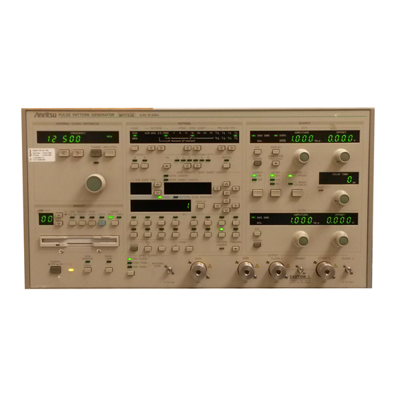
Related Manuals for Anritsu MP1763C


Summary of Contents for Anritsu MP1763C
- Page 1 Pulse Pattern Generator Service Manual Second Edition To ensure that the equipment is used safely, read the "For Safety" in the MP1763C Pulse Pattern Genera- tor Operation Manual first. Keep this manual with the equipment. ANRITSU CORPORATION Document No.: M-W1848BE-2.0...
- Page 2 BEFORE using the equipment. Some or all of the following five symbols may not be used on all Anritsu equipment. In addition, there may be other labels attached to products which are not shown in the diagrams in this manual.
- Page 3 Always request repair by a trained engineer who understands the haz- ards. Anritsu Corporation will not accept liability for any injuries sustained as a result of opening the equipment covers. WARNING Sure to read "For Safety" at the beginning of this manual before repair.
- Page 4 Notes On Export Management This product and its manuals require an Export License/Approval by the Government of the product's country of origin for re-export from your country. Before re-exporting the product or manuals, please contact us to confirm whether they are export-controlled items or not.
- Page 5 Power Line Fuse Protection For safety, Anritsu products have either one or two fuses in the AC power lines as requested by the customer when ordering. Single fuse: A fuse is inserted in one of the AC power lines. Double fuse: A fuse is inserted in each of the AC power lines.
- Page 7 About This Manual This service manual is used for the MP1763C Pulse Pattern Generator Composi- tion of the service manual: Service manual (M-W1848BE) Schematics (M-W1848GE) Service Manual: Describes circuit explanation, troubleshooting, adjustment, mechanical configuration, PC-board numbers/names, and circuit diagram num- bers.
-
Page 8: Table Of Contents
Table of Contents For Safety ........... About This Manual ........Section 1 Outline ........Section 2 Outline of Operation....General principles of operation ........Section 3 Troubleshooting ....... Introduction ..............Repair level ..............Location................. Measuring static electricity..........Service Kits ..............Equipment Required for Troubleshooting, Repair and Calibra-tion. -
Page 9: Outline
SECTION 6 MECHANICAL CONFIGURATION APPENDIX OVERALL CIRCUIT DIAGRAM For specifications, operating instructions, performance checks, and a detailed de- scription of the MP1763C Pulse Pattern Generator panel controls, refer to the sepa- rate operation manual. CAUTION Since the monolithic and hybrid ICs that are mounted in this instrument are very sensitive, be very careful when handling them. - Page 10 Section 1 Outline 1-2.
-
Page 11: Outline Of Operation
Section 2 Outline of Operation General principles of operation........2-2 2.1.1 Block diagram..........2-2 2.1.2 Data signal ............ 2-2 2.1.3 Clock signal ........... 2-2... -
Page 12: General Principles Of Operation
2.1.1 Block diagram Fig. 2-1 shows the MP1763C block diagram. 2.1.2 Data signal MP1763C consists of A08,A10,A09,A23 and E13 for Data signal. A08 PG generates the programmable pattern and pseudo-random pattern(128 bits of data) These 128 bits of data are multiplexed within the A10 MUX(L),A9 MUX(M) and A23 MUX(H) PKG and are then output via E13 DFF+OUT2 hybrid IC. - Page 13 2.1 General principles of operation...
- Page 14 Section 2 Outline of Operation 2-4.
-
Page 15: Troubleshooting
Section 3 Troubleshooting Introduction ..............3-2 Repair level..............3-2 Location ..............3-2 Measuring static electricity ........3-2 Service Kits..............3-2 Equipment Required for Troubleshooting, Repair and Calibration..........3-2 Overall Troubleshooting ..........3-3 3.7.1 Data signal problem ........3-3 3.7.2 Clock signal problem ........3-3 3.7.3 Waveform check method....... -
Page 16: Introduction
SECTION 3 describes how to troubleshoot the instrument when abnormalities occur during measurement or performance checks. 3.2 Repair level Repair of MP1763C is required just to replace PKG, UNIT or HIC. Adjustment will be required for some PKGs, UNITs and HICs. 3.3 Location Location of PKGs, UNITs and HICs are shown on page 3-6/3-7. -
Page 17: Overall Troubleshooting
This paragraph describes how to find a faulty section. 3.7.1 Data signal problem If the MP1763C does not output data signal, check waveform from at [1] to [11] of Fig 3-2. If it shows errors for both PROG and PRBS, check errors at [2],[4] and [6] of Fig 3-2 by using an Error Detector. - Page 18 Section 3 Troubleshooting Table 3-1 Service Kits Name Dwg.No. QTY. Diagram Extender 44Y98438 board 1 Extender 44Y98439 board 2...
- Page 19 3.8 Typical output waveform Table 3-1 Service Kits (Continued) Name Dwg.No. QTY. Diagram Extender 44Y98440 board 3 Extender 44Y98440B board 3B Extender 44Y98439 cable for SYNTHE...
- Page 20 Trigger count down Frequency rang:500MHz to 18 GHz Waveform MP1764A Error Detector Frequency rang:50MHz to 12.5 GHz Error rate (Anritsu) Probe Frequency rang: DC to 6 GHz Waveform ECL Terminator Frequency rang: DC to 10 GHz For monitoring the ECL level of...
- Page 21 3.8 Typical output waveform Location of HIC section...
- Page 22 Section 3 Troubleshooting MP1763C 12.5 GHzPPG Top View...
- Page 23 3.8 Typical output waveform...
-
Page 24: Typical Output Waveform
Section 3 Troubleshooting 3.8 Typical output waveform This paragraph shows typical output waveform of the MP1763C. 3.8.1 Data output Page 3-12 to 3-21 are Data output waveform with 50( termination. 3.8.2 Clock output Page 3-22 to 3-25 are Clock output waveform with 50( termination. -
Page 25: Zero Substitution Pattern
3.8 Typical output waveform 3.8.7 ZERO Substitution pattern When the ZERO sub. is selected, logical "1" bit is added just after the final bit of PRBS pattern, this pattern is pseudo-PRBS pattern(2 bits; N=7,9,11 or 15). Bits after the longest string of consecutive "0" of the pseudo-PRBS are substituted by"0"pattern. - Page 26 Section 3 Troubleshooting 3-12...
- Page 27 3.8 Typical output waveform 3-13...
- Page 28 Section 3 Troubleshooting 3-14...
- Page 29 3.8 Typical output waveform 3-15...
- Page 30 Section 3 Troubleshooting 3-16...
- Page 31 3.8 Typical output waveform 3-17...
- Page 32 Section 3 Troubleshooting 3-18...
- Page 33 3.8 Typical output waveform 3-19...
- Page 34 Section 3 Troubleshooting 3-20...
- Page 35 3.8 Typical output waveform 3-21...
- Page 36 Section 3 Troubleshooting 3-22...
- Page 37 3.8 Typical output waveform 3-23...
- Page 38 Section 3 Troubleshooting 3-24...
- Page 39 3.8 Typical output waveform 3-25...
- Page 40 Section 3 Troubleshooting 3-26...
- Page 41 3.8 Typical output waveform 3-27...
- Page 42 Section 3 Troubleshooting 3-28...
- Page 43 3.8 Typical output waveform 3-29...
- Page 44 Section 3 Troubleshooting 3-30...
- Page 45 3.8 Typical output waveform 3-31...
- Page 46 Section 3 Troubleshooting 3-32...
- Page 47 3.8 Typical output waveform 3-33...
- Page 48 Section 3 Troubleshooting 3-34...
- Page 49 3.8 Typical output waveform 3-35...
- Page 50 Section 3 Troubleshooting 3-36...
- Page 51 3.8 Typical output waveform 3-37...
- Page 52 Section 3 Troubleshooting 3-38.
-
Page 53: Waveform Check
Section 4 Waveform Check DC voltage check ............4-2 Waveform check ............4-2... -
Page 54: Dc Voltage Check
Section 4 Waveform Check 4.1 DC voltage check Before checking the waveforms, DC voltage of A07 power supply should be checked. Check DC voltage on A07 PCB referring the figure below. Check Point Adjustment Pot Adjustment Voltage +28V R151 +28.04V +15V R152 +15.15V... - Page 55 4.2 Waveform check...
- Page 56 Section 4 Waveform Check...
- Page 57 4.2 Waveform check...
- Page 58 Section 4 Waveform Check...
- Page 59 4.2 Waveform check...
- Page 60 Section 4 Waveform Check...
- Page 61 4.2 Waveform check...
- Page 62 Section 4 Waveform Check ⑪ A08 PG OUTPUT X1 to X16 on A08 ECL termination PRBS pattern 12.5 GHz 50 MHz 4-10...
- Page 63 4.2 Waveform check 4-11...
- Page 64 Section 4 Waveform Check ⑪ A08 PG OUTPUT X1 to X16 on A08 ECL termination PRBS pattern 12.5 GHz 50 MHz 4-12...
- Page 65 4.2 Waveform check 4-13...
- Page 66 Section 4 Waveform Check 4-14...
- Page 67 4.2 Waveform check 4-15...
- Page 68 Section 4 Waveform Check 4-16...
- Page 69 4.2 Waveform check 4-17...
- Page 70 Section 4 Waveform Check 4-18...
- Page 71 4.2 Waveform check 4-19...
- Page 72 Section 4 Waveform Check 4-20...
- Page 73 4.2 Waveform check 4-21...
- Page 74 Section 4 Waveform Check 4-22.
-
Page 75: Adjustment Procedure
Section 5 Adjustment Procedure Adjustment Procedure ..........5-2... - Page 76 Section 5 Adjustment Procedure 5.1 Adjustment Procedure This section describes adjustment for HICs. If output waveform of the HIC is not identical after replace HIC, perform adjustment by referring the procedure.
- Page 77 5.1 Adjustment Procedure Adjustment Procedure A23 MUX(H) Required equipment: Sampling oscilloscope. Waveform check method 50Ω Termination 1.Confirm the phase relation ship of D1 pin#7,1 and 5 shown in Fig-1. 2.Adjust R3 so that the duty cycle of the output waveform is 50%. 3.Adjust R6 so that the output waveform is nice and clean.
- Page 78 Section 5 Adjustment Procedure Adjustment Procedure A29 FREQ DIVIDER Required equipment: Sampling oscilloscope. Spectrum analyzer ECL level converter Waveform check method 50Ω Termination/ECL Termination 1.Confirm the phase relation ship of D1 pin#7,1 and 5 shown in Fig-1. 1. 1/2 Clock output (1) Input 12.5GHz, 2Vp-p signal into the A29, and connect a spectrum analyzer to X2.
- Page 79 5.1 Adjustment Procedure Adjustment Procedure A35 CLOCK INPUT BIAS PKG Required equipment: Sampling oscilloscope. Digital multi-meter. ** Two clock outputs must be observed simultaneously by the sampling oscilloscope ** 1. Input 12.5 GHz and 2.00Vp-p clock signal into E7 CLOCK INPUT HIC by external. signal generator or internal synthesizer.
- Page 80 Section 5 Adjustment Procedure Adjustment Procedure A38 CLOCK BRANCH HIC BIAS PKG Required equipment: Sampling oscilloscope. Digital multi-meter. ** Three clock outputs must be observed simultaneously by the sampling oscilloscope ** 1. Input 12.5 GHz and 2Vp-p clock signal into the HIC 2.
- Page 81 5.1 Adjustment Procedure Adjustment Procedure A42 DFF+OUT2 HIC BIAS equired equipment: Sampling oscilloscope. Digital multi-meter. Waveform check method 50Ω Termination 1.Confirm the phase relation ship of D1 pin#7,1 and 5 shown in Fig-1. 1. Confirm the voltage at X1 pin#11, X1 pin#12, X1 pin#15 and X1 pin #16 which are same voltage as front panel settings.
- Page 82 Section 5 Adjustment Procedure 5-8.
-
Page 83: Mechanical Configuration
Section 6 Mechanical Configuration Introduction ..............6-2 Disassembly .............. 6-2... - Page 84 Section 6 Mechanical Configuration 6.1 Introduction This section explains how to disassemble the MP1763C 6.2 Disassembly...
- Page 85 6.2 Disassembly Table 6-1 Mechanical Parts List for Fig. 6-1 Parts No. Description Remarks 422H16873 Front frame 1MW-5U 422H16870B Rear channel 43H34883C Protector 43H34883D Protector 422H16871 Top channel 450D 422H16872 Bottom channel 450D 349B73667 Standard foot 34B73660J Trim tape 349B73661K Side handle 450U [10]...
- Page 86 Section 6 Mechanical Configuration...
- Page 87 6.2 Disassembly Table 6-2 Mechanical Parts List for Fig. 6-2 Parts No. Description Remarks 423B18223L Front panel 422B16869 Sub panel 432B42904 Filter 442B100694B Filter 422B100717 Filter 422B100694 Filter 442B100719 Filter 442B100718B Filter [10] [11] 342E77920 Knob [12] 342E73702 Knob [13] 44H94174 Package clamp [14]...
- Page 88 Section 6 Mechanical Configuration...
- Page 89 6.2 Disassembly Table 6-3 Mechanical Parts List for Fig. 6-3 Parts No. Description Remarks 423B16408B Rear panel 424B17064C Fan cover 43H34883C Protector 43H34883D Protector 4NPS12S7 Screw 4NPS16S7 Screw 4WB-B3 Plain washer 3NPS6B3+SW Screw 3NPS8B3+SW Screw [10] 3FPS8B3 Screw [11] 2.6NPS8B3+SW Screw [12] 432B44756C...
- Page 90 Section 6 Mechanical Configuration...
- Page 91 6.2 Disassembly Table 6-4 Mechanical Parts List for Fig. 6-4 Parts No. Description Remarks 423B16417B Chassis 44B100428 Dust cover 44H55053E Support 44B94272 Stopper 3NPS6B3+SW Screw 3NPS14B3+SW Screw 3NPS30B3+SW+WB Screw 3FPS8B3 Screw 2.6NPS6B3+SW Screw...
- Page 92 Section 6 Mechanical Configuration 6-10...
- Page 93 6.2 Disassembly Table 6-5 Parts List of Keytop for Fig. 6-5 Parts No. Description Remarks 342E93472 Keytop 442E89108D Keytop < 442E89108C Keytop > 34E91902B Keytop Dark gray 34E91902 Keytop 342E91911 Keytop 34E91910 Keytop 34E91910D Keytop Blue 34E91910B Keytop Dark gray [10] 442E94246D Keytop...
- Page 94 Section 6 Mechanical Configuration 6-12.
-
Page 95: Appendix A Outline Of Operation
Appendix A Outline of Operation Block Diagram ............A-3 Module List ..............A-11... - Page 96 Appendix A Outline of Operation...
- Page 97 A.1 Block Diagram...
- Page 98 A.1 Block Diagram...
- Page 99 A.1 Block Diagram...
- Page 100 A.1 Block Diagram...
- Page 101 A.1 Block Diagram...
- Page 102 A.1 Block Diagram...
- Page 103 A.1 Block Diagram...
- Page 104 A.1 Block Diagram A-10...
-
Page 105: Module List
A.2 Module List A.2 Module List MP1763C PKG/MODULE LIST PKG/MODULE No. Drawing No. Remarks SYMTHE 44Y100047 Option Al-A1 CRYSTAL 44Y93822 Same PKG as MP1701B A1-A2 REF LOOP 44Y93823 Same PKG as MP1701B Al-A3 1kHz LOOP 44Y93824 Same PKG as MP1701B... - Page 106 Appendix A Outline of Operation MP1763C HIC LIST MODULE No. Drawing No. Remarks MHL61650A 6G AMP 44Y99902 MHL61660A 6G MUX 44Y99969 MHL61670A CLK BRANCH 44Y99971 MHL70860E DFF+OUT2 429H15651F MHL70810A CLK OUT 429H15017L MHL70031B CLK IN 429H15137D MHL70310A CLK BRANCH 429H15018C...
- Page 107 A.2 Module List *** PROG pattern output *** 1. 1/8 DATA OUTPUT and Panel setting. ** DATA length 128bits ** 1/8 output No. Correspond bit of setting DATA 1, 9, 17, 25, 33, 41, 49, 57, 65, 73, 81, 97, 105, 113, 121, 2, 10, 18, 26, 34, 42, 50, 58, 66, 74, 82, 98, 106, 114, 122, 3, 11, 19, 27, 35, 43, 51, 59, 67, 75, 83, 99, 107, 115, 123, 4, 12, 20, 28, 36, 44, 52, 60, 68, 76, 84, 100, 108, 116, 124,...
- Page 108 Appendix A Outline of Operation A-14.
Need help?
Do you have a question about the MP1763C and is the answer not in the manual?
Questions and answers