
Subscribe to Our Youtube Channel
Related Manuals for Tatung G5GS Series


Summary of Contents for Tatung G5GS Series
- Page 1 MODEL:C5GS SERIES Low Radiation Extended VGA PLUG & PLAY COLOUR MONITOR SERVICE MANUAL...
-
Page 2: Table Of Contents
TABLE OF CONTENTS PAGE 1. Precaution and Notices ..................1 2. Specifications ....................... 3 3. Control Location and Functions ............... 5 4. Disassembly Instructions ................... 7 5. General Connection & Applications ..............9 6. Electronic Circuit Description ................. 10 7. Adjustment ......................19 8. -
Page 3: Precaution And Notices
1. Precautions and Notices 1.1 Safety Precautions 1) Observe all cautions and safety related notes located inside the display cabinet and on the display chassis. 2) Operation of these displays outside the cabinet or with the cover removed involves a shock hazard from the display power supplies. - Page 4 1.2 Product Safety Notice 1) Many electrical and mechanical parts in this chassis provide special visual safety protection. The protection afforded by them cannot necessarily be obtained by using replacement components rated for higher voltage, wattage, etc. 2) Before replacing any of these components, read the parts list in this manual carefully. The use of substitute replacement parts which do not have the same safety characteristics as specified in the parts list may create shock, fire, X-Ray radiation or other hazards.
-
Page 5: Specifications
2. Specifications 2.1 Monitor Specification AC 100 ~ 240V , 50 / 60Hz Power Source LED color is green Normal Operation (Max.70W) Power LED color is amber Stand By / Suspend Mode (Max.15W) Consumption LED color is amber Off Mode (Max. - Page 6 2.2 Preset Timing Table(I) for HP Mode Resolution H-Freq. V-Freq. Hs. pol. Vs. pol. 720 x 400 31.47 kHz 70.08 Hz Negative (-) Positive (+) 640 x 480 31.47 kHz 59.95 Hz Negative (-) Negative (-) 640 x 480 35.16 kHz 56.25 Hz Negative (+/-) Negative (+/-) 800 x 600...
-
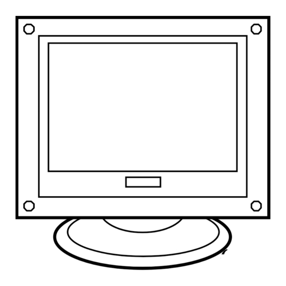
Page 7: Control Location And Functions
3. Control Location and Functions Front View Rear View 3. 4. 1. Indication LEDs 1. AC Power Plug 2. Control Buttons 2. Signal Cable 3. Power Switch's LED 4. Power Switch 3.1 Indication LEDs : When one of the digital controls is selected, the corresponding LED(s) are lit. CONTRAST : To adjust the contrast of the display. - Page 8 3.2 Control Buttons : The Select Button (the left button) selects a digital control. The selected control is indicated by the corresponding indication LED. The Down (down arrow) and UP (up arrow) buttons allow you to decrease or increase the value of the selected control. Press the Down (down arrow) and up (up arrow) simultaneously, Then it will degauss the display.
-
Page 9: Disassembly Instructions
4. Disassembly Instructions 1) Face Down the Monitor : ( Fig.4-1 ) 2) Swivel Base Removal : First press the stopper, then slide the swivel ball down and remove it. ( Fig.4-2 ) 3) Back Cover Removal : Remove 4 screws (A) ( Fig.4-3 ) and (B) (Fig. 4-4) from the back cover. Then remove the back cover. - Page 10 a) Unplug grounding connectors and the degaussing coil grounding connector from the CRT drive shield. b) Remove CRT drive board (C) from CRT neck. (Fig.4-5) c) Unplug the DY connector, AC connector, Degaussing coil connector and the CRT grounding connector from the FBT shield. d) Discharge the remaining static electricity by shorting CRT anode and ground, then remove the FBT anode connector.
-
Page 11: General Connection & Applications
5. General Connection & Applications Procedure for installing and using your Multi-Sync. display. 5.1 Connecting the monitor to the computer 1) Set up the display at the desired operation location , on top of or beside your personal computer. Plug the power cord into the monitor and then connect the other end of the power cord into an AC outlet. -
Page 12: Electronic Circuit Description
6 . Electronic Circuit Description 6.1 Switching Mode Power Supply ( SMPS ) The switching mode power supply for this monitor is a full range type, i.e. universal power input of AC 100V ~ 240V is compatible. When AC input is supplied through the slow blow fuse F801, the line choke L803 to the rectifier D811 ~ D814, the rectified DC voltage is about 125V ~ 335V and then fed to the switching transformer T801. - Page 13 If over-load or short circuit occurs at the secondary, the voltage across R825 and R823 reaches 1Vp-p rapidly, thereby blocking the power output, the voltage at pin7 of I801 then decrease to below 10V, I801 is forced off. However, in order to allow auto-recovery from power saving off state, the SMPS circuit is designed as an unlatched type, the DC current flows via R828, R831, Q813 and D828 to charge C808 again.
- Page 14 Heater Voltage The heater element in the CRT is supplied with 6.3±0.3V during normal operation and reduced to 5.0±0.5V during Stand By or Suspend state. To achieve this, Q805, Q806 and associated circuit is introduced, when at normal state, PM2 is HIGH level then Q805 ON, to trigger Q806 ON, 10V from D815 to Q806, R841, R991 and heater, the heater voltage is 6.3V±0.3V.
- Page 15 and pull-up resistor R208. The other control function is by I C-bus, the SCL and SDA signals are fed to pin30 and pin31 of deflection processor I401 via pin10 pin9 of I201. The CPU is reset by the components C204, C203 and D213 at pin4 of I201, when the AC source is connecting, every time to ensure correct start.
- Page 16 6.6 Deflection Processor 6.6.1 I401 is used for S1D2511B I401 S1D2511B is a Samsung monolithic integrated circuit assembled in a 32 pins shrunk dual in line plastic package. I401 controls all the functions related to the horizontal and vertical deflection in a multi-sync monitor.
- Page 17 6.7 Vertical Deflection Circuit The power amplifier drive the vertical yoke assembly is a DC design based on power amplifier I301 TDA8172. The TDA8172 consists of a differential input stage, two power supply (+10V and –11V), a flyback generator, a protection circuit for the output stages. The differential input stage has a high CMRR differential current mode input (pin6 and pin7 ).
- Page 18 When the horizontal frequency of input signal is greater then 42.4KHz, Q425 is on, Q424 is off, C415 is the only capacitor for S-shape correction. Input H. I201#17 Cs C415 C452 Frequency Fh < 42.4KHz 42.4KHz < Fh 6.9 Horizontal Width Control The monitor uses a diode modulation circuit for the control of horizontal width, it is achieved by changing the base voltage of Q418, the control voltage (0~ 5V) is from pin11 of I401 via R454, which consist of horizontal pincushion &...
- Page 19 6.14 H.V. Control Circuit The horizontal feedback signal derived from pin6 of T403 is applied via D403, R415, R420, R402, R416 and peak-detected by C474 and R492, then fed to the error amplifier on pin5 of I401, the value of R410 is chosen to have a suitable gain for the error amplifier. The saw-tooth waveform signal related to the output current of Q413 is fed to pin4 of I401 via R451 current...
- Page 20 6.15 Video Circuit The analog R. G. B. video input signals are supplied through the cable which is terminated at P501, these input signals are approximately 0.7 Vp-p in amplitude. R501/ R531/ R561 give a resistance of 75 ohm for impedance matching. The R. G. B. video signals are AC coupled via C501/ C531/ C561 then fed into the video pre-amplifier I501 at pin6, pin3 and pin1 respectively.
- Page 21 7. Adjustment PCB Main Parts Location MAIN BOARD ( Component Side View) PWB-0248 S202 D891 S201 D206....D201 D201~ D206—Display LED's D891—Power LED R420—H.V. Adjust R471—ABL Adjust S202—Power Switch • S202— Up Button • Down Button — R420 Select Button — T403—FBT T403 R471...
-
Page 22: Adjustment
7.3 High Voltage Adjustment a ) Apply a Super VGA signal ( 54KHz ) with crosshatch pattern. b ) Set the BRIGHTNESS control to 0.06FL and CONTRAST control to maximum. c ) Adjust H.V. Adj. R420 for the high voltage to be 25.0KV±0.2KV. 7.4 Auto Sizing Adjustment To enter into the factory setting mode, operate according the following procedure: Switch off the monitor first, push and hold the SELECT Button, power on again, wait 1.0 second... - Page 23 7.6 Focus Adjustment a ) Apply a 54KHz signal with crosshatch pattern. b ) Adjust FOCUS control on T403 to get the best overall focus. 7.7 Convergence Adjustment Note 1: For a unit with new ITC, adjustment for convergence may not be necessary. 2 : Prior to alignment procedures must be completed.
-
Page 24: Troubleshooting Flow Chart
8. Troubleshooting Flow Chart (1) Power Start NG Power start NG the voltage at C804 normal (125-340V) F801 open R808 open Check power socket copper and plug & D811•D814, Check Q801, I801 R804 the start-up voltage at C808>16V and Operation Voltage at C808 >... - Page 25 (2) No Data Appear No data appear the waveforms at pin 1,3,6 of I501 normal Check signal cable & C501, C531, C561 Are the voltages at pin 13 Check R471, D451, D404, I402, of I501 normal D401, R405, R404, R584. the waveforms at pin 14, 17, 20, of I501 normal...
- Page 26 No raster appear (3) No Raster Appear Is the H.V. correct the voltage at heater normal Check brightness Check Q403, Q413. Q403, Q413 (6.3V) circuit, Q402, Q406. short? Check spot killer Check R841, circuit: R991, CRT D302, D422. Socket Is the Check FBT, CRT.
- Page 27 R/G/B is Missing Loss of vertical synchronization (4) R/G/B is Missing (5) Loss of Vertical Synchronization Is the waveform Is the Check signal cable at pin 1, 3, 6 of waveform at C501, C531, C561 Check I401, R32 I501 normal pin 32 of I201 C301, R323, C304 normal ?
- Page 28 No vertical scanning Loss of horizontal synchronization (6) Loss of Horizontal Synchronization (7) No Vertical Scanning (One Horizontal Line) Deflection yoke is Is the Is the Check I401, R423, defective waveform at waveform at R433, pin 33 of I201 pin 5 of I301 R434, C412, R42 normal ? normal ?
- Page 29 Micro Control Abnormal (8) Micro Control Function Is the function LED Check R230, R231, working ? R257, S202. Check S201 – S202. Press UP or DOWN key, I202 is defective. can it adjustment H. Size Abnormal (9) Horizontal Width Control Abnormal Is H.size control function working...
-
Page 30: Block Diagram
9. BLOCK DIAGRAM I 801 R991 6.3V Heater T801 D815 L803, Q801 D819 100V• D811•D814 D808 D817 Q901, Q902 240V I501 EMI Filter Q812 D818 R. Video Output Video Rectifier Q828 D805 Pre-Amp. Q815 I401 Q931, Q932 V901 CRT G. Video Output SMPS H./V. -
Page 31: Electrical Parts List
12. Electrical Parts List WARNING : Replacement parts which have special characteristics important to safety should be replaced only with types identical to those in the original circuit or specified in the parts list. Before replacing any of these components, read carefully the product safety precautions. Do not degrade the safety of the display through improper servicing. - Page 32 C422 5231322291 CAPACITOR, CERAMIC 50V 2200.00PF K C423 5213610091 CAPACITOR, ELECTROLYTIC 50V 10.00UF M C424 5236310491 CAPACITOR, BARRIER LAYER 50V 0.10UF Z C428 5236310491 CAPACITOR, BARRIER LAYER 50V 0.10UF Z C429 5236310491 CAPACITOR, BARRIER LAYER 50V 0.10UF Z C432 5213447091 CAPACITOR, ELECTROLYTIC 25V 47.00UF M C434...
- Page 33 C828 RA 5270106201 CAPACITOR, METALLIZED 250V 0.22MF M C828 RB 5270109501 CAPACITOR, METALLIZED 275V 0.22MF K C830 RA 5230105001 CAPACITOR, CERAMIC 400V 4700.00PF M C830 RB 5230105501 CAPACITOR, CERAMIC 400V 4700.00PF M C831 RA 5230105001 CAPACITOR, CERAMIC 400V 4700.00PF M C831 RB 5230105501 CAPACITOR, CERAMIC...
- Page 34 D422 6613003032 DIODE, SWITCHING HIT 1N4148-TD 75V 150MA D431 RA 6613002244 DIODE, SWITCHING GIT RGP10D-G23 D431 RB 6613002249 DIODE, SWITCHING LIT PR1003G D439 6613003032 DIODE, SWITCHING HIT 1N4148-TD 75V 150MA D440 RA 6611027704 DIODE, RECTIFIER TSB 3GU41 D440 RB 6611027700 DIODE, RECTIFIER GIT UF5404 D448 RA...
- Page 35 I301 6644076000 IC,LINEAR VERTICAL DEF. ST TDA8172 I401 6644076302 IC,LINEAR A.S.D.C. SAM S1D2511B0-A0B0 I402 RA 6644008105 IC,LINEAR DUAL COMPARATOR ST LM358N I402 RB 6644008103 IC,LINEAR DUAL COMPARATOR TI LM358P I801 RA 6644063104 IC,LINEAR SAM KA3842B I801 RB 6644063111 IC,LINEAR ST UC3842BN I802 RA 6642002909 IC,PHOTO COUPLER...
- Page 36 Q424 RA 6626000603 TRANSISTOR, FET MOS TSB YTAF630 Q424 RB 6626004000 TRANSISTOR, FET MOS SYO 2SK2161 Q425 RA 6621026430 TRANSISTOR, NPN HF TSB BF422 Q425 RB 6621026434 TRANSISTOR, NPN HF KEC BF422 Q801 RA 6626005100 TRANSISTOR, FET MOS NEC 2SK2141 Q801 RB 6626000902 TRANSISTOR, FET MOS...
- Page 37 R225 5142151195 RESISTOR, CARBON FILM 1/6W 510.00 J R226 5142151195 RESISTOR, CARBON FILM 1/6W 510.00 J R228 5142110295 RESISTOR, CARBON FILM 1/6W 1.00K J R229 5142120295 RESISTOR, CARBON FILM 1/6W 2.00K J R230 5142110295 RESISTOR, CARBON FILM 1/6W 1.00K J R231 5142120295 RESISTOR, CARBON FILM...
- Page 38 R410 5142110595 RESISTOR, CARBON FILM 1/6W 1.00M J R411 5142110395 RESISTOR, CARBON FILM 1/6W 10.00K J R412 5142815295 RESISTOR, CARBON FILM 1/4W 1.50K J R413 5142118395 RESISTOR, CARBON FILM 1/6W 18.00K J R414 5142120395 RESISTOR, CARBON FILM 1/6W 20.00K J R415 5142891295 RESISTOR, CARBON FILM...
- Page 39 R465 5142815495 RESISTOR, CARBON FILM 1/4W 150.00K J R466 5142847395 RESISTOR, CARBON FILM 1/4W 47.00K J R467 5142122295 RESISTOR, CARBON FILM 1/6W 2.20K J R468 5142427190 RESISTOR, CARBON FILM 1/2W 270.00 J R469 5142810395 RESISTOR, CARBON FILM 1/4W 10.00K J R470 5142110395 RESISTOR, CARBON FILM...
- Page 40 R839 5142147395 RESISTOR, CARBON FILM 1/6W 47.00K J R840 5142110495 RESISTOR, CARBON FILM 1/6W 100.00K J R841 5130582903 RESISTOR, METAL OXIDE FILM 3W 8.20 J R842 5142847295 RESISTOR, CARBON FILM 1/4W 4.70K J R843 5142847295 RESISTOR, CARBON FILM 1/4W 4.70K J R844 5142147295 RESISTOR, CARBON FILM...
- Page 41 ASSEMBLY PCB-CRT DRIVE (PWB-0239) Ckt No. Part No. Description Specification Remarks C501 5236310491 CAPACITOR, BARRIER LAYER 50V 0.10UF Z C502 5236310491 CAPACITOR, BARRIER LAYER 50V 0.10UF Z C503 5236310491 CAPACITOR, BARRIER LAYER 50V 0.10UF Z C504 5236310491 CAPACITOR, BARRIER LAYER 50V 0.10UF Z C505 5236310491...
- Page 42 I501 6644069901 IC,LINEAR VIDEO PRE-AMP. MIT MM1375XD SDIP-22 L901 5064439929 COIL, PEAKING TRF-8399J L902 5064468929 COIL, PEAKING TRF-8689J L931 5064427929 COIL, PEAKING TRF-8279J L932 5064468929 COIL, PEAKING TRF-8689J L961 5064439929 COIL, PEAKING TRF-8399J L962 5064468929 COIL, PEAKING TRF-8689J L991 5062202300 COIL, HOR CHOKE TLN-2026 P501...
- Page 43 R564 5142833095 RESISTOR, CARBON FILM 1/4W 33.00 J R565 5142168095 RESISTOR, CARBON FILM 1/6W 68.00 J R566 5142139195 RESISTOR, CARBON FILM 1/6W 390.00 J R567 5142833095 RESISTOR, CARBON FILM 1/4W 33.00 J R580 5142156395 RESISTOR, CARBON FILM 1/6W 56.00K J R581 5142191295 RESISTOR, CARBON FILM...
- Page 44 Z902 5202200502 SPARK GAP P=5MM 1-2KV 1PF Z903 5202201991 SPARK GAP DSP-201M-C04F DC200V 1PF Z933 5202201991 SPARK GAP DSP-201M-C04F DC200V 1PF Z963 5202201991 SPARK GAP DSP-201M-C04F DC200V 1PF CRT / ACCESSORY / MISCELLANEOUS Ckt No. Part No. Description Specification Remarks F801 5054431539 FUSE...
-
Page 45: Mechanical Parts List
14. Mechanical Parts List DESCRIPTION PART NO FRONT COVER 5642283100(HP) FRONT COVER 5642283101 FRONT COVER 5642283102(RM) FRONT COVER 5642283103(CLI) 5642843100(HP) POWER KEY 5642843101 COMPRESSION SPRING 5644200300 POWER LIGHT PIPE 5640326800 5642843200(HP) FUNCTION KEY 5642843201 FUNCTION LIGHT PIPE 5640326900 DRIVE CARD SHIELD 5646248500 SPONGE 5642018215...
Need help?
Do you have a question about the G5GS Series and is the answer not in the manual?
Questions and answers