Table of Contents
Advertisement
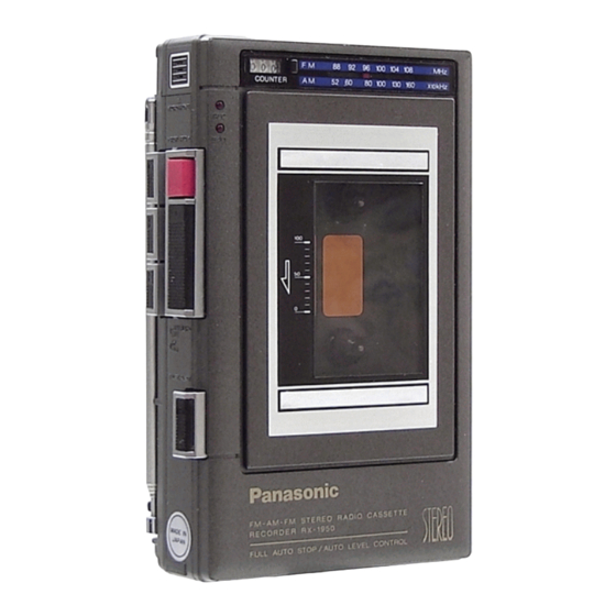
RX-1950
RX-1950
SCHEMATIC DIAGRAM MODEL RX-1950
IC1
IC2
arg
Ic3
pe
Notes:
AN7213
MA15OFV 2
1. $1:
Band
selector
switch in "FM" Position.
FM FRONT END
"
2sK160
anne Goan 2801623 RVDPR24340 RVILA3365
—_OA90_
(...FM, 3...AM).
(2...Tape, 3...Radio)
3. S3-1, S3-2:
Mode switch in ''Stereo" Position.
(2...Stereo, 3... Mono)
4. S4-1, S4-2:
Tape selector switch in "Normal" Position.
(2...Normal, 3...Metal)
5. S5-1~S5-8:
R/P switch in ""PLayback"' Position.
(2...Playback, 3...Record)
e 4'] on Cee
6. S6:
Motor switch.
7. VR1...... Balance control, VR2...... Voume control
(4)
VT1......VCO Adjustment, VT2......Bias current
a
Lt,
Adjustment
|
8. DC voltage measurement are taken with electronics volt-
meter from negative terminal of battery.
[
]...FM position, (
)...AM position
9. Battery current, NoSignal
...........c.cccceeceeceeeeeceees 47MA
Maximum Output (Radio) ecdcatuncios 65mA
BOTTOM VIEW
Sf
(ood)
213213
CO)
3
|
: Turse] Y T ]
DC IN
SeSr[seesee S2-2
| S6
part = §
? Seals 000000
|S?2.-4
|
(6V) =
T
s2[ 208
Ss
64 344 000
S4 oy. (eee
$5-2_S5-3
S5-4
TEEERERSE
S5-5 $5-6 $5-7 S5-8
ty
ae)
Cq10V
220
Sh 390
Ro)J270
ELECTRONIC
GOVERNOR
$5
=
IC BLOCK DIAGRAM
RVDPR2434D
IC3 RVILA3365
ESTE IND
10
RVDPR2434D ©
REC IND
D11
R109
470
|
REGULA
aa
pari
Ses
Q4.5
Q10~12
Q6~9
D4, 5
D6, 7
Q13, 16
Q14, 17
Q15, 18
Q20
Q21
@
2801623
2801623
2501623
MAt 193
MA27WB
28C1623
2SD601
2S8B709
2801623
MA27WB
280945
REC AMP
AGC
DRIVER
POWER AMP
POWERAMP ~~ SWITCHING
AOC
BIAS OSC
Ic2 AN7220A
AMIE FM IF
Vian
ee
|
Cathode
SD
SS
ie
Anode
S
:
Anoce
|
Cathode
OD
IC1
Ql, 3~20
D1, 11,6, 7,9
02
D4, 5
Q2
Advertisement
Table of Contents


Need help?
Do you have a question about the RX-1950 and is the answer not in the manual?
Questions and answers