Table of Contents
Advertisement
Quick Links
Advertisement
Table of Contents

Subscribe to Our Youtube Channel
Related Manuals for Clevo P955ET1


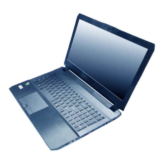
Summary of Contents for Clevo P955ET1
- Page 1 P955ET1 / P955ET3...
- Page 3 Preface Notebook Computer P955ET1 / P955ET3 Service Manual...
- Page 4 Preface Notice The company reserves the right to revise this publication or to change its contents without notice. Information contained herein is for reference only and does not constitute a commitment on the part of the manufacturer or any subsequent ven- dor.
- Page 5 This manual is intended for service personnel who have completed sufficient training to undertake the maintenance and inspection of personal computers. It is organized to allow you to look up basic information for servicing and/or upgrading components of the P955ET1 / P955ET3 series notebook PC.
- Page 6 Preface IMPORTANT SAFETY INSTRUCTIONS Follow basic safety precautions, including those listed below, to reduce the risk of fire, electric shock and injury to per- sons when using any electrical equipment: 1. Do not use this product near water, for example near a bath tub, wash bowl, kitchen sink or laundry tub, in a wet basement or near a swimming pool.
- Page 7 Preface Instructions for Care and Operation The notebook computer is quite rugged, but it can be damaged. To prevent this, follow these suggestions: Don’t drop it, or expose it to shock. If the computer falls, the case and the components could be damaged. Do not expose the computer Do not place it on an unstable Do not place anything heavy...
- Page 8 Preface Avoid interference. Keep the computer away from high capacity transformers, electric motors, and other strong mag- netic fields. These can hinder proper performance and damage your data. Take care when using peripheral devices. Use only approved brands of Unplug the power cord before peripherals.
- Page 9 Preface Battery Precautions • Only use batteries designed for this computer. The wrong battery type may explode, leak or damage the computer. • Do not continue to use a battery that has been dropped, or that appears damaged (e.g. bent or twisted) in any way. Even if the computer continues to work with a damaged battery in place, it may cause circuit damage, which may possibly result in fire.
- Page 10 Preface Related Documents You may also need to consult the following manual for additional information: User’s Manual on CD/DVD This describes the notebook PC’s features and the procedures for operating the computer and its ROM-based setup pro- gram. It also describes the installation and operation of the utility programs provided with the notebook PC. System Startup 130°...
-
Page 11: Table Of Contents
Preface Contents Introduction ..........1-1 Bottom ................... A-4 Main Board ................... A-5 Overview ..................1-1 HDD ....................A-6 Specifications ..................1-2 LCD ....................A-7 External Locator - Top View with LCD Panel Open ......1-4 Schematic Diagrams......... B-1 External Locator - Front & Right Side Views .........1-5 External Locator - Left Side &... - Page 12 Preface IFP I/O Interface ................B-27 VCore & VCCGT & VCCSA ............B-59 Misc - GPIO, I2C and ROM ............B-28 VCore Output ................B-60 GPU NVVDD, FBVDDQ ............B-29 VCCGT, VCCSA Output .............B-61 GPU GND & Sequence ..............B-30 VNVVDD 1 ..................B-62 PCH 1/9 ..................
-
Page 13: Introduction
Chapter 1: Introduction Overview This manual covers the information you need to service or upgrade the P955ET1 / P955ET3 series notebook computer. Information about operating the computer (e.g. getting started, and the Setup utility) is in the User’s Manual. Information about dri-vers (e.g. -
Page 14: Specifications
Introduction Specifications Processor Options Video Adapter Options i7-8750H (2.20GHz) Microsoft Hybrid Graphics Mode 9MB Smart Cache, 14nm, DDR4-2666MHz, TDP 45W Supports up to 4 Active Displays Supports NVIDIA Surround View via HDMI x 1 and MiniDP x2 Core Logic Latest Specification Information Intel Integrated GPU Intel®... - Page 15 Introduction Audio Interface Environmental Spec High Definition Audio Compliant Interface Three USB 3.0 (USB 3.1 Gen 1) Type-A Ports (Including one Temperature AC/DC Powered USB Port) ° ° S/PDIF Digital Output Operating: 5 C - 35 Two USB 3.1 Gen 2 Type-C Ports* Sound Blaster®...
-
Page 16: External Locator - Top View With Lcd Panel Open
Introduction External Locator - Top View with LCD Panel Open Figure 1 Top View 1. PC Camera 2. *PC Camera LED *When the PC camera is in use, the LED will be illuminated. 3. Built-In Array Microphone 4. LCD 5. Speakers 6. -
Page 17: External Locator - Front & Right Side Views
Introduction External Locator - Front & Right Side Views Figure 2 Front View 1. LED Indicator FRONT VIEW Figure 3 Right Side View 1. Microphone-In Jack 2. Headphone & S/ PDIF Combo RIGHT SIDE VIEW Jack 3. USB 3.0 (USB 3.1 Gen 1) Ports 4. -
Page 18: External Locator - Left Side & Rear View
Introduction External Locator - Left Side & Rear View Figure 4 Left Side View 1. Security Lock Slot 2. Vent 3. DC-In Jack LEFT SIDE VIEW 4. HDMI-Out Port 5. Mini DisplayPorts 6. USB 3.1 Gen 2 Type-C Ports 7. USB 3.0 (USB 3.1 Gen 1) Ports 8. -
Page 19: External Locator - Bottom View
Introduction External Locator - Bottom View Figure 6 Bottom View 1. Vent 2. RJ-45 LAN Jack 3. USIM Card Reader (for 3G/ 4G USIM Cards) Overheating To prevent your com- puter from overhea- ting, make sure no- thing blocks any vent while the computer is in use. -
Page 20: Mainboard Overview - Top (Key Parts)
Introduction Mainboard Overview - Top (Key Parts) Figure 7 Mainboard Top Key Parts 1. KBC-ITE IT8587 1 - 8 Mainboard Overview - Top (Key Parts) -
Page 21: Mainboard Overview - Bottom (Key Parts)
Introduction Mainboard Overview - Bottom (Key Parts) Figure 8 Mainboard Bottom Key Parts 1. Mini-Card Connector (M.2 3G/SATA Module) 2. Mini-Card Connector (M.2 PCIE/SATA SSD Module) 3. Mini-Card Connector (WLAN Module) 4. PCH 5. GPU-GTX1060M 6. Memory Slots DDR4 SO-DIMM 7. -
Page 22: Mainboard Overview - Top (Connectors)
Introduction Mainboard Overview - Top (Connectors) Figure 9 Mainboard Top Connectors 1. DC-In Jack 2. HDMI Port 3. Mini Display Ports 4. USB 3.1 Gen 2 Type-C Ports 5. TP Connector 6. Keyboard Cable Connector 7. Microphone-In Jack 8. Headphone & S/ PDIF Combo Jack 9. -
Page 23: Mainboard Overview - Bottom (Connectors)
Introduction Mainboard Overview - Bottom (Connectors) Figure 10 Mainboard Bottom Connectors 1. USIM Card Reader (for 3G/4G USIM Cards) 2. Battery Connector 3. HDD Connector 4. Fan Connector 5. LCD Cable Connector 6. CCD Connector Mainboard Overview - Bottom (Connectors) 1 - 11... - Page 24 Introduction 1 - 12...
- Page 25 Introduction Mainboard Overview - Bottom (Connectors) 1 - 13...
- Page 26 Introduction 1 - 14 Mainboard Overview - Bottom (Connectors)
-
Page 27: Disassembly
Chapter 2: Disassembly Overview This chapter provides step-by-step instructions for disassembling the P955ET1 / P955ET3 series notebook’s parts and subsystems. When it comes to reassembly, reverse the procedures (unless otherwise indicated). We suggest you completely review any procedure before you take the computer apart. -
Page 28: Maintenance Tools
Disassembly NOTE: All disassembly procedures assume that the system is turned OFF, and disconnected from any power supply (the battery is removed too). Maintenance Tools The following tools are recommended when working on the notebook PC: • M3 Philips-head screwdriver •... -
Page 29: Maintenance Precautions
Disassembly Maintenance Precautions The following precautions are a reminder. To avoid personal injury or damage to the computer while performing a re- moval and/or replacement job, take the following precautions: Power Safety Don't drop it. Perform your repairs and/or upgrades on a stable surface. If the computer falls, the case and other components Warning could be damaged. -
Page 30: Disassembly Steps
Disassembly Disassembly Steps The following table lists the disassembly steps, and on which page to find the related information. PLEASE PERFORM THE DISASSEMBLY STEPS IN THE ORDER INDICATED. To remove the Keyboard: To remove the 4G Module: 1. Remove the keyboard page 2 - 5 1. -
Page 31: Removing The Keyboard
Disassembly Removing the Keyboard Figure 1 Keyboard Removal 1. Turn off the computer, turn it over. 2. Remove screws from the bottom of the computer. a. Remove the screws from 3. Open it up with the LCD on a flat surface before pressing at point to release the keyboard module (use the spe- the bottom of the compu- cial eject stick... -
Page 32: Removing The Battery
Disassembly Removing the Battery Figure 2 Battery Removal 1. Turn the computer off, and remove the keyboard (page 2 - 2. Remove screws (Figure 2a). a. Remove the screws. 3. Remove the SD card cover and screws (Figure 2b). b. Remove the SD cover 4. - Page 33 Disassembly 5. The battery will be visible at point on the computer (Figure 3d Figure 3 6. Carefully disconnect the cable , then remove screws (Figure 3e Battery Removal 7. Lift the battery off the computer (Figure 3f (cont’d.) 8. Reverse the process to install a new battery (do not forget to replace all the screws and bottom cover). d.
-
Page 34: Removing The Hard Disk Drive
Disassembly Removing the Hard Disk Drive Figure 4 HDD Assembly The hard disk drive can be taken out to accommodate other 2.5" serial (SATA) hard disk drives with a height of 7mm Removal (h). Follow your operating system’s installation instructions, and install all necessary drivers and utilities (as outlined in Chapter 4 of the User’s Manual) when setting up a new hard disk. - Page 35 Disassembly 4. Slightly slide and pull the hard disk out Figure 5 5. Lift the hard disk assembly out of the bay (Figure 5c HDD Assembly 6. Remove screws and bracket from the hard disk (Figure 5d Removal (cont’d.) 7. Reverse the process to install a new hard disk (do not forget to replace the screws). c.
-
Page 36: Removing The System Memory (Ram)
Disassembly Removing the System Memory (RAM) Figure 6 RAM Module The computer has four memory sockets for 260 pin Small Outline Dual In-line Memory Modules (SO-DIMM) support- Removal ing DDR4 Up to 2400 MHz. The main memory can be expanded up to 64GB. The total memory size is automatically detected by the POST routine once you turn on your computer. -
Page 37: Removing The M.2 Ssd Module
Disassembly Removing the M.2 SSD Module Figure 7 M.2 SSD-1 Module M.2 SSD-1 Removal Procedure Removal 1. Turn off the computer, turn it over, remove the battery (page 2 - 2. The M.2 SSD module will be visible at point on the mainboard (Figure 7a). -
Page 38: Removing The Wireless Lan Module
Disassembly Removing the Wireless LAN Module Figure 8 Wireless LAN 1. Turn off the computer, turn it over, remove the battery (page 2 - Module Removal 2. The Wireless LAN module will be visible at point on the mainboard (Figure 8a). -
Page 39: Wireless Lan, Combo, & Lte Module Cables
Disassembly Wireless LAN, Combo, & LTE Module Cables Note that the cables for connecting to the antennae on WLAN, WLAN & Bluetooth Combo, and LTE modules are not labelled. The cables/covers (each cable will have either a black or transparent cable cover) are color coded for identifi- cation as outlined in the table below. -
Page 40: Removing The 4G Module
Disassembly Removing the 4G Module Figure 9 4G Module Removal Procedure 4G Module Removal 1. Turn off the computer, remove the battery (page 2 - a. Locate the module. 2. Locate the module, it is visible at point Figure 9a b. -
Page 41: Removing The Ccd
Disassembly Removing the CCD Figure 10 CCD Removal 1. Turn off the computer, turn it over to remove the battery (page 2 - 2. Lay the computer down on a flat surface with the top case up forming a 130 degree angle. Carefully remove the a. - Page 42 Disassembly 5. Disconnect the cable (Figure 11c). Figure 11 6. Remove the CCD module (Figure 11d). CCD Removal 7. Reverse the process to install a new CCD module. (cont’d) c. Disconnect the cable. d. Remove the CCD mod- ule. 11.
-
Page 43: Part Lists
Appendix A:Part Lists This appendix breaks down the P955ET1 / P955ET3 series notebook’s construction into a series of illustrations. The component part numbers are indicated in the tables opposite the drawings. Note: This section indicates the manufacturer’s part numbers. Your organization may use a different system, so be sure to cross-check any relevant documentation. -
Page 44: Part List Illustration Location
Part List Illustration Location The following table indicates where to find the appropriate part list illustration. Table A - 1 Part List Illustration Part Location page A - 3 Bottom page A - 4 page A - 5 Main Board page A - 6 page A - 7 A - 2... -
Page 45: Top
Figure A - 1 Top A - 3... -
Page 46: Bottom
Bottom Figure A - 2 Bottom A - 4 Bottom... -
Page 47: Main Board
Main Board Figure A - 3 Main Board Main Board A - 5... -
Page 48: Hdd
Figure A - 4 A - 6 HDD... -
Page 49: Lcd
Figure A - 5 LCD A - 7... - Page 50 A - 8...
-
Page 51: Schematic Diagrams
Schematic Diagrams Appendix B: Schematic Diagrams This appendix has circuit diagrams of the P955ET1 / P955ET3 notebook’s PCB’s. The following table indicates where to find the appropriate schematic diagram. Diagram - Page Diagram - Page Diagram - Page Diagram - Page... -
Page 52: System Block Diagram
Schematic Diagrams System Block Diagram 1.25V(VDDQ),0.6VS P950EP/ER Coffee Lake System Block Diagram P950EP M/B BOARD VPP 2.5V SHEET 57 PCBA:6-7P-P95E8-002 PCB:6-71-P95E0-D02A VDD3,VDD5 BOM:6-77-P950ER00-D02A BOM:6-77-P950EP60-D02A SHEET 52 BOM: DDR4/1.2V/2400MHz BOM: 5V,3.3V,5VS,3VS, BOM: SHEET 2~65 PCIE*16 <=4.5" SHEET 51 27 MHz <=4.5" Coffee Lake-H P950HP CLICK BOARD PCB:6-71-P95E2-D04... -
Page 53: Processor 1/7
Schematic Diagrams Processor 1/7 U172C PEG_TX_0 C718 0.22u_10V_X5R_04 PEG_RX0 PEG_RXP_0 PEG_TXP_0 PEG_TX0 14 PEG_TX#_0 C716 0.22u_10V_X5R_04 PEG_RX#0 PEG_RXN_0 PEG_TXN_0 PEG_TX#0 14 PEG_TX_1 C719 0.22u_10V_X5R_04 PEG_RX1 PEG_TX1 14 PEG_RXP_1 PEG_TXP_1 PEG_TX#_1 C717 0.22u_10V_X5R_04 PEG_RX#1 PEG_RXN_1 PEG_TXN_1 PEG_TX#1 14 PEG_TX_2 C715 0.22u_10V_X5R_04 PEG_RX2 PEG_TX2 14 PEG_RXP_2... -
Page 54: Processor 2/7
Schematic Diagrams Processor 2/7 U172D Zdiff=85 DDI1_TXP_0 DDI1_TXN_0 EDP_TXP_0 EDP_TXP0 11 EDP_TXN0 DDI1_TXP_1 EDP_TXN_0 DDI1_TXN_1 EDP_TXP_1 EDP_TXP1 11 EDP_TXN1 DDI1_TXP_2 EDP_TXN_1 EDP_TXP2 11 DDI1_TXN_2 EDP_TXP_2 DDI1_TXP_3 EDP_TXN_2 EDP_TXN2 EDP_TXP3 11 DDI1_TXN_3 EDP_TXP_3 EDP_TXN_3 EDP_TXN3 EDP_AUX DDI1_AUXP EDP_AUXP DDI1_AUXN EDP_AUXN EDP_AUX# DDI2_TXP_0 DDI2_TXN_0 EDP_DISP_UTIL... - Page 55 Schematic Diagrams Processor 3/7 M_A_DQ[63:0] M_B_DQ[63:0] U172A U172B M_A_DQ0 M_B_DQ0 BT11 DDR0_DQ_0/DDR0_DQ_0 DDR0_CKP_0/DDR0_CKP_0 M_A_DIM0_CK_DDR0_DP DDR1_DQ_0/DDR0_DQ_16 DDR1_CKP_0/DDR1_CKP_0 M_B_DIM0_CK_DDR0_DP M_A_DQ1 M_B_DQ1 BR11 DDR0_DQ_1/DDR0_DQ_1 DDR0_CKN_0/DDR0_CKN_0 M_A_DIM0_CK_DDR0_DN DDR1_DQ_1/DDR0_DQ_17 DDR1_CKN_0/DDR1_CKN_0 M_B_DIM0_CK_DDR0_DN M_A_DQ2 M_B_DQ2 DDR0_DQ_2/DDR0_DQ_2 DDR0_CKP_1/DDR0_CKP_1 M_A_DIM0_CK_DDR1_DP DDR1_DQ_2/DDR0_DQ_18 DDR1_CKP_1/DDR1_CKP_1 M_B_DIM0_CK_DDR1_DP M_A_DQ3 M_B_DQ3 M_A_DIM0_CK_DDR1_DN M_B_DIM0_CK_DDR1_DN M_A_DQ4 DDR0_DQ_3/DDR0_DQ_3 DDR0_CKN_1/DDR0_CKN_1 M_B_DQ4 DDR1_DQ_3/DDR0_DQ_19...
- Page 56 Schematic Diagrams Processor 4/7 INTERNAL USE ONLY * ALL CFG 1 = NO TERMAINATION ON BOARD DEFAULT HIGH NEAR CPU * ALL CFG 0 = PHYSICAL STRAP LOW ON BOARD CFG 1.0V DESCRIPTION 1.05V_VCCST NORM STALL U172E NORM PCHLESS PCHLESS MODE NORM REVERSE PEG_LANE_REVERSAL -SEE PCIE CHAPTER...
- Page 57 Schematic Diagrams Processor 5/7 CRB:6XBULK (SMC7343D), 12X0603 (22UF), 42X0402(10UF), 48X0201(1UF), 3X0805(47UF) P950HX:0XBULK (SMC7343D), 6X0603 (22UF), 12X0402(10UF), 24X0201(1UF), 1X0805(47UF) VCORE VCORE PLACE CAPS AT BOARD EDGE PLACE CAPS AT BACK VCORE VCORE VCORE VCORE U172I U172J AA13 AH13 CPU_TOP_VCCCORE CPU_BACK_VCCCORE VCC1 VCC64 AA31 AH14...
- Page 58 Schematic Diagrams Processor 6/7 VDDQ VCCSA U172L 11.1A U172M VCCSA1 VDDQ1 AE12 VCCSA2 VDDQ2 VCCSA3 VDDQ3 RSVD_TP_5 VCCSA4 VDDQ4 IST_TRIG RSVD_TP5 VCCSA5 VDDQ5 IST_TRIG RSVD_TP_4 VCCSA6 VDDQ6 RSVD_TP4 RSVD_TP_3 AJ12 VCCSA7 VDDQ7 RSVD_TP3 AL11 VCCSA8 VDDQ8 RSVD_TP_1 BK28 VCCSA9 VDDQ9 RSVD_TP1 RSVD11 RSVD_TP_2...
-
Page 59: Processor 7/7
Schematic Diagrams Processor 7/7 VCCGT VCCGT U172G U172H U172F BJ15 U172K VSS_163 VSS_244 VSS_325 VSS_409 AY12 BJ18 AT14 BD35 VSS_1 VSS_82 VSS_164 VSS_245 VSS_326 VSS_410 VCCGT1 VCCGT80 AL10 AY33 BJ22 BP12 AT31 BD36 VSS_2 VSS_83 VSS_165 VSS_246 VSS_327 VSS_411 VCCGT2 VCCGT81 AL12 AY34... -
Page 60: Ddr4 Cha So-Dimm_0
Schematic Diagrams DDR4 CHA SO-DIMM_0 Channel A SO-DIMM 0[RAM1] STD TYPE VDDQ VTT_MEM J_DIMMA_1B H=4mm J_DIMMA_1A 2.5V VDD19 M_A_DQ[63:0] M_A_DQ5 VDD18 M_A_DIM0_CK_DDR0_DP CK0_T VDD17 M_A_DQ0 M_A_DIM0_CK_DDR0_DN CK0_C VDD16 VPP2 M_A_DQ2 M_A_DIM0_CK_DDR1_DP CK1_T VDD15 VPP1 M_A_DQ3 M_A_DIM0_CK_DDR1_DN CK1_C M_A_DQ1 VDD14 VDD13 M_A_DQ4 3.3VS M_A_DIM0_CKE0... -
Page 61: Ddr4 Chb So-Dimm_0
Schematic Diagrams DDR4 CHB SO-DIMM_0 Channel B SO-DIMM 0[RAM2] RSV TYPE J_DIMMB_1B VDDQ VTT_MEM H=4mm VDD19 2.5V VDD18 J_DIMMB_1A VDD17 M_B_DQ[63:0] VDD16 VPP2 M_B_DQ0 M_B_DIM0_CK_DDR0_DP CK0_T VDD15 VPP1 M_B_DQ5 M_B_DIM0_CK_DDR0_DN CK0_C VDD14 M_B_DQ7 M_B_DIM0_CK_DDR1_DP CK1_T M_B_DQ3 VDD13 3.3VS M_B_DIM0_CK_DDR1_DN CK1_C VDD12 M_B_DQ4 VDD11... -
Page 62: Panel, Inverter
Schematic Diagrams Panel, Inverter PANEL CONNECTOR (For coaxial cable) PANEL POWER (PLVDD) PLVDD 3.3VS C988 C281 U176 HW /SW G5016 0.1u_16V_X7R_04 J_LCD1 1u_6.3V_X5R_04 HW /SW PANEL PLVDD PLVDD OUT1 OUT2 OUT1 OUT2 C728 C286 R377 FRAME_LOCK#_R PLVDD_CT1 PLVDD_CT1 *1u_6.3V_X5R_04 10u_6.3V_X5R_06 *100K_04 C280 PANEL... -
Page 63: Mini Dp Port
Schematic Diagrams Mini DP Port mini-Display Port F (back) mini-Display Port E (back) Zdiff=90 Close to Display PORT SHIELD6 GND4 SHIELD6 GND4 COMMON COMMON SHIELD5 GND3 SHIELD5 GND3 D_MDP_F#3 C940 0.1u_16V_X7R_04 MDP_F#3 D_MDP_F3 C942 0.1u_16V_X7R_04 MDP_F_PW R MDP_E_PW R MDP_F3 DP_TDB_AUX#_F DP_TDB_AUX#_E AUX_CHN... -
Page 64: Hdmi Connector
Schematic Diagrams HDMI Connector HDMI CONNECTOR For ESD HDMI_5VS SY6288DAAC HDMI_5VS HDMI 3 / 2 1 S M T VOUT J_HDMI1 C814 C843 C851 *10u_6.3V_X5R_06 22u_6.3V_X5R_06 22u_6.3V_X5R_06 RB751V-40(lision) HDMI HDMI HDMI HDMI 12,51 SUSB HDMI_HPD-C HOT PLUG DETECT uP7549UMA5-20 PCB Footprint = M-SOT23-5 DDC/CEC GND HDMI_SDA-C R171... -
Page 65: Vga Pci Express
Schematic Diagrams VGA PCI Express NV PCI EXPRESS NV3V3 29,61 NVVDD_PWRGD 10K_04 2SK3018S3 CLK_REQ9_PEG# INS143952840 BGA2152 COMMON 1/23 PCI_EXPRESS PEX_VDD under GPU PLACE btw GPU & VR BB33 PEX_DVDD BK26 BB35 PEX_RST PEX_DVDD DGPU_PEX_RST# BB36 C116 C130 C102 C107 C292 C178 PEX_DVDD PEX_CLKREQ#... -
Page 66: Gpu Frame Buffer Partition
Schematic Diagrams GPU Frame Buffer Partition PAGE3: GPU FRAME BUFFER PARTITION A/B INS143814845 BGA2152 INS143815523 COMMON BGA2152 COMMON 3/23 FBB 2/23 FBA FBB_D0 FBB_CMD0 FBB_D0 FBB_CMD0 FBA_D0 FBA_CMD0 FBA_DBI[7..0] FBB_DBI[7..0] FBB_D1 FBB_CMD1 FBA_D0 FBA_CMD0 FBA_DBI[7..0] FBB_DBI[7..0] FBB_D1 FBB_CMD1 FBA_D1 FBA_CMD1 FBB_D2 FBB_CMD2 FBA_D1... -
Page 67: Frame Buffer Partition A
Schematic Diagrams Frame Buffer Partition A FBA_WCK01 FBA_CMD[31..0] FBA_W CK01 FBA_CMD[31..0] FBA_WCK01# FRAME BUFFER PARTITION A FBA_W CK01# FBA_WCK23 FBA_D[63..0] FBA_W CK23 FBA_D[63..0] FBA_WCK23# FBA_W CK23# FBA_WCK45 FBA_DBI[7..0] P95xEP6,P95xER VRAM=K4G80325FB-HC25 Value:K4G80325FB-HC25 FBA_W CK45 FBA_DBI[7..0] FBA_WCK45# FBA_W CK45# FBA_WCK67 FBA_EDC[7..0] P95xEP3 VRAM=K4G41325FE-HC25 Value:K4G41325FE-HC25 FBA_W CK67 FBA_EDC[7..0] FBA_WCK67#... -
Page 68: Frame Buffer Partition B
Schematic Diagrams Frame Buffer Partition B FRAME BUFFER PARTITION B FBB_WCK01 FBB_CMD[31..0] FBB_W CK01 FBB_WCK01# FBB_CMD[31..0] FBB_W CK01# FBB_WCK23 FBB_D[63..0] FBB_W CK23 FBB_D[63..0] FBB_WCK23# P95xEP6,P95xER VRAM=K4G80325FB-HC25 Value:K4G80325FB-HC25 FBB_W CK23# FBB_WCK45 FBB_DBI[7..0] FBB_W CK45 FBB_WCK45# FBB_DBI[7..0] P95xEP3 VRAM=K4G41325FE-HC25 Value:K4G41325FE-HC25 FBB_W CK45# FBB_WCK67 FBB_EDC[7..0] FBB_W CK67... -
Page 69: Frame Buffer Partition A_B
Schematic Diagrams Frame Buffer Partition A_B FRAME BUFFER PARTITION A/B DECOUPLING P95xEP6,P95xER VRAM=K4G80325FB-HC25 Value:K4G80325FB-HC25 P95xEP3 VRAM=K4G41325FE-HC25 Value:K4G41325FE-HC25 FBVDDQ DECOUPLING AROUND FBA MEMORIES (DQ0-DQ31) DECOUPLING AROUND FBA MEMORIES (DQ32-DQ63) PLACE Under MEM FBVDDQ PLACE Under MEM SPARE SPARE C657 C658 FBVDDQ FBVDDQ Sheet 18 of 72 C651... -
Page 70: Gpu Frame Buffer Partition
Schematic Diagrams GPU Frame Buffer Partition FBC_DBI[7..0] GPU FRAME BUFFER PARTITION C/D FBC_DBI[7..0] FBD_DBI[7..0] FBD_CMD[31..0] FBD_DBI[7..0] FBD_CMD[31..0] FBC_EDC[7..0] FBC_EDC[7..0] FBD_EDC[7..0] FBD_D[63..0] P95xHP6,P95xHR VRAM=K4G80325FB-HC25 Value:K4G80325FB-HC25 FBD_EDC[7..0] FBD_D[63..0] FBC_CMD[31..0] FBC_CMD[31..0] P95xHP3 VRAM=K4G41325FE-HC25 Value:K4G41325FE-HC25 P950 HP3 F r a m e INS143825179 FBC_D[63..0] BGA2152 FBC_D[63..0] INS143825911... -
Page 71: Frame Buffer Partition C
Schematic Diagrams Frame Buffer Partition C FRAME BUFFER PARTITION C FBC_CMD[31..0] FBC_CMD[31..0] FBC_D[63..0] FBC_D[63..0] P95xEP6,P95xER VRAM=K4G80325FB-HC25 Value:K4G80325FB-HC25 FBC_DBI[7..0] FBC_WCK01 FBC_DBI[7..0] FBC_W CK01 FBC_WCK01# P95xEP3 VRAM=K4G41325FE-HC25 Value:K4G41325FE-HC25 FBC_W CK01# FBC_WCK23 FBC_EDC[7..0] FBC_EDC[7..0] FBC_W CK23 FBC_WCK23# FBC_W CK23# FBC_WCK45 FBC_W CK45 FBC_WCK45# FBC_W CK45# FBC_WCK67 FBC_W CK67... -
Page 72: Frame Buffer Partition D
Schematic Diagrams Frame Buffer Partition D P950 EP3 Fr a m e FRAME BUFFER PARTITION D FBD_CMD[31..0] FBD_CMD[31..0] FBD_WCK01 P950 EP6 Fr a m e FBD_W CK01 FBD_WCK01* FBD_D[63..0] FBD_D[63..0] FBD_W CK01* FBD_WCK23 P95xEP6,P95xER VRAM=K4G80325FB-HC25 Value:K4G80325FB-HC25 FBD_W CK23 FBD_DBI[7..0] FBD_WCK23* FBD_DBI[7..0] FBD_W CK23* FBD_WCK45... -
Page 73: Frame Buffer Partition C_D
Schematic Diagrams Frame Buffer Partition C_D FRAME BUFFER PARTITION C/D DECOUPLING P950 EP3 F r a m e P95xEP6,P95xER VRAM=K4G80325FB-HC25 Value:K4G80325FB-HC25 P950 EP6 F r a m e P95xEP3 VRAM=K4G41325FE-HC25 Value:K4G41325FE-HC25 FBVDDQ FBVDDQ DECOUPLING AROUND FBC MEMORIES (DQ0-DQ31) SPARE PLACE Under MEM C675 C175 C244... -
Page 74: [23] Gpu Decoupling1
Schematic Diagrams GPU Decoupling 1 GPU DECOUPLING1 GPU DECOUPLING1 NVVDD NVVDD CLOSE TO GPU CLOSE TO GPU PLACE Near GPU NVVDD x2 47uF 0603 X6S MID-FREQ CERAMICS NVVDD NVVDD 12/28 x21 22uF 0603 X6S 2PCS 0805 CO-LAY x2 47uF 0603 X6S x6 47uF 0603 X6S C670 C139... -
Page 75: [24] Gpu Decoupling2
Schematic Diagrams GPU Decoupling 2 GPU DECOUPLING FBVDDQ PLACE Under GPU FBVDDQ Partition A x2 10uF, x6 1uF 1V8_RUN 1V8_AON C246 C211 C118 C154 C231 C239 C278 C264 C265 C253 C236 C230 C233 C237 C234 C235 C287 C223 C288 C227 Partition B x2 10uF, x6 1uF C249... -
Page 76: Straps And Xtal
Schematic Diagrams Straps and XTAL XTAL GPU_PLLVDD INS143838181 BGA2152 COMMON 30ohm ESR 10mohm bead 14/23 XTAL/PLL 40mil GPU_PLLVDD HCB1608KF-300T60 BD12 SP_PLLVDD 1V8_RUN 20mil Near to GPU BC12 VID_PLLVDD C254 C274 C255 C267 C275 22u_4V_X6S_06 4.7u_6.3V_X6S_06 Strap 2 Strap 1 Strap 0 RAMCFG[4:0] 0 (0x0000) 6GB/8GB... -
Page 77: Ifp I/O Interface
Schematic Diagrams IFP I/O Interface IFP I/O INTERFACE INS143839247 INS143839133 BGA2152 BGA2152 COMMON COMMON INS143839409 11/23 MIOA 12/23 MIOB BGA2152 COMMON MIOAD0 MIOBD0 MIOAD1 MIOBD1 7/23 IFPAB MIOAD2 MIOBD2 MIOAD3 MIOBD3 DL-DVI DVI/HDMI MIOAD4 MIOBD4 MIOAD5 MIOBD5 MIOAD6 MIOBD6 BH11 IFPA_AUX MIOAD7 MIOBD7... -
Page 78: Misc - Gpio, I2C And Rom
Schematic Diagrams Misc - GPIO, I2C and ROM MISC: GPIO, I2C, and ROM INS143841243 BGA2152 COMMON 15/23 MISC 2 VBIOS ROM 1M VGA_ROM_CS# 1V8_AON ROM_CS (OPTIMUS) VGA_ROM_SI ROM_SI VGA_ROM_SI VGA_ROM_SO 1V8_AON ROM_SO VGA_ROM_SO VGA_ROM_SCLK INS143840720 STRAP0 ROM_SCLK STRAP0 VGA_ROM_SCLK R380 STRAP1 Zdiff=50 STRAP1... -
Page 79: Gpu Nvvdd, Fbvddq
Schematic Diagrams GPU NVVDD, FBVDDQ 50A 50A INS143845240 GPU NVVDD, FBVDDQ INS143846124 BGA2152 BGA2152 50A 24A INS143844634 INS143844146 COMMON COMMON NVVDD NVVDD BGA2152 BGA2152 COMMON COMMON NVVDD NVVDD 18/21 VDD_1/2 NVVDD FBVDDQ FBVDDQ 23/23 VDDS NVVDD 19/23 VDD_2/2 20/23 FBVDDQ AA14 AG22 AA15... -
Page 80: Gpu Gnd & Sequence
Schematic Diagrams GPU GND & Sequence GPU GND DEFAULT HW POWER SEQUENCE INS143849308 INS143851140 INS143850278 BGA2152 BGA2152 BGA2152 COMMON COMMON COMMON 3.3V 16/23 GND_1/3 17/23 GND_2/3 22/23 GND_3/3 AR20 BL43 FBVDDQ_EN NV_FBVDDQ_EN AR21 AJ14 AR22 BA48 NV_EN_DOWN NV_PEXVDD_EN VIN_DOWN PEX_VDD_EN AJ15 AR23 BB49... -
Page 81: Pch 1/9
Schematic Diagrams PCH 1/9 GPP_G_14_GSXDIN: CONSENT STRAP PESONALITY STRAP RESERVED DMI AC COUPLING FULL VOLTAGE MODE External pull-up is required. Recommend ENABLE:LOW IS ENABLED IF LOW 100K if pulled up to 3.3V or 75K if WHEN SAMPLED LOW (INTERNAL WEAK PU) PCH HAS NO INTERNAL pulled up to 1.8V. -
Page 82: Pch 4/9
Schematic Diagrams PCH 2/9 U175B DMI_MT_IR_0_DN USB_PN1 DMI0_RXN USB2N_1 1-Type-C USB3.1 PORT1(GEN2) USB_PP1 DMI_MT_IR_0_DP DMI0_RXP USB2P_1 USB_PN2 DMI_IT_MR_0_DN DMI0_TXN USB2N_2 2-Type-C USB3.1 PORT2(GEN2) DMI_IT_MR_0_DP DMI0_TXP USB2P_2 USB_PP2 DMI_MT_IR_1_DN USB_PN3 DMI1_RXN USB2N_3 3-Type-A USB3.1 PORT3(GEN2) DMI_MT_IR_1_DP USB_PP3 DMI1_RXP USB2P_3 USB_PN4 DMI_IT_MR_1_DN DMI1_TXN USB2N_4 4-Type-A USB3.1 PORT4(GEN1) -
Page 83: Pch 6/9
Schematic Diagrams PCH 3/9 BIOS RECOVERY PCH_RSVD ENABLE :LOW 3.3VS 3.3VS U175C M.2_CLINK_CLK_W LAN PCIE_RXN9_RXN_SSD CL_CLK PCIE9_RXN M.2_CLINK_DATA_W LAN CL_DATA PCIE9_RXP PCIE_RXP9_RXP_SSD M.2_CLINK_RST_W LAN_N M.2 SSD CL_RST# PCIE9_TXN PCIE_TXN9_TXN_SSD R150 R502 PCIE9_TXP PCIE_TXP9_TXP_SSD SATA_M2_PW R_EN GPP_K8 100K_04 10K_04 GPP_K9 PCIE10_RXN PCIE_RXN10_RXN_SSD GPP_K10 PCIE10_RXP... -
Page 84: Pch 8/9
Schematic Diagrams PCH 4/9 S K L V C C R T C 3 . 2 V ( S k a r k b a y 3 . 3 V ) P D G ( 1 . 5 K , 4 5 . 3 K ) U175D HDA_BITCLK_R R426... - Page 85 Schematic Diagrams PCH 5/9 U175E FROM DP F REDRIVER AL13 GPP_I5/DDPB_CTRLCLK 12,27 G_DP_DHPD_F GPP_I0/DDPB_HPD0/DISP_MISC0 GPP_I6/DDPB_CTRLDATA 3.3VS FROM HDMI REDRIVER AN10 AN13 13,27 HDMI_HPD GPP_I1/DDPC_HPD1/DISP_MISC1 GPP_I7/DDPC_CTRLCLK AL10 12,27 G_DP_DHPD_E GPP_I2/DPPD_HPD2/DISP_MISC2 GPP_I8/DDPC_CTRLDATA DGPU_PW R_EN FROM DP E REDRIVER AL15 R102 *10K_04 GPP_I3/DPPE_HPD3/DISP_MISC3 GPP_I9/DDPD_CTRLCLK DGPU_RST#_PCH R497...
- Page 86 Schematic Diagrams PCH 6/9 12p_50V_NPO_04 C841 PCI-E CLK Usage 24MHZ CARD READER R515 6-22-24R00-1B9 WIFI W76-147_24MHZ 6-22-24R00-1BA VGAI 200K_1%_04 fsx3m 12p_50V_NPO_04 C836 U175G BE33 GPP_A16/CLKOUT_48 PCH_XDP_CLK_DN RTC (10 MOHM RES): DO NOT CHANGE TO 0402 CLKOUT_ITPXDP_N PCH_XDP_CLK_DP CPU_24MHZ_R_DP CLKOUT_CPUNSSC_P CLKOUT_ITPXDP_P CPU_24MHZ_R_DN CLKOUT_CPUNSSC_N C799...
- Page 87 Schematic Diagrams PCH 7/9 1.05VA 5.95A U175H AA22 0.182A 3.3VA VCCPRIM_1P051 VCCPRIM_3P32 AA23 C365 VCCPRIM_1P052 C765 1u_6.3V_X5R_04 AB20 BF47 +VCCRTCEXT VCCPRIM_1P053 DCPRTC1 1u_6.3V_X5R_04 AB22 BG47 VCCPRIM_1P054 DCPRTC2 AB23 VCCPRIM_1P055 AB27 0.095A 3.3VA VCCPRIM_1P056 VCCPRIM_3P35 AB28 R640 0_04 VCC_RTC VCCPRIM_1P057 3.3VA +V3.3A_V1.8A_VCCPSPI AB30 AN44...
- Page 88 Schematic Diagrams PCH 8/9 U175I U175L AL12 VSS_1 VSS_73 VSS_145 VSS_196 AL17 BG33 VSS_2 VSS_74 VSS_146 VSS_197 AL21 BG37 VSS_3 VSS_75 VSS_147 VSS_198 AL24 VSS_4 VSS_76 VSS_148 VSS_199 AL26 BG48 VSS_5 VSS_77 VSS_149 VSS_200 AL29 VSS_6 VSS_78 VSS_150 VSS_201 AL33 VSS_7 VSS_79 VSS_151...
- Page 89 Schematic Diagrams PCH 9/9 BOOT STARP ENABLE:LPC IS SELECT (INTERNAL WEAK PD) P950ER D02 R409 (H) R117 (H) R121 (H) 3.3VA 10K_04 10K_04 10K_04 U175J P950EP6 D02 R409 (H) R133 (L) R121 (H) RSVD7 10K_04 10K_04 10K_04 RSVD8 R147 RSVD6 P955ER D02 R423 (L) R117 (H)
-
Page 90: Kbc It8587
Schematic Diagrams KBC IT8587 IT8587 VGA Chipset P950EP6 P950ER KBC_AVDD N17E-G1 R273 R273 HCB1005KF-121T20 N17E-G2 R271 R271 VDD3 VDD3 ITE8587 C617 C571 C608 C586 C595 VOLTAGE TABLE 3.3V 10u_6.3V_X5R_06 0.1u_16V_Y5V_04 0.1u_16V_Y5V_04 0.1u_16V_Y5V_04 0.1u_16V_Y5V_04 ITE8587 ITE8587 ITE8587 ITE8587 ITE8587 MODEL_ID C606 6-20-94A10-024 R273 *10K_04... -
Page 91: Backlight Kb
Schematic Diagrams Backlight KB BACKLIGHT KEYBOARD R G B K / B FP226H-004S10M S E T , KB-SO16 KB-SO16 KB-SO17 TLC59116F RESET# pin pull high. KB-SO17 3.3VS KB-DET KB-DET KBZONE1_B J_KBLED_2 OUT0 KBZONE1_R C722 RGB K/B OUT1 KBZONE1_G MAIN OUT2 KBZONE2_B OUT3 KBZONE2_R... -
Page 92: Realtek Alc1220
Schematic Diagrams Realtek ALC1220 : p c s Spilt by DGND DVDD_IO For 3.3V HDA Link. Digital R187 *20mil short-p Analog 3.3VS_AUD 5VS_AUD C837 C838 3.3VS 3.3VS_AUD HCB1005KF-121T20 ALC1220 6-19-31001-247 40mil 40mil 10u_6.3V_X5R_06 0.1u_16V_Y5V_04 HCB1005KF-121T20 ALC1220 ALC1220 C460 C853 ALC1220 ALC1220 C846 C472... -
Page 93: Smart Amp Alc1306
Schematic Diagrams Smart AMP ALC1306 AUDIO AMP FOR SPEAKER : p c s AMP POWER 10V 10V/6A MP8715DN-LF-Z PR68 PC54 PL13 PU13 4.7_06 0.1u_16V_X7R_04 BCIHP0730-4R7M AMP_PW R 4.7UH_6.8*7.3*3.5 PJ29 PW R_ALC1305 PW R_ALC1305 PCB Footprint = BCIHP0735A *OPEN-5mm PR69 1M_04 EN/SYNC PW R_ALC1305 PW R_ALC1305... - Page 94 Schematic Diagrams ASM1562 1/3 ASM1562 USB3.1 Re-Driver 1.2V_ASM1562_TYPE-C_P1 1.8V_ASM 1-Type-C USB3.1 PORT1(GEN2) C938 C594 C934 C590 C564 C565 C567 C943 XO_24_USB1 C936 fsx3m 10p_50V_NPO_04 R607 USBC_ASM1562_P1 W 76-147_24MHZ USBC_ASM1562_P1 REXT_24_USB1 USBC_ASM1562_P1 XO_24_USB1 USBC_ASM1562_P1 USBC_ASM1562_P1 XI_24_USB1 Thermal 12.1K_1%_04 USBC_ASM1562_P1 USBC_ASM1562_P1 USBC_ASM1562_P1 via&ground USBC_ASM1562_P1 USBC_ASM1562_P1...
-
Page 95: Asm1543 2/3
Schematic Diagrams ASM1543 2/3 USB3.0./3.1 PORT2 (TYPE C) USB1_3.1_TYPE-C ESDPSA0402V12 USB1_3.1_TYPE-C ESDPSA0402V12 A_URXN_SW2_C A_URXN_SW2_J C1000 USB1_3.1_TYPE-C 0.33u_6.3V_X5R_04 A_URXP_SW2_C A_URXP_SW2_J C1001 USB1_3.1_TYPE-C 0.33u_6.3V_X5R_04 A_UTXN_SW2 A_UTXN_SW2_J C965 USB1_3.1_TYPE-C 0.22u_10V_X5R_04 5V_TYPE_C A_UTXP_SW2 A_UTXP_SW2_J C971 USB1_3.1_TYPE-C 0.22u_10V_X5R_04 USB1_3.1_TYPE-C ESDPSA0402V12 5V_TYPE_C USBVCC3.1_1 USB1_3.1_TYPE-C ESDPSA0402V12 100 MIL USB1_3.1_TYPE-C ESDPSA0402V12 C615... - Page 96 Schematic Diagrams ASM1543 3/3 USB3.0./3.1 PORT2 (TYPE C) USB2_3.1_TYPE-C ESDPSA0402V12 USB2_3.1_TYPE-C ESDPSA0402V12 B_URXN_SW2_C B_URXN_SW2_J C1004 USB1_3.1_TYPE-C 0.33u_6.3V_X5R_04 B_URXP_SW2_C B_URXP_SW2_J C1005 USB1_3.1_TYPE-C 0.33u_6.3V_X5R_04 5V_TYPE_C USBVCC3.1_2 B_UTXN_SW2 B_UTXN_SW2_J C955 USB2_3.1_TYPE-C 0.22u_10V_X5R_04 B_UTXP_SW2 B_UTXP_SW2_J C957 USB2_3.1_TYPE-C 0.22u_10V_X5R_04 100 MIL USB2_3.1_TYPE-C ESDPSA0402V12 C950 C953 C952 USB2_3.1_TYPE-C ESDPSA0402V12...
-
Page 97: Tpm, Tp
Schematic Diagrams TPM, TP SLB9665TT Touch Pad TPM_PW R R282 GPIO H: W / TPM R282 ) 100K_04 L: W/O TPM R274 ) TPM_PW R OQDU761 TP_VCC TPM_DET R286 *0_04 R631 0_04 3.3V 3.3VS R274 C602 C605 R632 *0_04 *100K_04 R281 0_04 3.3VS... -
Page 98: Connector
Schematic Diagrams Connector LAN Board Connect Card Reader Board Connect J_EN1 J_LAN1 USB_PN8 33,47 PCIE_WAKE# CLK_SRC16_CARD# 38,39,46,47,49 BUF_PLT_RST# CLK_SRC16_CARD USB_PP8 CLK_REQ16_CARD# *WCM2012F2S-SHORT PCIE_TXN16_CARD CLK_SRC15_GLAN# SIM_DET PCIE_TXP16_CARD CLK_SRC15_GLAN UIM_PWR UIM_DATA PCIE_RXN16_CARD PCIE_TXN15_GLAN UIM_CLK PCIE_RXP16_CARD PCIE_TXP15_GLAN UIM_RST 47,51 DD_ON# SPDIFO PCIE_RXN15_GLAN USB_PP3 MIC1-JD PCIE_RXP15_GLAN USB_PN3... -
Page 99: Mfan, Lid, Led
Schematic Diagrams MFan, LID, LED VGA FAN CONTROL-Selector CPU FAN CONTROL LID SWITCH IC VDD3 C562 0.1u_16V_Y5V_04 CPU_FAN R706 *0_04 R446 100K_04 DE_HP_AMP_EN R707 *0_04 HP_AMP_EN 41,47 R704 *0_04 5VS_CPU_FAN 33,41,42 HDA_RST# J_FAN1 LID_SW # 11,39 VGA_FAN2SEN R442 *20mil short-p VGA_FAN1SEN C764 C784... -
Page 100: M.2 Wlan+Bt, Pcie4X Ssd
Schematic Diagrams M.2 WLAN+BT, PCIE4X SSD 15" WLAN+BT W LAN_3.3V J_W LAN1 40 mil GND13 3.3V3 C959 C614 C613 CNV_W T_CLK_DP WT_CLKP 3.3V2 R305 W IFI *0_04 CNV_W T_CLK_DN LAN_W AKEUP# 33,39,47 WT_CLKN PEWAKE1_N R319 W IFI *10K_04 3.3VS GND12 CLKREQ1_N W IGIG_PERST CNV_W T_LANE0_DP... -
Page 101: M.2 3G/Lte, Sim
Schematic Diagrams M.2 3G/LTE, SIM 3G /LTE CARD USB3.0 CURRENT2A ,DON'T DROP BELOW 3.135V 3G_3.3V 80 mils J_3G1 Optional 3G C845 EEFCX0J221YR Optional 3G C404 0.1u_16V_Y5V_04 D e f a u l t CONFIG_2 3.3V4 Optional 3G GND10 3.3V3 3G_PW R_EN C419 0.1u_16V_Y5V_04 GND9... -
Page 102: 5V, 5Vs, 3.3V, 3.3Vs
Schematic Diagrams 5V, 5VS, 3.3V, 3.3VS VIN1 VIN1 R522 H/W SW 10K_04 VIN1 DD_ON C847 C848 C887 R521 H/W SW 1_06 R548 H/W SW 100K_04 DD_ON_LATCH 0.1u_50V_Y5V_06 0.1u_50V_Y5V_06 0.1u_50V_Y5V_06 R523 H/W SW 10K_04 R549 H/W SW 10K_04 47,48 M_BTN# M_BTN# PWR_SW# VDD3 H/W SW... -
Page 103: Vdd3, Vdd5
Schematic Diagrams VDD3, VDD5 PR140 PR157 62K_1%_04 43.2K_1%_04 PW R_VDD3/5 PW R_VDD3/5 EN_5V VDD5 2PCS 0805 CO-LAY PC103 2.5A 2PCS 0805 CO-LAY 1000p_50V_X7R_04 VREG3 PW R_VDD3/5 PC316 PC317 PC319 PC318 PC241 PC313 PC314 PC312 PC315 VDD3 PC98 1u_6.3V_X5R_04 PR139 *10K_04 SYS5V VREG3 PGOOD... -
Page 104: 1V8_Run/Aon, 3.3Va
Schematic Diagrams 1V8_RUN/AON, 3.3VA 1V8_AON 1V8_RUN VDD3 1V8_RUN 1.8VA 1.8VA C454 C401 C414 H/W SW G5016 10u_6.3V_X5R_06 10u_6.3V_X5R_06 10u_6.3V_X5R_06 R217 R192 H/W SW H/W SW H/W SW 100K_04 10_06 H/W SW H/W SW 1V8_AON 1V8_RUN OUT1 OUT2 OUT1 OUT2 PR93 C447 10K_04 1V8_RUN_ON... -
Page 105: 1.8Va/1.05V_Xx, Nv3V3
Schematic Diagrams 1.8VA/1.05V_XX, NV3V3 NOTE: 1.05V_VCCST VCCSFR_OC NV3V3 NOTE: 1.0DX_VCCSTG TURN-ON need <65us I C P G D S U S B # 4 m S FA7609 TURN-ON TIME=60us VDDQ 3.3V 30mS C580 C555 1.05VA HW /SW G5016 C758 U177 0.1u_16V_X7R_04 10u_6.3V_X5R_06 HW /SW... -
Page 106: Pex_Vdd
Schematic Diagrams PEX_VDD Open VREG Type 0 PEX_VDD 2.6Amps @ 1.0V PC173 PC167 PR216 PR212 22u_6.3V_X5R_06 10_06 PU11 0.1u_16V_X7R_04 10K_1%_04 PWR_PEX PWR_PEX PWR_PEX PWR_PEX EM5841BVT PR222 10K_04 DFN10 3.3V COMMON PEX_VDD PWR_PEX 0.200 PR213 *160K_04 PEX_VDD_PWRGD PGOOD PWR_PEX PWR_PEX OpenVReg EN/FS NV_PEXVDD_EN PEX_VDD_R... -
Page 107: 1.05Va, Vccio
Schematic Diagrams 1.05VA, VCCIO 2PCS 0805 CO-LAY 1.05VA PR65 680K_1%_06 PW R_1.05VA PC203 PC198 For CV test PC205 VDD1.0_EN PR66 100K_04 VDD3 PW R_1.05VA PJ10 *CV-40mil 0.1u_25V_X7R_06 PC53 G5602R41U PQ18 PW R_1.05VA PW R_1.05VA *0.01u_50V_X7R_04 PC50 QM3004M3 1.8VA_PGD PJ12 *1mm PW R_1.05VA 0.1u_16V_X7R_04 PW R_1.05VA... -
Page 108: Ddr 1.2V, 0.6Vs
Schematic Diagrams DDR 1.2V, 0.6VS 2PCS 0805 CO-LAY DDR4 PC88 PC86 PC87 PQ35 MDU1516 1.2V/0.6VS ULTRASO-8 PC84 *RB0540S2 PW R_VDDQ G5616BRZ1U PW R_VDDQ 0.1u_25V_X7R_06 PW R_VDDQ VTT_MEM(0.675V) VDDQ 1.2V PC311 0.1u_16V_X7R_04 VDDQ_VBST PC89 10u_6.3V_X5R_06 45mil VLDOIN VBST DEFAULT SHORT PW R_VDDQ PW R_VDDQ PW R_VDDQ PJ42... -
Page 109: Vcore & Vccgt & Vccsa
Schematic Diagrams VCore & VCCGT & VCCSA Coffee Lake H Line 3+1+1 1.05V_VCCST PC65 Freq. Vcore/GT=300kHz PR97 PR99 45.3_1%_04 0.1u_16V_X7R_04 Place close PWR_VCORE/VCCSA 100_04 Place close to pahse 1 L PWR_VCORE/VCCSA SVID PWR_VCORE/VCCSA to CPU NTC1 PR261 81215_SCLK 100k_1%_04_NTC PR249 49.9_1%_04 H_CPU_SVIDCLK PWR_VCORE/VCCSA... -
Page 110: Vcore Output
Schematic Diagrams VCore Output 2PCS 0805 CO-LAY PC286 PC271 PC272 PC269 0.1u_25V_X7R_06 *T58W 0475M025C0500 *T58W 0475M025C0500 25TQC15MYFB PR314 PW R_VCORE/VCCSA PW R_VCORE/VCCSA PW R_VCORE/VCCSA PW R_VCORE/VCCSA H 6+2 128A / OCP 160A PR313 2.2_06 PC285 2.2_06 PW R_VCORE/VCCSA PW R_VCORE/VCCSA 0.22u_16V_X7R_06 H 4+2 86A / OCP 108A PU16... -
Page 111: Vccgt, Vccsa Output
Schematic Diagrams VCCGT, VCCSA Output 2PCS 0805 CO-LAY PC304 PC298 PC300 PC299 hi side RDSON=6.8mR lowi side RDSON=2.8mR PW M1_2ph_BST_R 15A / OCP 20A PC296 PU20 PW R_VCORE/VCCSA PR343 PW R_VCORE/VCCSA NCP81151MNTBG 0.22u_16V_X7R_06 VCCGT_R 2.2_06 PW R_VCORE/VCCSA PW R_VCORE/VCCSA PW R_VCORE/VCCSA PW R_VCORE/VCCSA PW R_VCORE/VCCSA PW M1_2ph_BST... -
Page 112: Vnvvdd 1
Schematic Diagrams VNVVDD 1 PW R_SRC_NV PW R_SRC_NV_FB 10K_1%_04 1V8_AON PW R_NVDD GPIO6_NVVDD_PSI# PRS1 PR183 *10K_1%_04 PW R_NVDD PW R_SRC_NV_VINN_R PW R_SRC_NV_VINP_R PW R_SRC_NV RL1632T4F-B-R005-FNH COMMON 1206 PW R_NVDD *0_04 2PCS 0805 CO-LAY 1V8_AON PW R_NVDD PR181 *0_04 PC146 PC144 PC145 PC141 PC147... -
Page 113: Nvvdd 2
Schematic Diagrams NVVDD 2 PWR_SRC_NV PR185 PC118 2.2_06 PC124 PC128 PWR_NVDD 0.1u_25V_X7R_06 MDL914S2 PWR_NVDD PC113 PWR_NVDD 2.2u_16V_X5R_06 PC114 0.1u_25V_X7R_06 PH3_UPI_9509 PWR_NVDD PWR_NVDD PWR_NVDD PR178 PR177 UP1909PDN8 0_04 1K_1%_04 PWR_NVDD PWR_NVDD 0.6V~1.2V 8/25 PWR_NVDD PWR_NVDD PWR_NVDD INS158256516 INS158256408 MLP08 MLP08 PR167 0_04 DCR 0.6m ohm DRVH... -
Page 114: Fbvddq
Schematic Diagrams FBVDDQ FBVDDQ FOR N17_VGA NV_FBVDDQ_EN NV_FBVDDQ_EN PC39 *0.1u_16V_X7R_04 PW R_FBVDDQ 2PCS 0805 CO-LAY power change PW R_SRC_NV_FB UP1666_VREF PR32 1K_04 1V8_AON PR44 PW R_FBVDDQ PC159 PC162 PC155 4.99K_1%_04 PR33 PW R_FBVDDQ *0_04 PC42 PW R_FBVDDQ PR43 1u_6.3V_X5R_04 PW R_FBVDDQ 10K_04 PW R_FBVDDQ FBVDDQ_REFIN... -
Page 115: Ac_In, Charger
Schematic Diagrams AC_In, Charger SMART CHARGER TI24780S PC331 0.01u_50V_X7R_04 PWR_CHARGE PD16 PD17 MDL914S2 MDL914S2 PWR_CHARGE PWR_CHARGE VDD3 PR94 200K_1%_04 PWR_CHARGE PR92 HCB2012KF-800T80 PQ20 PQ19 2PCS 0805 CO-LAY MDU1512 MDU1512 J_DC_JACK1 PWR_CHARGE PWR_CHARGE PWR_CHARGE PRS2 45.3K_1%_04 PC246 HCB2012KF-800T80 0.01_1%_32 10u_25V_X5R_08 PWR_CHARGE PC212 PC48 PC192... -
Page 116: Led Board
Schematic Diagrams LED Board DJ_LED1 LLED_ACIN LLED_BAT_CHG LLED_PWR LLED_BAT_FULL LLED_BAT_CHG_CON D_GND D_GND LLED_BAT_FULL_CON LSATA_LED# L_WLAN_AIRPLANE#_CON L_WLAN_AIRPLANE# LSATA_LED#_CON *DT1140-04LP-7 D_GND LED BOARD *TEA10402V15A0 *TEA10402V15A0 LED BOARD LED BOARD D_3.3VS FP225H-012S10M PCB Footprint = fp225-012g CONNECT LED BOARD D_GND D_GND 6-20-94K50-012 LLED_ACIN 1K_04 LED BOARD Oragne... -
Page 117: Click Board
Schematic Diagrams Click Board T_TP_VCC TJ_MB TJ_CLICK T_TP_DATA T_TP_CLK T_TP_BTN_L TO M/B TGND T_TP_SMB_DAT 0.1u_16V_X7R_04 TO BOTTOM/B T_TP_SMB_CLK T_TP_BTN_R CLICK BOARD FP225H-006S10M FP226H-004S10M CONNECT CLICK BOARD TGND CONNECT CLICK BOARD PCB Footprint = fp225h-006xxxm Sheet 66 of 72 TGND Click Board T_TP_VCC TJ_TP1 T_TP_CLK... -
Page 118: Reader Board
Schematic Diagrams Reader Board E_3.3VS CARD READER ER16 *4.7K_04 RTS5250 SIM CONN Optional 3G E_3V3AUX SD_CARD SUPPORT UHS-II E_J_SIM1 ER30 E_3.3VS ER18 E_SD_WP/MS_BS E_CR1_LEDN 3.3VS:1575mA ER31 10K_04 40 mil 0_04 (TOP VIEW) ER17 E_SD_CD# E_SIM_DET *10K_04 RTS5250 ER32 *20mil short-p Optional 3G Optional 3G E_MS_INS#... -
Page 119: Usb Board
Schematic Diagrams USB Board USB3.0 PORT4 SLG55593VTR USB Charging PORT USB3.0 PORT5 U_VDD5 U_USBVCC3.0_2 U_USBVCC_CH 100 MIL U_VDD5 80 mil U_VDD5 W/ USB CHARGER VOUT VOUT UC18 UC11 UC20 10K_04 10u_6.3V_X5R_06 10u_6.3V_X5R_06 USB4_3.0 Default Low 0.1u_16V_Y5V_04 USB5_3.0 USB4_3.0 USB5_3.0 U_USB_DD_ON# U_DD_ON U_USB_DD_ON# U_GND... -
Page 120: Lan Board
Schematic Diagrams LAN Board LAN Board L_VDD10 LDO Mode L_AVDD33 (W>60mil L<200mil) GIGA LAN *15mil_short L_VDD3 L_REGOUT PIN11 LR11 *20mil_06 RTL8111 LC22 LC17 RTL8111 (>60mil) (RTL8111GS & RTL8118AS) L_AVDD33 L_VDD10 L_VDD10 0.1u_16V_Y5V_04 0.1u_16V_Y5V_04 0.1u_16V_Y5V_04 *15mil_short RTL8111 RTL8111 RTL8111 L_VDDREG/VDD33 L_VDD10 L_VDD10 LC19 LC21... -
Page 121: Power Board
Schematic Diagrams Power Board P955HQ POWER BOARD W_3.3VS 20mil WR2216 1K_04 P955 POWER BOARD 20mil B_SW1 20mil WC2019 POWER BUTTON WSW4 *0.1u_16V_Y5V_04 T4BJB10BQR P955 POWER BOARD For P955 W_M_BTN# W_GND WJ_SW1 P955 POWER BOARD W_3.3VS Sheet 70 of 72 W_GND W_M_BTN# WD65 WC2018... -
Page 122: Power Sequence
Schematic Diagrams Power Sequence BIOS:E6, EC:E7 , ME FW: 11.6.20.1221 AC_IN 2018.01.11 BD.JO! IJ 278 / 8 3 n T VDD3 EC_SLP_SUS# Qpxfs! Po 9 7 7 v T 3.3VA 2/ 2 5 n T 1.8VA 3 / 3 n T 1.05VA 41/ 6 7 n T DD_ON... -
Page 123: Usb Board, Receiver
Schematic Diagrams USB Board, Receiver SLG55593VTR USB Charging PORT USB3.0 PORT1 USB3.0 PORT2 RU_USBVCC3.0_2 100 MIL RU_VDD5 RU_USBVCC_CH RU_VDD5 VOUT 80 mil RU_VDD5 W/ USB CHARGER UC15 VOUT UC26 UC12 UC31 UC13 10u_6.3V_X5R_06 10K_04 RE_USB5_3.0 0.1u_16V_Y5V_04 10u_6.3V_X5R_06 RE_USB5_3.0 Default Low RE_USB4_3.0 RU_GND RU_GND... - Page 124 Schematic Diagrams B - 74...
-
Page 125: Updating The Flash Rom Bios
Download the BIOS computer model. 1. Go to www.clevo.com.tw and point to E-Services and click E-Channel. Note that BIOS versions 2. Use your user ID and password to access the appropriate download area (BIOS), and download the latest BIOS files... -
Page 126: Use The Flash Tools To Update The Bios
BIOS Update Use the flash tools to update the BIOS 1. Make sure you are not loading any memory management programs such as HIMEM by holding the F8 key as you see the message “EFI Shell”. You will then be prompted to give “Y” or “N” responses to the programs being loaded by EFI Shell.
Need help?
Do you have a question about the P955ET1 and is the answer not in the manual?
Questions and answers