
Related Manuals for Daewoo DTP-28B1


Summary of Contents for Daewoo DTP-28B1
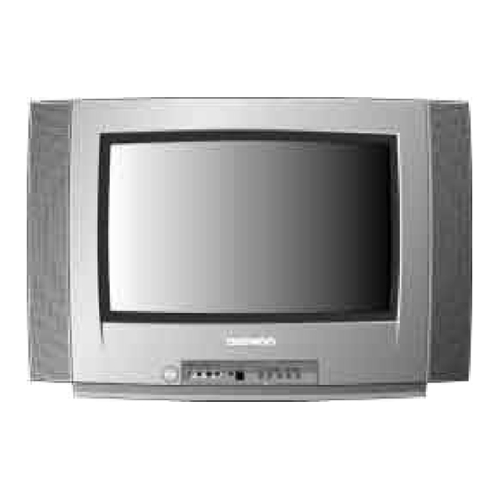
- Page 1 S/M No. : TWP895BEF0 Service Manual Colour Television CHASSIS: WP-895 MODEL: DTP-28B1 DAEWOO ELECTRONICS CO., LTD http : //svc.dwe.co.kr AUG. 2001...
- Page 2 1- Main Features 1-1 Specifications TV standard PAL - SECAM B/G D/K, PAL I/I, SECAM L/L’ Sound system NICAM B/G, I, D/K, L, FM 2Carrier B/G, D/K Power consumption 28” 4:3, FST : 69 W approx. 28” 16:9, WIDE : 69 W approx. Sound Output P o w er 28”: 7W x 2 (at 1kHz, 60% mod, 10%THD) Speaker...
- Page 3 Specification matrix CHASSIS NAME WP895 VCT VERSION 3834 SOFTWARE VERSION REMOTE CONTROL R46G22 PCB SERIAL NUMBER 4859805093 TUBE 16:09 SVHS3 "PICTURE IMPROVE- MENTS, COMB FILTER, HORIZONTAL SCALER" TELETEXT SPLIT SCREEN FORMATS AVAILABLE IN AUTO / 4:3 / 14:9 / ZOOM 14:9 / VIDEO MODE ZOOM 16:9 / FULL SCREEN AV2 MONITOR OUTPUT...
-
Page 4: Pin Euro-Scart
21 Pin EURO-SCART 1 : Signal Description Matching value Audio Output Right 0.5 Vrms, Impedance < 1 , ( RF 54% Mod ) Audio Input Right 0.5 Vrms, Impedance > 10 Audio Output Left 0.5 Vrms, Impedance < 1 , ( RF 54% Mod ) Audio Earth Blue Earth Audio Input Left... - Page 5 Video Output 1 Vpp 3dB, Impedance 75 ( Monitor output ) - Not available for cp885 Video Input, Y In. 1 Vpp 3dB, Impedance 75 Common Earth...
-
Page 6: Frequency Table
1-2 Channel table FREQUENCY TABLE EUROPE CCIR FRANCE GB(IRELAND) EAST OIRT 46.25 47.75 49.75 48.25 55.75 (L’) 53.75 59.25 55.25 60.5 (L’) 61.75 77.25 62.25 63.75 (L’) 175.25 85.25 175.25 176.00 183.25 93.25 182.25 184.00 191.25 175.25 189.25 192.00 199.25 183.25 196.25 200.00... - Page 7 EUROPE CCIR FRANCE GB(IRELAND) EAST OIRT 639.25 639.25 639.25 639.25 647.25 647.25 647.25 647.25 655.25 655.25 655.25 655.25 663.25 663.25 663.25 663.25 671.25 671.25 671.25 671.25 679.25 679.25 679.25 679.25 687.25 687.25 687.25 687.25 695.25 695.25 695.25 695.25 703.25 703.25 703.25 703.25 711.25...
- Page 8 EUROPE CCIR FRANCE GB(IRELAND) EAST OIRT 168.25 212.75 168.25 231.25 224.75 231.25 238.25 236.75 238.25 245.25 248.75 255.25 245.25 252.25 260.75 263.25 252.25 259.25 272.75 271.25 259.25 266.25 284.75 279.25 266.25 273.25 296.75 287.25 273.25 280.25 136.00 295.25 280.25 287.25 160.00 303.25 287.25...
- Page 9 1-3 A TSS sorting method The TV set sweeps all the TV bands from beginning of VHF to end of UHF. The TV controlling softw are for each program checks if a VPS CNI code is transmitted ( this system e xists for German, Swiss and Austrian transmissions). If no VPS CNI code is found , then the system check if a CNI code is transmitted as part of the teletext transmission ( Packet 8/30 format 1 ).
- Page 10 The sor ting order within group II, III, and IV is based on the channel frequency. The Pro gram with the lo west frequency is allocated the first rank in its group, and so f orth until the last program of the group which has the highest fr equency.
-
Page 11: X-Ray Radiation Precaution
2 - Safety instruction WARNING: Only competent service personnel may carry out work involving the testing or repair of this equipment. X-RAY RADIATION PRECAUTION 1. Excessive high voltage can produce potentially hazardous X-RAY RADIATION. To avoid such hazards, the high voltage must not exceed the specified limit. - Page 12 3 - Alignment instructions 3-1 Microcontroller con figuration : Service mode To switch the TV set into service mode please see instruction below. 1 - Select pr. number 91 2 - Adjust sharpness to minimum and exit all menu. 3 - Quickly press the key sequence : RED - GREEN - menu To software version is displayed beside the word Service, e.g.
- Page 13 3-3 Microcontroller con figuration : Option bits These option bits are availa ble from Service mode. First find the OPTION control, and then use keys 0...7 on the remote keypad to control bits 0 to 7 respect ively. The table below shows the options availa ble ; Tuner options TOP text FASTEXT...
- Page 14 3-4-6- Horizontal picture centring Adjust HOR CEN(Horizontal center) to have the picture in the center of the screen. 3-4-7- Eau/West comection Adjust the PARABOLA, HOR WIDTH, CORNER, HOR PARAL, EW TRAPEZ , H BOW, to compensate for geometrical distorrin, HOR PARAL H BOW For HOR WIDTH, adjust for 91% overscan.
- Page 15 CORNER EW TRAPEZ 3-4-8- AGC - Adjust the antenna signal level at 70 dB V 2 - Tune a colour bar pattern. - Find the “AGC” item in service mode. - Adjust AGC volume ( RB10 ) to bring the cursor to central position : 32. - 15 -...
- Page 16 4 - IC description 4-1 VCT383XA TV signal processor - Teletext decoder with embedded 8 bit - Controller. 4-1-1- Block diagram of the VCT 4-1-2- TV-signal Processor • Four composite video inputs, two S-VHS inputs • Analogue YC r C b input •...
- Page 17 • Horizontal scaling ( 0.25 to 4 ) • Panoramavision • Black-level expander • Dynamic peaking • Soft limiter (gamma correction) • Colour transient improvement • Programmable RGB matrix • Analogue RGB/Fastblank input • Half-contrast switch • Picture frame generator •...
- Page 18 • High-level command language • FLOF (Fastext), and TOP support • 10 pages memory on chip (10kB) 4-1-5- Display OSD Features • 3kB OSD RAM on chip • WST level 1.5 compliant • WST level 2 parallel attributes • 32 foreground/background colours •...
-
Page 19: Short Description
• Inventory of transmitted Teletext pages stored in the Page Table • Signal quality detector for WST data • Comprehensive Teletext language coverage • Full Field Vertical Blanking Interval (VBI) data capture of WST data 4-1-10- TV processor version and -Controller capacity IC version VCT 3832A VCT 3834A... - Page 20 PSDIP Pin Name Short Description Type 64-pin GNDAF SUPPLY Ground, Analog Front-end VSUPAF SUPPLY Supply Voltage, Analog Front-end CBIN Analog Component Cb Input CIN1 Analog Chroma 1 Input CIN2/CRIN Analog Chroma 2 Input / Analog Component Cr Input VIN1 Analog Video 1 Input VIN2 Analog Video 2 Input VIN3...
- Page 21 Power S/B 5V MUTE MOD SW SECAM L’ AFC/RES RESET XTAL in SC1 SW OSC GND SC2 SW Vout S/B 3.3V SGND Cb in C in XREF Cr in IF-IN SC1-IN SC2-IN B out RCA VIN G out TEST R out H out SVM out 3.3 V...
- Page 22 4-2 MSP341x Multistandard Sound Processor The MSP 341x is designed as a single-chip Multistandard Sound Processor for applications in analogue and digital TV sets, video recorders, and PC cards. The MSP3411 has all functions of MSP3410 with the addition of a virtual surround sound feature. A Surround sound affect can be r produced with two loudspeakers.
-
Page 23: Nicam Plus Fm/Am-Mono
- high deviation FM-mono mode (max. deviation: approx. ±360 kHz) 4-2-1-2 DSP-Section (Audio Baseband Processing) - flexible selection of audio sources to be processed - performance of terrestrial de-emphasise systems (FM, NICAM) - digitally performed FM-identification decoding and de-matrixing - digital baseband processing: volume, bass, treble - simple controlling of volume, bass, treble 4-2-1-3 Analogue Section - two selectable analogue pairs of audio baseband input (= two SCART inputs) input level: <2 V RMS,... - Page 24 TV standards Position of sound Sound modulation Color system Country system carrier (MHz) 5.5 / 5.7421875 FM Stereo Germany 5.5 / 5.85 FM-Mono / NICAM Scandinavia, Spain 6.5 / 5.85 AM-Mono / NICAM SECAM-L France 6.0 / 6.552 FM-Mono / NICAM 6.5 / 6.2578125 D/K1 FM Stereo SECAM-East...
- Page 25 Pin No. Pin Name Type Short description In / Out Test pin Test pin Not Connected Test pin Test pin Test pin DVSUP Digital power supply +5V DVSS Digital Ground Not Connected Not Connected Not Connected Not Connected RESETQ Power-On-reset Not Connected Not Connected VREF2...
- Page 26 Pin No. Pin Name Type Short description ANA_IN1- IF common Not Connected TESTEN Test pin XTAL_IN Crystal oscillator XTAL_OUT Crystal oscillator Test pin 4-3 TDA 4470-Multistandard Video-IF and Quasi Parallel Sound Processor 4-3-1- Description The TDA 4470 is an integrated bipolar circuit for multi-standard video/sound IF (VIF/SIF) signal processing in TV/VCR and multimedia applications.
-
Page 27: Block Diagram
Symbol Function AFC switch 20, 21 VCO circuit AFC output Supply voltage Intercarrier output O, FM AF output-AM sound O, AM Offset compensation COMP 27, 28 SIF2 input (symmetrical) i,SIF2 4-3-4 Block diagram l' switch Loop Offset filter comp. (optional) Control FPLL phase shift... - Page 28 4-4 TDA894xJ Stereo Audio Amplif i er The TDA8944J( TDA 8946J) is a dual-channel audio po wer amplifier with an output power of 2 x 7W (2 X 15W) at an 8 load and a 12V supply. The circuit contains two Bridges Tied Load(BTL) amplif i ers with an all-NPN output stage and standby/mute logic.
- Page 29 Block diagram TDA8944J - 29 -...
- Page 30 4-5 TDA835xJ Vertical Amplifier The TDA835xJ are power circuit for use in 90 and 110 colour deflection systems for field frequencies of 25 to 200Hz and 16/9 picture tubes. The circuit provides a DC driven vertical deflection output circuit, operating as a highly efficient class G system. Due to the full bridge output circuit the deflection coils can be DC coupled.
- Page 31 4-5-2 TDA8358J An East-West output stage is provided that is able to sink current from the diode modulator circuit. Features : - Few external components - Highly efficient fully DC-coupled vertical output bridge circuit - Short rise and fall time of the vertical flyback switch - Guard circuit - Temperature (thermal) protection - High EMC because of common mode inputs...
- Page 32 - 32-...
- Page 33 4-6 TDA6107Q The TDA6107Q includes three video output amplifiers in one plastic DIL-Bent-SIL 9-pin medium power package, using high voltage DMOS technology, and is intended to drive the three cathodes of a colour CRT directly. To obtain maximum performance, the amplifier should be used with black-current control. Features - Typical bandwidth of 5.5 MHz for an output signal of 60 Vpp - High slew rate of 900V/ s...
- Page 34 Block diagram TDA6107Q - 34 -...
- Page 35 4-6 24C16 - 16 Kb EEPROM features : - 16 Kbit serial I2C bus EEPROM - Single supply voltage : 4.5 V to 5.5 V - 1 Million Erase/Write cycles (minimum) - 40 year data retention (minimum) Pin description Pin No. Name Description 1, 2, 3...
- Page 36 4-8 STR - F6653 4-8-1 General description The STR-F6653 is an hybrid IC with a build-in MOSFET and control IC, designed for flyback converter type switch mode power supply applications. 4-8-2 Features - Small SIP fully isolated molded 5 pins package - Many protection functions : * Pulse-by-pulse overcurrent protection (OCP) * Overvoltage protection with latch mode (OVP)
- Page 37 4-8-4 Pins description name symbol description Overcurrent / feedback O.C.P./ F.B. Input of over current detection signal and feedback signal Source MOSFET source Drain MOSFET drain Supply Input of power supply for control circuit Ground Ground 4-8-5 Control part electrical characteristics IC PIN RATING SYMBOL...
- Page 38 4-7-6 MOSFET electrical characteristics IC PINS RATING DESCRIPTION SYMBOL UNIT NUMBER MIN. TYPE Drain-to-source break voltage Drain leakage current On-resistance (on) 1.95 Switching time noec Thermal resistance 0.95 - 38 -...
- Page 39 5 - Circuit description 5-1 Block diagram - 39 -...
- Page 40 5-2 IF section 5-2-1 Block diagram 5-2-2 Vision IF Amplifier The video IF signal (VIF) is fed through a SAW filter to the differential input (Pin 6-7) of the VIF amplifier. This amplifier consists of three AC-coupled amplifier stages. Each differential amplifier is gain controlled by the automatic gain control circuit (VIF-AGC).
-
Page 41: Tuner-And Vif-Agc
SAW filters Ref. Standard Features K3953M B/G - D/K - I - L/L’ - IF filter for video application - TV IF filter with Nyquist slopes at 33.9 MHz and 38.9 MHz - Constant group delay K9650M B/G - D/K - I - L/L’ - IF filter for audio application - TV IF audio filter with two channels - Channel 1 (L’... - Page 42 5-2-5 Video Demodulation and Amplifier The video IF signal, which is applied from the gain controlled IF amplifier, is multiplied with the in-phase component of the VCO signal. The video demodulator is designed for low distortion and large bandwidth. The demodulator output signal passes an integrated low pass filter for attenuation of the residual vision carrier and is fed to the video amplifier.
-
Page 43: Digitally Controlled Clock Oscillator
5-3 Video - VCT description 5-3-1 Introduction The VCT 38xxA includes complete video, display, and deflection processing. All processing is done digitally, the video front-end and video back-end are interfacing to the analogue world. Most functions can be controlled by software via I 2 C bus slave interface. 5-3-2 Video Front-end This block provides the analogue interfaces to all video inputs and mainly carries out analogue-to-digital conversion for the following digital video processing. -
Page 44: Adaptive Comb Filter (Vct3834A Only)
5-3-8 Adaptive Comb Filter (VCT3834A only) The adaptive comb filter is used for high-quality luminance/chrominance separation for PAL or NTSC signals. The comb filter improves the luminance resolution (bandwidth) and reduces interferences like cross-luminance and cross-color artefacts. The adaptive algorithm can eliminate most of the mentioned errors without introducing new artefacts or noise. - Page 45 5-3-11 Video Sync Processing To extract the sync information from the video signal, a linear phase low-pass filter eliminates all noise and video contents above 1 MHz. The sync is separated by a slicer; the sync phase is measured. A variable window can be selected to improve the noise immunity of the slicer.
- Page 46 5-3-15 CRT Measurement and Control The display processor is equipped with an 8-bit ADC for all measuring purposes. The ADC is connected to the SENSE input pin. Cutoff and white-drive current measurement are carried out during the vertical blanking interval. 5-3-16 Average Beam Current Limiter The average beam current limiter (BCL) uses the SENSE input for the beam current measurement.
-
Page 47: Eht Compensation
5-3-20 EHT Compensation The vertical waveform can be scaled according to the average beam current. This is used to compensate the effects of electric high-tension changes due to beam current variations. EHT compensation for East/West deflection is done with an offset corresponding to the average beam current. 5-3-21 Reset Function Reset of all VDP functions is performed by the RESQ pin. - Page 48 5-4-3 - Controller I/O pin configuration and function There exist different kinds of ports. The universal ports serve as digital I/O and have additional special input and output functions. A subset of the universal ports serves as input for the analogue-to-digital converter. - Controller I/O pin configuration and function table configuration name...
- Page 49 23, in each frame. This is bi-phase encoded using a clock frequency of 5 MHz. In total, 14 data bits are available, in 4 groups. Group 1 contains the codes for the received format. The mode chosen is defined by the following table. In effect the default mode is full screen. The table below gives a summary of the FORMAT modes available (for WP895 and WP895F), and their given properties.
- Page 50 The following schematic, illustrates the logic of control for the two SCART connectors. The terms used in the schematic are described below ; 1. AUTO represents a situation where the television has self-selected its picture source. This could be when the SCART SLOW SWITCHING pin has gone to a high state, and the AV 1 input is selected without the intervention of the user.
- Page 51 can always be overridden by the user after the event. Each line on the diagram, with its associated text, represents the exact conditions under which the change of state will occur. Sometimes this will be accompanied by another action which will be automatically performed by the television, being to either ENABLE or DISABLE F/SW 1.
- Page 52 OSD Language C Teletext Language Mapping Teletext Language English English Latin English, French, German German Latin German, Italian, Swedish/Finnish Swedish/Finnish Latin Spanish, Dutch, Italian Italian Latin Danish, Finnish, French French Latin Norwegian, Spanish Spanish Latin Swedish, Greek Turkish Turkish Latin English Greek Greek/Cyrillic...
-
Page 53: Nicam Decoder
5-6-4 NICAM decoder In case of NICAM - mode, the phase samples are decoded according the DQPSK - coding scheme. The output of this block contains the original NICAM bitstream. 5-6-5 DSP section All audio baseband functions are performed by digital signal processing (DSP). The DSP section controls the source and output selection, and the signals processing. -
Page 54: Flyback Voltage
5-7-2 Mode selection The TDA894xJ has several functional modes, which can be selected by applying the proper DC voltage to pin MODE. Mute : In this mode the amplifier is DC biased but not operational (no audio output). This allows the input coupling capacitors to be charged to avoid pop-noise. - Page 55 5-9 Power supply (STR F6654) 5-9-1 STR-F6654 general description The STR-F6654 is an hybrid IC with a build-in MOSFET and control IC, designed for flyback converter type switch mode power supply applications. 5-9-2 Power supply primary part operations An oscillator generates pulses signals which turn on and off a MOSFET transistor. 5-9-2-1 Start-up circuit : V The start-up circuit is used to start and stop the operation of the control IC, by detecting a voltage appearing at V pin (pin 4).
- Page 56 When the power switch is pushed on, V increases slowly. During this time, C806 is charged through R802. As soon as V reaches 16V, the STR-F6654 control circuit starts operating. Then, V is obtained by smoothing the winding voltage which appears between pin6 and pin7 of the SMPS transformer. As this winding voltage does not increase to the set voltage immediately after the control circuit starts operating, V starts dropping.
-
Page 57: Str-F6654 Oscillating Operation
5-9-2-2 STR-F6654 oscillating operation - 57 -... - Page 58 When the MOSFET is ON, the STR-F6654 internal capacitor C1 is charged at the constant voltage 6.5V. At the same time, the voltage at pin 1 (OCP / FB) increases with the same waveform as the MOSFET drain current. When the pin 1 voltage reaches the threshold voltage V = 0.73V, the STR-F6654 internal comparator 1 starts operating.
- Page 59 5-10 TV start-up, TV normal run and stand by mode operations 5-10-1 TV start-up operations * Schematic diagram for start-up operations * TV start-up and microcontroller initialisation - When SW801 power switch is pushed, main AC voltage is applied to T801 transformer (after rectification by D801... D804 diodes).
- Page 60 . If the TV set was on normal run mode before switching off, the microcontroller delivers horizontal drive voltage at pin 24 and picture appears on screen. . If the TV set was on stand-by mode before switching off, the microcontroller switches TV set to stand-by mode, decreasing power pin voltage (pin 1).
- Page 61 On normal run mode, I501 microcontroller pin 1 (power) is set to high • So, I810 controlled rectifier is not conducting - Q809 is conducting. So, Q808 is not conducting and Q807 is conducting - So, Q807 collector is connected to the ground and I810 controlled rectifier gate pin is set to low (no conducting) •...
- Page 62 * power supply functioning during TV set normal run mode - I801 transmits controlled pulses to T801 which generates DC voltages after rectifications by secondary part diodes and electro capacitors (by example by D820 and C813 on 143V supply voltage line). - 8V, 5V, 3.3V supply voltage lines have stabilized voltages obtained by I820, I822, I823 voltage regulators.
- Page 63 I810 CONDUCTING controlled rectifier I823 3.3V R E G U L A T O R D821 C840 HIGH C841 AROUND AROUND 3.3Vdc 6V dc D825 T801 SM PS TRA N S R810 R713 I810 C O N T R O L L E D RECTIFIER I703 IR SW I T C H I N G...
- Page 64 I810 CONTROLLED RECTIFIER 6V DC HIGH R829 R830 R820 C830 HIGH Q807 Q808 HIGH POWER Q809 Fig : I810 controlled rectifier switching circuit * TV set stand-by mode operations - On stand-by mode, I501 microcontroller pin 1 (power) is set to low. - So, Q809 collector is set to high.
-
Page 65: Service Parts List
6. Service Parts List CAUTION “ ” Parts recommended for stock. “ ® ” Safety critical componen, Replace only with genuine Deawoo safety parts. PART CODE PART NAME DESCRIPTION REMARK LOC PART CODE PART NAME DECSCRIPTION REMARK M211 4852158911 COVER BACK HIPS GY PW001 4857417700 TERM CLAMP... - Page 66 PART CODE PART NAME DESCRIPTION REMARK LOC PART CODE PART NAME DECSCRIPTION REMARK G900 4SG0D00103 SPARK GAP S-23 900V-1.5KV Q401B 7174300811 SCREW TAPPTITE TT2 RND 3X8 MFZN I101 1TDA4470M- IC IF TDA4470-M R398 RD-2Z109J- R CARBON FILM 1/2 1 OHM J ®...
- Page 67 PART CODE PART NAME DESCRIPTION REMARK LOC PART CODE PART NAME DECSCRIPTION REMARK C623 CEXF1H109V C ELECTRO 50V RSS 1MF (5X11) TP C156 CBXF1H104Z C CERA SEMI 50V F 0.1MF Z (TAPPING) C624 CEXF1H109V C ELECTRO 50V RSS 1MF (5X11) TP C157 CEXF1H100V C ELECTRO...
- Page 68 LOC PART CODE PART NAME DECSCRIPTION REMARK PART CODE PART NAME DESCRIPTION REMARK Q334 T2SC5343Y- 2SC5343Y C161 CZSL1H220J C CERA 50V SL 22PF J (AXIAL) Q402 T2SD1207T- 2SD1207-T (TAPPING) C163 CCZF1H103Z C CERA 50V F 0.01MF Z Q510 T2SC5343Y- 2SC5343Y C500 CCZF1H103Z C CERA...
- Page 69 LOC PART CODE PART NAME DECSCRIPTION REMARK PART CODE PART NAME DESCRIPTION REMARK CA20 CCZB1H222K C CERA 50V B 2200PF K (AXIAL) D840 D1N4148— DIODE 1N4148 (TAPPING) CCZB1H101K C CERA 50V B 100PF K (AXIAL) D841 D1N4148— DIODE 1N4148 (TAPPING) CCZB1H102K C CERA 50V B 1000PF K (AXIAL)
- Page 70 PART CODE PART NAME DESCRIPTION REMARK LOC PART CODE PART NAME DECSCRIPTION REMARK J072 85801065GY WIRE COPPER AWG22 1/0.65 TIN COATING J891 85801065GY WIRE COPPER AWG22 1/0.65 TIN COATING J073 85801065GY WIRE COPPER AWG22 1/0.65 TIN COATING J896 85801065GY WIRE COPPER AWG22 1/0.65 TIN COATING J075 85801065GY...
- Page 71 LOC PART CODE PART NAME DECSCRIPTION REMARK PART CODE PART NAME DESCRIPTION REMARK R162 RD-AZ153J- R CARBON FILM 1/6 15K OHM J R540 RD-AZ101J- R CARBON FILM 1/6 100 OHM J R163 RD-AZ752J- R CARBON FILM 1/6 7.5K OHM J R541 RD-AZ122J- R CARBON FILM...
- Page 72 PART CODE PART NAME DESCRIPTION REMARK LOC PART CODE PART NAME DECSCRIPTION REMARK R913 RD-AZ101J- R CARBON FILM 1/6 100 OHM J R621 RD-AZ102J- R CARBON FILM 1/6 1K OHM J R921 RC-2Z102K- R CARBON COMP 1/2 1K OHM K R622 RD-AZ102J- R CARBON FILM...
-
Page 73: Exploded View
7. Exploded View 7-5 DTP-28B1 - 73 -... -
Page 74: Printed Circuit Board
PRINTED CIRCUIT BOARD PCB MAIN...
Need help?
Do you have a question about the DTP-28B1 and is the answer not in the manual?
Questions and answers