Table of Contents
Advertisement
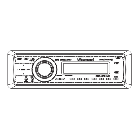
MULTI-CD CONTROL HIGH POWER CD/MP3/WMA/AAC PLAYER WITH FM/AM TUNER
DEH-P5850MP
MULTI-CD CONTROL HIGH POWER CD/MP3/WMA PLAYER WITH FM/AM TUNER
DEH-P5850MPH
This service manual should be used together with the following manual(s):
Model No.
Order No.
CX-3164
CRT3583
For details, refer to "Important Check Points for Good Servicing".
PIONEER CORPORATION
PIONEER ELECTRONICS (USA) INC. P.O. Box 1760, Long Beach, CA 90801-1760, U.S.A.
PIONEER EUROPE NV Haven 1087, Keetberglaan 1, 9120 Melsele, Belgium
PIONEER ELECTRONICS ASIACENTRE PTE. LTD. 253 Alexandra Road, #04-01, Singapore 159936
PIONEER CORPORATION 2005
Mech.Module
S10.5COMP1
CD Mech. Module : Circuit Descriptions, Mech. Descriptions, Disassembly
4-1, Meguro 1-chome, Meguro-ku, Tokyo 153-8654, Japan
DEH-P5850MP/XN/ES
/XN/GS
Remarks
ORDER NO.
CRT3565
/XN/ES
K-ZZA.NOV. 2005 Printed in Japan
Advertisement
Table of Contents

Subscribe to Our Youtube Channel
Related Manuals for Pioneer DEH-P6880MP


Summary of Contents for Pioneer DEH-P6880MP
- Page 1 PIONEER CORPORATION 4-1, Meguro 1-chome, Meguro-ku, Tokyo 153-8654, Japan PIONEER ELECTRONICS (USA) INC. P.O. Box 1760, Long Beach, CA 90801-1760, U.S.A. PIONEER EUROPE NV Haven 1087, Keetberglaan 1, 9120 Melsele, Belgium PIONEER ELECTRONICS ASIACENTRE PTE. LTD. 253 Alexandra Road, #04-01, Singapore 159936 PIONEER CORPORATION 2005 K-ZZA.NOV.
-
Page 2: Safety Information
SAFETY INFORMATION This service manual is intended for qualified service technicians; it is not meant for the casual do-it-yourselfer. Qualified technicians have the necessary test equipment and tools, and have been trained to properly and safely repair complex products such as those covered by this manual. Improperly performed repairs can adversely affect the safety and reliability of the product and may void the warranty. - Page 3 [Important Check Points for Good Servicing] In this manual, procedures that must be performed during repairs are marked with the below symbol. Please be sure to confirm and follow these procedures. 1. Product safety Please conform to product regulations (such as safety and radiation regulations), and maintain a safe servicing environment by following the safety instructions described in this manual.
-
Page 4: Table Of Contents
CONTENTS SAFETY INFORMATION ............................. 2 1. SPECIFICATIONS ............................5 2. EXPLODED VIEWS AND PARTS LIST ......................7 2.1 PACKING ..............................7 2.2 EXTERIOR..............................8 2.3 CD MECHANISM MODULE........................10 3. BLOCK DIAGRAM AND SCHEMATIC DIAGRAM ..................12 3.1 BLOCK DIAGRAM ........................... 12 3.2 OVERALL CONNECTION DIAGRAM(GUIDE PAGE)................ -
Page 5: Specifications
1. SPECIFICATIONS DEH-P5850MP/XN/ES... - Page 6 DEH-P5850MP/XN/ES...
-
Page 7: Exploded Views And Parts List
2. EXPLODED VIEWS AND PARTS LIST OTES : • Parts marked by " * " are generally unavailable because they are not in our Master Spare Parts List. • The > mark found on some component parts indicates the importance of the safety factor of the part. Therefore, when replacing, be sure to use parts of identical designation. -
Page 8: Exterior
2.2 EXTERIOR DEH-P5850MP/XN/ES... - Page 9 EXTERIOR SECTION PARTS LIST Mark No. Description Part No. Mark No. Description Part No. Connector(CN1901) CKS5207 Screw ASZ26P050FTC Screw BMZ30P040FTB Cushion CNM6633 Screw BSZ26P060FTC Spacer CNM7697 Screw BSZ30P060FTC Spacer CNM7698 Screw BSZ30P200FTC Holder CNV6910 OEL Unit MXS8221 Case CNB2793 Holder CNC8659 Holder XNC7006...
-
Page 10: Cd Mechanism Module
2.3 CD MECHANISM MODULE DEH-P5850MP/XN/ES... - Page 11 CD MECHANISM MODULE SECTION PARTS LIST Mark No. Description Part No. Mark No. Description Part No. Rack CNV8342 CD Core Unit(S10.5COMP1) CWX3176 Connector(CN101) CKS4182 Roller CNV8343 Connector(CN901) CKS5284 Holder CNV8344 Screw BMZ20P025FTC CNV8345 Screw BSZ20P040FTC Guide CNV8347 CNV8348 Screw(M2 x 3) CBA1511 Screw(M2 x 4) CBA1835...
-
Page 12: Block Diagram And Schematic Diagram
3. BLOCK DIAGRAM AND SCHEMATIC DIAGRAM 3.1 BLOCK DIAGRAM TUNER AMP ASSY 10 9 8 18 19 20 21 FM/AM TUNER UNIT IC 5 IC 3 EEPROM 3.3V 5.0V ANTENNA CN401 AM ANT FMRF IC 2 2.5V IC 1 FM ANT 3.3V FMRF MIXER, IF AMP... - Page 13 DEH-P5850MP/XN/ES only RESET CN351 MUTE IC602 REAR L S-80835CNUA-B8U Q351 NON-FAD/SW L Q353 CN352 TUNPCE2 FRONT L TUNPCE1 TUNPDI TUNPDI TUNPDO TUNPDO Q352 TUNPCK VDD REGULATOR TUNPCK Q911 Q912 SYSTEM CONTROLLER IC 601(1/2) DALMON PEG146A CN901 BACKUP SENSE B.UP FUSE B.UP BSENS BACK UP...
-
Page 14: Overall Connection Diagram(Guide Page)
3.2 OVERALL CONNECTION DIAGRAM(GUIDE PAGE) Note: When ordering service parts, be sure to refer to " EXPLODED VIEWS AND PARTS LIST" or "ELECTRICAL PARTS LIST". Large size SCH diagram IP-Bus: 2.20dBs FM, AM:-24.00dBs Guide page Detailed page FM,AM:-0.9 CD:10.01d IP-Bus:9.3 EJECT CSG1135:ES,CSG1112:CN,GS CD:0.36dBs... - Page 15 TUNER AMP ASSY NOTE : The > mark found on some component parts indicates Symbol indicates a resistor. No differentiation is made between chip resistors and the importance of the safety factor of the part. discrete resistors. Therefore, when replacing, be sure to use parts of Symbol indicates a capacitor.
- Page 16 DEH-P5850MP/XN/ES...
- Page 17 DEH-P5850MP/XN/ES...
- Page 18 DEH-P5850MP/XN/ES...
- Page 19 DEH-P5850MP/XN/ES...
-
Page 20: Keyboard Unit
3.3 KEYBOARD UNIT CN1951 DEH-P5850MP/XN/ES... - Page 21 KEYBOARD UNIT KEY/OEL CONTROLLER OEL UNIT DEH-P5850MP/XN/ES...
-
Page 22: Cd Mechanism Module(Guide Page)
3.4 CD MECHANISM MODULE(GUIDE PAGE) PICKUP UNIT(P10.5)(SERVICE) SWITCHES: CD CORE UNIT(S10.5COMP1) S901:HOME SWITCH..ON-OFF S903:DSCSNS SWITCH..ON-OFF S904:12EJ SWITCH.....ON-OFF S905:8EJ SWITCH....ON-OFF The underlined indicates the switch position. CD DRIVER M1 CXC6742 SPINDLE MOTOR M2 CXC4026 LOADING/CARRIAGE MOTOR DEH-P5850MP/XN/ES... - Page 23 SIGNAL LINE NOTE : Decimal points for resistor and capacitor fixed values FOCUS SERVO LINE are expressed as : TRACKING SERVO LINE ← ← CARRIAGE SERVO LINE 0.022 R022 SPINDLE SERVO LINE CD CORE UNIT(S10.5COMP1) + 3.3 V REGULATOR CD3VON(MCKRQ) SRAMLEVEL2 ADENA SRAMLEVEL1...
- Page 24 DEH-P5850MP/XN/ES...
- Page 25 DEH-P5850MP/XN/ES...
- Page 26 DEH-P5850MP/XN/ES...
- Page 27 DEH-P5850MP/XN/ES...
- Page 28 - Waveforms Note : 1. The encircled numbers denote measuring points in the circuit diagram. 2. Reference voltage REFO1(1.65 V) 1 DSCSNS 1 DSCSNS 1 DSCSNS 5 V/div 500 ms/div 5 V/div 500 ms/div 5 V/div 500 ms/div 2 8SNS 4 CLCONT 2 8SNS 5 V/div...
- Page 29 500 µs/div 9 FIN ! TE $ RFAGC 500 mV/div 200 ms/div 500 mV/div 2 ms/div 1 V/div @ FE $ RFAGC ! TE 500 mV/div 500 mV/div 500 mV/div 8 TIN 500 mV/div Focus Search waveform Track Open waveform 1 Track Jump waveform Ref.: Ref.:...
- Page 30 500 µs/div 6 SIN $ RFAGC 1 V/div 500 ms/div 1 V/div 7 CIN 8 TIN 500 mV/div 1 V/div 8 TIN ! TE 500 mV/div 1 V/div 9 FIN 1 V/div CD-ROM → CD-DA mode change(Band key) Black dot(800 µm) during play Ref.: Ref.: REFO...
- Page 31 DEH-P5850MP/XN/ES...
-
Page 32: Pcb Connection Diagram
4. PCB CONNECTION DIAGRAM 4.1 TUNER AMP ASSY NOTE FOR PCB DIAGRAMS TUNER AMP ASSY 1.The parts mounted on this PCB CORD ASSY include all necessary parts for several destination. For further information for WIRED respective destinations, be sure REMOTE IP-BUS to check with the schematic dia- gram. - Page 33 SIDE A REAR OUT ANTENNA JACK CN651 CN1950 FRONT DEH-P5850MP/XN/ES...
- Page 34 TUNER AMP ASSY TESTIN DEH-P5850MP/XN/ES...
- Page 35 SIDE B DEH-P5850MP/XN/ES...
-
Page 36: Keyboard Unit
4.2 KEYBOARD UNIT KEYBOARD UNIT AUDIO FUNCTION S1901 SOURCE/VOL DISPLAY BAND KEYBOARD UNIT DEH-P5850MP/XN/ES... - Page 37 SIDE A PAUSE CLOCK SIDE B CN1951 DEH-P5850MP/XN/ES...
-
Page 38: Cd Core Unit(S10.5Comp1)
4.3 CD CORE UNIT(S10.5COMP1) SIDE A CD CORE UNIT(S10.5COMP1) PICKUP UNIT(P10.5)(SERVICE) CN651 REFO1 HOME CN901 LOADING /CARRIAGE MOTOR SPINDLE MOTOR IC203 IC301 DEH-P5850MP/XN/ES... - Page 39 SIDE B CD CORE UNIT(S10.5COMP1) 12EJ DSCSNS DEH-P5850MP/XN/ES...
-
Page 40: Panel Unit
4.4 PANEL UNIT SIDE A PANEL UNIT CN1901 EJECT SIDE B PANEL UNIT CN801 DEH-P5850MP/XN/ES... -
Page 41: Electrical Parts List
5. ELECTRICAL PARTS LIST NOTE: Parts whose parts numbers are omitted are subject to being not supplied. • The part numbers shown below indicate chip components. • Chip Resistor RS1/_S___J,RS1/__S___J Chip Capacitor (except for CQS..) CKS.., CCS.., CSZS..The > mark found on some component parts indicatesthe importance of the safety factor of the part. •... - Page 42 Circuit Symbol and No. Part No. Circuit Symbol and No. Part No. L 101 (A,32,80) Inductor LAU2R2K R 355 (B,157,120) RS1/16S821J L 201 (A,74,80) Ferri-Inductor LAU4R7K R 356 (B,144,128) RS1/16S821J L 401 (A,156,50) Inductor LAU1R0K R 357 (B,133,112) (ES) RS1/16S223J L 402 (A,148,91) Inductor LAU1R0K...
- Page 43 Circuit Symbol and No. Part No. Circuit Symbol and No. Part No. R 817 (B,103,28) RS1/16S473J C 209 (A,67,96) CEJQ1R0M50 R 818 (B,129,26) RS1/16S104J R 820 (A,105,34) RS1/16S0R0J C 210 (A,60,96) CEJQ1R0M50 R 821 (A,53,22) RD1/4PU391J C 211 (A,68,91) CEJQ1R0M50 C 212 (A,60,86) CEJQ1R0M50...
- Page 44 Circuit Symbol and No. Part No. Circuit Symbol and No. Part No. C 756 (B,88,86) CKSRYB104K16 S 1912 (A,157,16) Push Switch CSG1135 S 1913 (A,29,10) Push Switch CSG1135 C 803 (A,97,11) CKSRYB104K16 S 1914 (A,88,6) Push Switch CSG1175 C 821 (B,76,14) CKSRYB473K50 C 822...
- Page 45 Circuit Symbol and No. Part No. Circuit Symbol and No. Part No. R 1996 (B,117,16) RS1/16S222J S 1908 (A,14,15) Switch CSG1107 R 1997 (B,113,16) RS1/16S222J S 1909 (A,68,6) Push Switch CSG1112 R 1998 (A,80,18) RS1/16S102J R 1999 (A,78,17) RS1/16S102J S 1910 (A,18,9) Push Switch CSG1112 S 1911...
- Page 46 Circuit Symbol and No. Part No. Circuit Symbol and No. Part No. R 1992 (B,108,24) RS1/16S101J IC 201 (B,39,70) IC UPD63763CGJ R 1993 (B,94,29) RS1/16S101J IC 203 (A,12,16) IC NJM2886DL3-33 R 1994 (B,94,32) RS1/16S101J IC 301 (A,28,18) IC BA5835FP IC 701 (A,32,48) IC PE5505A R 1995...
- Page 47 Circuit Symbol and No. Part No. R 906 (B,20,36) RS1/16SS221J R 907 (B,16,62) RS1/16SS0R0J R 908 (B,16,64) RS1/16SS0R0J R 911 (B,20,32) RS1/16SS0R0J CAPACITORS C 103 (B,57,83) CEVW101M16 C 108 (A,47,66) CKSSYB104K10 C 201 (B,46,56) CKSSYB102K50 C 202 (B,47,58) CKSSYB104K10 C 204 (B,35,48) CEVW220M6R3 C 205...
-
Page 48: Adjustment
6. ADJUSTMENT 6.1 CD ADJUSTMENT 1) Cautions on adjustments 2) Test mode • In this product the single voltage (3.3V) is used for the This mode is used to adjust the CD mechanism module. regulator. The reference voltage is the REFO1 (1.65V) •... - Page 49 - Flow Chart [Key] [4] + [6] + Reset or [4] + [6] + BU + ACC Contents Test Mode In Display [CD] or [SOURCE] Source On [BAND] Power On Power On RF AMP SPINDLE (T.Offset is adjusted) (T.Offset is not adjusted) Gain switching Speed switching 00 00 00...
-
Page 50: Checking The Grating After Changing The Pickup Unit
6.2 CHECKING THE GRATING AFTER CHANGING THE PICKUP UNIT • Note : The grating angle of the PU unit cannot be adjusted after the PU unit is changed. The PU unit in the CD mechanism module is adjusted on the production line to match the CD mechanism module and is thus the best adjusted PU unit for the CD mechanism module. - Page 51 Ech → Xch 20mV/div, AC Grating waveform Fch → Ych 20mV/div, AC 0° 30° 45° 60° 75° 90° DEH-P5850MP/XN/ES...
-
Page 52: Error Mode
6.3 ERROR MODE - Error Messages If a CD is not operative or stopped during operation due to an error, the error mode is turned on and cause(s) of the error is indicated with a corresponding number. This arrangement is intended at reducing nonsense calls from the users and also for facilitating trouble analysis and repair work in servicing. -
Page 53: System Microcomputer Test Program
6.4 SYSTEM MICROCOMPUTER TEST PROGRAM - PCL output In the normal operation mode (with the detachable panel installed, the ACC switched ON, the standby mode cancelled), shift the TESTIN IC601 (Pin 86) terminal to H. The clock signal is output from the PCL terminal IC601 (Pin 37). The frequency of the clock signal is 468.75 kHz that is one 32th of the fundamental frequency. -
Page 54: General Information
7. GENERAL INFORMATION 7.1 DIAGNOSIS 7.1.1 DISASSEMBLY Removing the Case (not shown) 1. Remove the Case. CD Mechanism Module Removing the CD Mechanism Module (Fig.1) Remove the four screws. Disconnect the connector and then remove the CD Mechanism Module. Removing the Grille Assy (Fig.1) Remove the two screws and then remove the Grille Assy. - Page 55 - How to hold the Mechanism Unit 1. Hold the Upper and Lower Frames. 2. Do not hold the front portion of the Upper Frame, because it is not very solid. Do not squeeze this area. - Removing the Upper and Lower Frames 1.
- Page 56 - How to remove the CD Core Unit Shorting Solder 1. Apply Shorting Solder to the flexible cable of the Pickup, and disconnect it from the connector. 2. Unsolder the four leads, and loosen the Screw. 3. Remove the CD Core Unit. Caution: When assembling the CD Core Unit, assemble it with the SW in a clamped state so as not to damage it.
-
Page 57: Connector Function Description
7.1.2 CONNECTOR FUNCTION DESCRIPTION 1 0 A DEH-P5850MP/XN/ES... - Page 58 7.2 IC - Pin Functions (UPD63763CGJ) Function and Operation Pin No. Pin Name Power supply for digital circuits D.VDD Ground for 1.6 V digital circuits D1.GND reset Input of reset Address bus 12-8 from the microcomputer AB12-8 Address/data bus 7-0 to the microcomputer 9-16 AD7-0 Chip selection...
- Page 59 Function and Operation Pin No. Pin Name Output of DRAM we Output of DRAM oe(cas) oe(cas) D.GND Ground for digital circuits Input/output of DRAM data0-15 73-88 RDB0-15 Output of DRAM address0-10 89-99 RA0-10 Power supply for digital circuits D.VDD Output of focus drive PWM + Output of focus drive PWM - Output of tracking drive PWM + Output of tracking drive PWM -...
- Page 60 - Pin Functions (PE5505A) Function and Operation Pin No. Pin Name Format A power supply / Positive power supply(5V) AVREF AVSS A power supply GND testin Chip check test program starting input Not used CLAMP E power supply / Positive power supply EVDD For flash rewriting / L : flash rewriting mode FMODE...
- Page 61 Function and Operation Pin No. Pin Name Format E2PROM data input/output ROMDATA E2PROM clock output ROMCK E2PROM chip selection output ROMCS 60,61 Not used Not used CLKOUT LOCK Spindle lock input Not used 64-68 B power supply GND BVSS B power supply / Positive power supply BVDD Not used 71-75...
- Page 62 - Pin Functions (PEG203A) Function and Operation Pin No. Pin Name Format Not used ROMDT Not used Not used ROMCK romcs Not used Remote control reception External data bus width change input BYTE Processor mode change input CNVSS Not used reset Reset Radiator(10 MHz)
- Page 63 * PEG203A Format meaning C MOS Nch open drain * PD8156A HA12241FP -BUS +BUS BIAS DRIVER OUTPUT (current) RECEIVER OUTPUT R out DEH-P5850MP/XN/ES...
- Page 64 PAL007B DEH-P5850MP/XN/ES...
- Page 65 - Pin Functions (PEG146A) Function and Operation Pin No. Pin Name System power control output SYSPW KEYD Wired remote control : Key data input Not used rst@ Reset output for CD mechanism Not used External data bus width change input BYTE Processor mode change input CNVSS...
- Page 66 Function and Operation Pin No. Pin Name ROMCS ROM correction : Chip select output asens ACC sense input bsens Back up sense input ROM correction : Clock output ROMCK ROM correction : Data input/output ROMDATA EVOL : Strobe output EVOL : Data output EVOL : Clock output IP-BUS : Driver power supply control output IPPW...
- Page 67 - FM/AM Tuner Unit 10 9 8 18 19 20 21 IC 5 IC 3 EEPROM 3.3V 5.0V AM ANT FMRF IC 2 2.5V IC 1 FM ANT 3.3V FMRF MIXER, IF AMP DET, FM MPX RF adj ANT adj CF52 IC 4 3.3V...
-
Page 68: Operational Flow Chart
7.3 OPERATIONAL FLOW CHART Power ON VCC = 5 V Pin 14 bsens Pin 73 bsens = L asens Pin 72 asens = L dsens Pin 39 dsens = L ASENBO←H Pin 80 CSENS - 2 V < CSENS < 3 V Pin 91 Last source returns. -
Page 69: Operations
8. OPERATIONS DEH-P5850MP/XN/ES... - Page 70 DEH-P5850MP/XN/ES...
- Page 71 Fixing the Front Panel If you do not operate the removing and attaching the front panel function, use the supplied fixing screws and holders to fix the front panel to this unit. 1. Attach the holders to both sides of the front panel. Holder(CXX1645) Holder(CXX1644) 2.
- Page 72 DEH-P5850MP/XN/ES...
- Page 73 DEH-P5850MP/XN/ES...
- Page 74 - Jigs List Name Jig No. Remarks Test Disc TCD-782 Checking the grating L.P.F. Checking the grating g (Two pieces) - Grease List Name Grease No. Remarks Grease GEM1024 CD Mechanism Module Grease GEM1045 CD Mechanism Module Before shipping out the product, be sure to clean the following portions by using the prescribed cleaning tools: Portions to be cleaned...
Need help?
Do you have a question about the DEH-P6880MP and is the answer not in the manual?
Questions and answers