Table of Contents
Advertisement
Quick Links
Advertisement
Table of Contents

Related Manuals for Neoway N77


Summary of Contents for Neoway N77
- Page 1 Hardware User Guide Issue 1.0 Date 2021-02-01...
- Page 2 THIS GUIDE PROVIDES INSTRUCTIONS FOR CUSTOMERS TO DESIGN THEIR APPLICATIONS. PLEASE FOLLOW THE RULES AND PARAMETERS IN THIS GUIDE TO DESIGN AND COMMISSION. NEOWAY WILL NOT TAKE ANY RESPONSIBILITY OF BODILY HURT OR ASSET LOSS CAUSED BY IMPROPER OPERATIONS. THE INFORMATION IN THIS DOCUMENT IS SUBJECT TO CHANGE WITHOUT NOTICE DUE TO PRODUCT VERSION UPDATE OR OTHER REASONS.
-
Page 3: Table Of Contents
N77 Hardware User Guide Contents Contents 1 About N77 ....................10 1.1 Product Overview ........................10 1.2 Block Diagram ..........................10 1.3 Basic Features ..........................11 2 Module Pins ..................... 13 2.1 Pin Layout ..........................13 2.2 Pin Description ........................... 14 3 Application Interfaces ................ - Page 4 6.2 Label ............................54 6.3 Packing ............................55 6.3.1 Reel ........................... 55 6.4 Moisture ............................56 7 Mounting N77 onto Application PCB ............57 7.1 Bottom Dimensions ........................57 7.2 Application Foot Print ......................... 58 7.3 Stencil ............................58 7.4 Solder Paste ..........................59 7.5 SMT Furnace Temperature Curve ....................
- Page 5 Table of Figures Table of Figures Figure 1-1 Block Diagram ........................11 Figure 2-1 N77 pin definition ......................13 Figure 3-1 Recommended design 1 ....................23 Figure 3-2 Recommended design 2 ....................23 Figure 3-3 Recommended design 3 ....................24 Figure 3-4 Reference design of startup controlled by button ............
- Page 6 Figure 6-2 N77 label ......................... 55 Figure 7-1 N77 Bottom view of PCB package (Unit: mm)..............57 Figure 7-2 Recommended footprint of N77 application PCB (Unit: mm) ......... 58 Figure 7-3 SMT furnace temperature curve ..................59 Copyright © Neoway Technology Co., Ltd.
- Page 7 Table 4-3 N77 ESD protection features ................... 50 Table 5-1 N77 operating bands ......................51 Table 5-2 N77 RF TX power and RX sensitivity ................52 Table 5-3 GSM RX sensitivity of N77 ....................52 Table 5-4 WCDMA RX sensitivity of N77 ..................52 Table 5-5 LTE RX sensitivity of N77 ....................
- Page 8 About This Document About This Document Scope This document is applicable to N77-CA. It defines the features, indicators, and test standards of the N77 module and provides reference for the hardware design of each interface. Audience This document is intended for system engineers (SEs), development engineers, and test engineers.
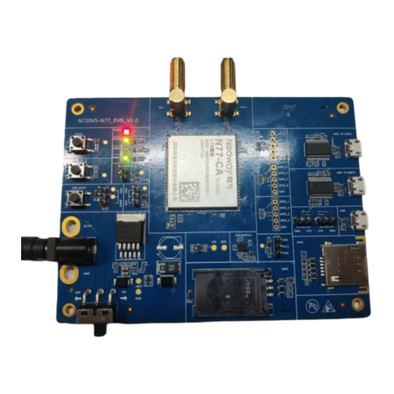
- Page 9 N77 Hardware User Guide About This Document Related Documents Neoway_N77-CA_Datasheet Neoway_N77-CA_Product_Specifications Neoway_N77-CA_AT_Commands_Mannual Neoway_N77-CA_EVK_User_Guide Copyright © Neoway Technology Co., Ltd.
-
Page 10: About N77
WCDMA: B1, B5, B8 GSM/GPRS/EDGE: 900/1800 MHz N77 adopts 100-pin LGA package and its dimensions are 30mm x 28mm x 2.6mm. With industrial- grade performance, it is well applicable to the wireless meter reading terminal walkie-talkie, handheld POS, and other IoT terminals. -
Page 11: Basic Features
In standby mode, the module is in normal working state, but there is no on-going data service. Copyright © Neoway Technology Co., Ltd. - Page 12 Commands defined in 3GPP TS 27.007 3GPP TS 27.005, and Neoway AT commands extended AT commands PDU, TXT Data PPP, RNDIS Protocol TCP/TCPS, UDP, HTTP/HTTPS, FTP, MQTT Certification CCC, SRRC, CTA, RoHS (Related certification processes are under way.) approval Copyright © Neoway Technology Co., Ltd.
-
Page 13: Module Pins
N77 Hardware User Guide Chapter 2 Module Pins 2 Module Pins The N77 module has a total of 100 pins, adopts LGA package, and supports the following functional interfaces: 2.1 Pin Layout Figure 2-1 shows the N77 pin layout. Figure 2-1 N77 pin definition... -
Page 14: Pin Description
= 1.2V IH min = 2.0V IH min USB2.0 data interface Table 2-2 Pin description Power Signal Function Level Feature Remarks Domain Power interface VBAT 27, 28, Main power V = 4.3V power All rights reserved by Neoway Technology Co., Ltd. - Page 15 Module power- PWRKEY VBAT high level. on control Leave this pin floating if it is not used. Status indication Sleep mode It controls the SLEEP 1.8V control sleep mode of All rights reserved by Neoway Technology Co., Ltd.
- Page 16 Data receiving 1.8V data transmission and debugging. UART2_TX Data Leave this pin 1.8V transmitting floating if it is not used. USIM interface 1.8V USIM: =1.9V USIM power =1.7V USIM_VCC output 3.0V USIM: =3.1V All rights reserved by Neoway Technology Co., Ltd.
- Page 17 Leave this pin floating if it is not used. 12-bit. Detectable Universal =1.3V; voltage range: ADC2 analog-to- – =0.1V 1.3V. digital signal Leave this pin floating if it is not All rights reserved by Neoway Technology Co., Ltd.
- Page 18 Leave this pin SPI_MOSI and output of 1.8V floating if it is not master used. device Chip select Leave this pin SPI_CS_N signal 1.8V floating if it is not slave device used. All rights reserved by Neoway Technology Co., Ltd.
- Page 19 The GPIO is equipped with the interrupt function. If you need to use the interrupt function, contact our FAE; otherwise, the software interrupt priority may be abnormal and unpredictable risks may arise when the module is running. All rights reserved by Neoway Technology Co., Ltd.
- Page 20 *USB_BOOT cannot be pulled up to 1.8V output by the module. If you need to use the boot upgrade method, the pin should be pulled up to the external stable 1.8V in the design All rights reserved by Neoway Technology Co., Ltd.
- Page 21 N77 Hardware User Guide Chapter 2 Module Pins Leave this pin 3,4, 5, 6, 7, 8, 21, 43, 53, 84, RESERVED floating if it is not 85, 86, 87, 90, 92 used. All rights reserved by Neoway Technology Co., Ltd.
-
Page 22: Application Interfaces
The power supply design consists of two parts: circuit design and PCB layout. Power Supply Design N77 supports the 3.4V-4.3V power input (typical value: 3.8V, using the battery for power supply). Recommended designs are as follows: All rights reserved by Neoway Technology Co., Ltd. -
Page 23: Figure 3-1 Recommended Design 1
D102 10 μF 0.1 μF 33 pF 100pF C106 C107 C113 R101 10 μF 0.1 μF C114 1 μF 0.1 μF 100 k R104 10 k R102 PWR_EN Q102 R103 10 k All rights reserved by Neoway Technology Co., Ltd. -
Page 24: Figure 3-3 Recommended Design 3
Its withstand voltage should be larger than 1.5 times the voltage of the power supply. Place a bypass capacitor of low-ESR close to the module to filter out high-frequency jamming ⚫ from the power supply. All rights reserved by Neoway Technology Co., Ltd. -
Page 25: Vdd_1P8
3.1.2 VDD_ N77 provides one VDD_1P8 output. It can provide the 1.8V voltage and the maximum output current is 50mA. VDD_1P8 does not need to be controlled and it is automatically open when the module wakes up, is started, or is in normal working state. -
Page 26: Pwrkey_N
Figure 3-5 Reference design of startup controlled by MCU PWRKEY_N USER_ON R302 Q301 4.7kΩ N77 module R303 47kΩ Figure 3-6 Reference design of automatic start once powered up PWRKEY_N kΩ N77 module All rights reserved by Neoway Technology Co., Ltd. -
Page 27: Pwrkey
Do not perform other operations on the module until it is initialized completely. If the module is powered on but the power-on process has not been completed, the states of each pin are uncertain. Figure X- X shows the startup timing. All rights reserved by Neoway Technology Co., Ltd. -
Page 28: Figure 3-8 Startup Process
Hard shutdown is implemented through the RESET_N pin. When the module is working, inputting low level pulse for over 10s to RESET_N can trigger shutdown of the module. The following figure shows the hard shutdown process. All rights reserved by Neoway Technology Co., Ltd. -
Page 29: Reset_N
If the 1.8V/2.8V/3.0V IO system is used, it is recommended that a triode be used for isolation. For details about the design, see the following two figures. To use the high level for reset, refer to Figure 3-5 MCU power-on control circuit. All rights reserved by Neoway Technology Co., Ltd. -
Page 30: Figure 3-10 Reset Controlled By Button
N77 module VDD_1P8 In the 1.8V/2.8V/3.0V system shown in Figure 3-11, R2 is equal to 5.1Ω, and R1 is equal to 4.7K. The following figure shows the reset process of the N77 module. All rights reserved by Neoway Technology Co., Ltd. -
Page 31: Peripheral Interfaces
USB data positive signal the differential impedance must be 90Ω. N77 can implement program download, data communication, and debugging through the USB interface. The USB of the module is a USB device, which can be selected by users based on actual requirements. -
Page 32: Uart
3.3.2 UART Signal Function Description Remarks When the device is started, DEBUG_UART1_TX Data transmitting some logs are output. Leave this pin unconnected when it All rights reserved by Neoway Technology Co., Ltd. -
Page 33: Figure 3-14 Uart Connection
Schematic design guidelines: ⚫ Pay attention to the mapping relationship of signals. ⚫ By default, the flow control function is disabled. If this function must be enabled, contact the Neoway technical support engineers. All rights reserved by Neoway Technology Co., Ltd. -
Page 34: Figure 3-15 Recommended Level Shifting Circuit 1
If the level signal quality of the MCU is good and the rate requirement is not high (the maximum baud rate is 115200), another serial port level shifter is recommended, as shown in the recommended circuit All rights reserved by Neoway Technology Co., Ltd. -
Page 35: Usim
USIM1 clock output USIM1_RESET USIM1 reset USIM1_DET USIM1 detection N77 provides a set of USIM card interfaces, which can automatically adapt to the 1.8V/3.0V USIM card. Figure 3-17 shows the reference design. All rights reserved by Neoway Technology Co., Ltd. -
Page 36: Figure 3-17 Reference Design Of The Usim Card Interface
USIM card is detected, and the high level indicates that the USIM card is not detected. (By default, the low level is used to detect the SIM card socket.) PCB design guidelines: All rights reserved by Neoway Technology Co., Ltd. -
Page 37: Spi
The following figures provide the reference design, sequence diagram, and parameters. Figure 3-18 SPI connection MISO SPI_MISO SPI_MOSI MOSI SPI_CS_N SPI_CLK N77 module SPI device (host) (device) Figure 3-19 SPI timing 3.3.5 IIC Signal Function Description Remarks IIC_SDA I2C data All rights reserved by Neoway Technology Co., Ltd. -
Page 38: Adc
I2C data up from 4.7V to 1.8V. The N77 module provides two I2C interfaces, which conform to the IIC Specification 5.0 (released on October 2012) and only support the master device mode. The IIC interface can a rate up to 3.3Mbps, and the interface reference high level is 1.8V. -
Page 39: Sleep
Pull down the SLEEP pin of the module The module Is the module completes the current currently in idle state? service processing The module enters the sleep mode All rights reserved by Neoway Technology Co., Ltd. -
Page 40: Figure 3-23 Service Execution Process When The Module Is In Sleep Mode
Performing an MO service when the module is Performing an MT service when the module is in sleep mode in sleep mode The basic process for the module to exit the sleep mode is as follows: All rights reserved by Neoway Technology Co., Ltd. -
Page 41: Net_Light
The NET_LIGHT pin outputs a high level of 1.8V. It is prohibited to directly use it to drive the LED indicator. It is recommended that you use the transistor to drive the LED indicator. The specific reference design is shown in the figure below. All rights reserved by Neoway Technology Co., Ltd. -
Page 42: Ring
30 ms 30 ms Incoming SMS ⚫ When there is an incoming SMS, the RING pin generates a low pulse prompt with a pulse width of 35ms, as shown in the following figure. All rights reserved by Neoway Technology Co., Ltd. -
Page 43: Usb_Boot
10 kΩ VREG_1V8 USB_BOOT S301 ESD301 3.3.11 GPIO N77 provides 15 GPIO interfaces, all of which have the interrupt function. The AT commands can be used to control the GPIO status. Signal Function Description GPIO_01 GPIO with the interrupt function... -
Page 44: Rf Interface
4G diversity antenna pin 3.4.1 Antenna Interface The antenna interface of the N77 requires the 50Ω impedance feature. The impedance of the cable from the module interface to the antenna needs to be kept at 50Ω impedance to ensure RF performance. -
Page 45: Figure 3-29 L-Type Network
You can use a TVS tube with ultra-low junction capacitance. It is recommended that you use a TVS tube with a junction capacitance less than 0.5pF. In addition, you must ensure that All rights reserved by Neoway Technology Co., Ltd. -
Page 46: Antenna Assembling
Inverted F antenna (PIFA). Keep external RF wires far away from all disturbing sources, especially digital signals and DC/DC power if using RF wires. The following methods are commonly used to assemble antenna: All rights reserved by Neoway Technology Co., Ltd. -
Page 47: Figure 3-33 Specifications Of Mm9329-2700Ra1
PCB after the design phase is completed. They are used only for 2.4G Wi-Fi or Bluetooth because they cannot cover wide frequencies. The following figure shows the layout of the 2.4G ceramic chip antenna. SLDA52-2R540G-S1TF is used as an example. All rights reserved by Neoway Technology Co., Ltd. -
Page 48: Figure 3-35 Antenna Layout
Figure 3-36 shows the layout for the area between the antenna and ground that is marked as "5" in Figure 3-35. Figure 3-36 Layout around the antenna For more details, refer to the antenna manuals and other documents. All rights reserved by Neoway Technology Co., Ltd. -
Page 49: Electric Feature And Reliability
Chapter 4 Electric Feature and Reliability 4 Electric Feature and Reliability This chapter describes the electrical characteristics and reliability of the N77 module, including the input and output voltage and current of the power supply, current consumption of the module in different states, operating and storage temperature range, and ESD protection characteristics. -
Page 50: Temperature Features
Table 4-3 N77 ESD protection features Testing Point Contact Discharge Air Discharge VBAT ± 8KV ± 15KV ± 8KV ± 15KV ± 8KV ± 15KV Cover ± 8KV ± 15KV Others ± 2KV ± 4KV All rights reserved by Neoway Technology Co., Ltd. -
Page 51: Rf Features
N77 Hardware User Guide Chapter 5 RF Features 5 RF Features The N77 module supports the GSM, WCDMA, FDD-LTE, TDD-LTE (Cat4) networks. This chapter describes the RF features of N77. 5.1 Operating Bands Table 5-1 N77 operating bands Operating Bands... -
Page 52: Tx Power And Rx Sensitivity
N77 Hardware User Guide Chapter 5 RF Features 5.2 TX Power and RX Sensitivity Table 5-2 N77 RF TX power and RX sensitivity Band Max Power Min. Power EGSM900 33dBm+2/-2dB 5dBm+2/-2dB DCS1800 30dBm+2/-2dB 0dBm+2/-2dB WCDMA B1 24dBm +1/-3dBm <-49 dBm... - Page 53 The preceding indexes are test data in a laboratory environment. The test results of LTE(Cat 4) in a bandwidth of 10MHz will have a certain deviation due to the influence of the network environment. All rights reserved by Neoway Technology Co., Ltd.
-
Page 54: Mechanical Features
This chapter describes mechanical features of the N77 module. 6.1 Dimensions Figure 6-1 N77 dimensions (Unit: mm) 6.2 Label The label information is laser carved on the cover. The following figure shows the label of N77. All rights reserved by Neoway Technology Co., Ltd. -
Page 55: Packing
⚫ 6.3 Packing The N77 module adopts the SMT method for oven soldering. To prevent the products from being damp before they are delivered to customers, the tray is used for moisture-proof packaging. The aluminum foil bag, desiccant, humidity indicator card, tray, vacuum and other processing methods are used to ensure the dryness of the product and extend its service life. -
Page 56: Moisture
N77 Hardware User Guide Chapter 6 Mechanical Features 6.4 Moisture N77 is a level 3 moisture-sensitive electronic elements, in compliance with IPC/JEDEC J-STD-020 standard. If the module is exposed to air for more than 48 hours at conditions not worse than 30°C/60% RH, bake it at a temperature higher than 90 °C for more than 12 hours before SMT. -
Page 57: Mounting N77 Onto Application Pcb
N77 Hardware User Guide Chapter 7 Mounting N77 onto Application PCB 7 Mounting N77 onto Application PCB This chapter describes the package of N77, the recommended footprint of the application PCB, and SMT specifications.. 7.1 Bottom Dimensions Figure 7-1 N77 Bottom view of PCB package (Unit: mm) -
Page 58: Application Foot Print
N77 Hardware User Guide Chapter 7 Mounting N77 onto Application PCB 7.2 Application Foot Print Figure 7-2 Recommended footprint of N77 application PCB (Unit: mm) 7.3 Stencil The recommended stencil thickness is at least 0.12 mm to 0.15 mm. All rights reserved by Neoway Technology Co., Ltd. -
Page 59: Solder Paste
N77 Hardware User Guide Chapter 7 Mounting N77 onto Application PCB 7.4 Solder Paste The quality of the solder joint depends on the solder paste volume and the PCB flatness. Do not use the kind of solder paste different from our module technique. - Page 60 Neoway will not provide warranty for heat-responsive element abnormalities caused by improper temperature control. For information about cautions in N77 storage and mounting, refer to Neoway Module Reflow Manufacturing Recommendations. When manually desoldering the module, use heat guns with great opening, adjust the temperature to 245 °C (depending on the type of the solder paste), and heat the module till the solder paste is melt.
-
Page 61: Safety Recommendations
If the product is used in medical institutions or on airplanes, electromagnetic waves emitted by this product may interfere with surrounding equipment. Please follow the requirements below in application design: Do not disassemble the module without permission from Neoway. Otherwise, we are entitled to ⚫ refuse to provide further warranty. -
Page 62: Bom
N77 Hardware User Guide A BOM TBD. All rights reserved by Neoway Technology Co., Ltd. -
Page 63: Abbreviation
GPIO General Purpose Input Output 3GPP 3rd Generation Partnership Project GPRS General Packet Radio Service Global Positioning System Global System for Mobile Communications Inter-Integrated Circuit Input/Output Light Emitting Diode Long Term Evolution All rights reserved by Neoway Technology Co., Ltd. - Page 64 Real Time Clock Subscriber Identification Module Serial Peripheral Interface Time Division Duplex UART Universal asynchronous receiver-transmitter Universal Serial Bus USIM Universal Subscriber Identity Module VBAT Battery Voltage VSWR Voltage Standing Wave Ratio All rights reserved by Neoway Technology Co., Ltd.
Need help?
Do you have a question about the N77 and is the answer not in the manual?
Questions and answers