Advertisement
Quick Links
User Guide
I N T R O D U C T I O N
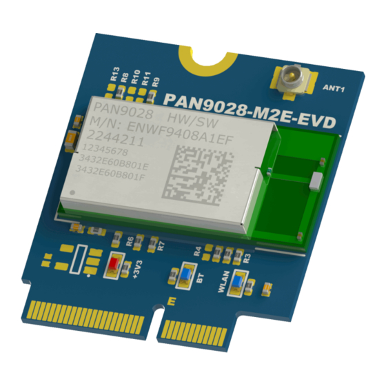
The PAN9028 M.2 device (ENWF9408AMEF) is an evaluation device (EVD) ideally
suited for use of the module in conjunction with host processor evaluation kits that
have a M.2 Key E socket.
It features a PAN9028 with an integrated Power Management IC
(ENWF9408A1EF).
F E A T U R E S
M.2 Key E form factor
External antenna U.FL connector
Coexistence interface
Wi-Fi and Bluetooth status indicator LEDs
Advertisement

Subscribe to Our Youtube Channel
Related Manuals for Element14 PAN9028 M.2


Summary of Contents for Element14 PAN9028 M.2
- Page 1 User Guide I N T R O D U C T I O N The PAN9028 M.2 device (ENWF9408AMEF) is an evaluation device (EVD) ideally suited for use of the module in conjunction with host processor evaluation kits that have a M.2 Key E socket.
- Page 2 PCM interface B L O C K D I A G R A M PAN9028 M.2 Device Status LEDs Highspeed-UART for Bluetooth SDIO 3.0 for Wi-Fi M.2 Key E Module Connector Interface Coexistence Interface U.FL Connector External Antenna B O A R D O V E R V I E W...
- Page 3 The Bluetooth status indicator LED for indicating the Bluetooth status is currently non-operational. M.2 Key E connector You can insert the PAN9028 M.2 device into a M.2 Key E socket to connect the modules interfaces to a host processor. Also see M.2 Connector Pin Map Power LED You can observe the Power LED to verify that the board is correctly powered.
-
Page 4: Mounting The Device
I N I T I A L P R E P A R A T I O N S Mounting the Device To mount the PAN9028 M.2 device in a M.2 Key E socket on a host board execute the following instructions. - Page 5 2. Insert the PAN9028 M.2 device into the socket slightly angled. 3. Apply some light downward pressure until the PAN9028 M.2 device is parallel to the host board and makes contact to the threaded insert. 4. Insert a M2.5 x 4 machine screw into the mounting screw indentation the threaded insert.
- Page 6 The PAN9028 M.2 device is secured in place. M . 2 C O N N E C T O R P I N M A P Description M.2 Key Function Module Module Pin E Pin Footprint SDIO SDIO CLK SD_CLK...
- Page 7 Description M.2 Key Function Module Module Pin E Pin Footprint I2S SCK / GPIO6 PCM_CLK / IO6 Interface I2S WS / GPIO7 PCM_SYNC / I2S SD IN / GPIO5 PCM_DOUT / I2S SD OUT / PCM_DIN / IO4 GPIO4 Coexistence Coexistence RXD / COEX_OUT / Interface...
- Page 8 Description M.2 Key Function Module Module Pin E Pin Footprint 3, 5, 7, not connected connected 21, 23, 35, 37, 38, 40, 41, 42, 43, 44, 47, 49, 52, 53, 54, 55, 58, 59, 60, 61, 62, 64, 65, 66, 67, 68, 70, 71,...
- Page 9 U.FL connector ANT1 SDIO Reference Voltage In case your host processor board only supports a SDIO signal voltage of 3.3 V you can reconfigure the PAN9028 M.2 device to use the 3.3 V generated by the PMIC as V IOSD The PAN9028 supports 1-bit or 4-bit SDIO transfer modes with full clock range up to 208 MHz.
- Page 10 IO Reference Voltage Setting V to 3.3 V also configures the IO reference voltage to IOSD be 3.3 V as well. To set V to 3.3 V execute the following instructions. IOSD 1. Unsolder the resistors R8 and R9. 2. Place a 0 Ohm resistor (0402) for R13 and or bridge it with a solder blob. 3.
- Page 11 IO Reference Voltage In case your host processor board supports only IO voltage levels of 3.3 V you can reconfigure the PAN9028 M.2 device to use 3.3 V as voltage level for its UART and IOs. The voltage used by the IOs and the UART interface is determined by the voltage applied to V .
- Page 12 On the PAN9028 M.2 device by default V is connected to V of the PMIC, OUT1V8 hence it is set to 1.8 V. Warning In case you have set V to 3.3 V as described in IOSD SDIO Reference Voltage the IO reference voltage is also configured to be 3.3 V.
-
Page 13: Antenna Configuration
This connects V to 3.3 V. Antenna Configuration You can evaluate PAN9028 M.2 device in conjunction with an external antenna by activating the external antenna U.FL connector ANT1 with some hardware modifications. By default the chip antenna is active. External Antenna To activate the external antenna U.FL connector ANT1... - Page 14 Chip Antenna In case you modified the PAN9028 M.2 device to use the external antenna U.FL connector ANT1 execute the following instructions to switch back to the chip antenna. 1. Unsolder R4. 2. Place a 0 Ohm resistor (0402) for R3 or bridge it with a solder blob.
Need help?
Do you have a question about the PAN9028 M.2 and is the answer not in the manual?
Questions and answers