
Related Manuals for LG SJ5


Summary of Contents for LG SJ5
- Page 1 Internal Use Only Wireless Sound Bar SERVICE MANUAL MODEL: SJ5 (SJ5, SPJ5-W) CAUTION BEFORE SERVICING THE UNIT, READ THE “SAFETY PRECAUTIONS” IN THIS MANUAL. P/NO : AFN77558564 JANUARY, 2017...
- Page 2 CONTENTS SECTION 1 ..GENERAL SECTION 2 ..CABINET & MAIN CHASSIS SECTION 3 ..ELECTRICAL SECTION 4 ..WIRELESS SUBWOOFER PART...
-
Page 3: Table Of Contents
SECTION 1 GENERAL CONTENTS ESD PRECAUTIONS ............................1-3 NAME OF EACH COMPONENT ........................1-4 WIRELESS SUBWOOFER CONNECTION ....................... 1-5 HIDDEN KEY MODE ............................1-6 SOFTWARE UPDATE GUIDE ........................... 1-7 SPECIFICATIONS ............................1-13... -
Page 4: Esd Precautions
ESD PRECAUTIONS Electrostatically Sensitive Devices (ESD) Some semiconductor (solid state) devices can be damaged easily by static electricity. Such components commonly are called Electrostatically Sensitive Devices (ESD). Examples of typical ESD devices are integrated circuits and some field-effect transistors and semiconductor chip components. The following techniques should be used to help reduce the incidence of component damage caused by static electricity. -
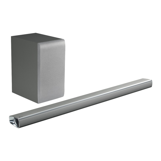
Page 5: Name Of Each Component
NAME OF EACH COMPONENT • Front Panel C The buttons are located on the rear. • Rear Panel A o/p : B DC IN : C OPTICAL IN : D PORTABLE IN : 1 (Standby) E USB F HDMI OUT (TV ARC) / IN :... -
Page 6: Wireless Subwoofer Connection
WIRELESS SUBWOOFER CONNECTION LED indicator of wireless subwoofer Note : • It takes a few seconds (and may take longer) for the main unit and the subwoofer to communicate with LED Color Status each other and make sounds. Green • The closer the main unit and the subwoofer, the Attempting to make connection. -
Page 7: Hidden Key Mode
HIDDEN KEY MODE HIDDEN MODE KEYS EEPROM OPTION EDIT Main unit ' (Volume)' + Remote control ' (Night Mode)' for more than 3 seconds. Main unit ' (Volume)' + Remote control 'SOUND EFFECT' for more than 3 seconds. EEPROM CLEAR (Initialize) Display window : "E-CLR"... -
Page 8: Software Update Guide
1-1. Preparation - Remote control. - Do format USB Memory to FAT32 File system. - USB : Update fi le exist only in the USB Memory stick. Ex ) SJ5 : MAIN E:\DSP_MAIN_SJ5.ROM (if USB driver is E:\) MICOM ... - Page 9 2. Using APP (FOTA : Firmware update Over The Air) 2-1. Run BT App (Music Flow Bluetooth) 2-2. Connect Bluetooth Menu button Connection button < Not Connected > < Connected >...
- Page 10 Using APP (FOTA : Firmware update Over The Air) 2-3. Setting Menu 2-4-1. FOTA Start Button (Phone should be available internet, Wi-Fi, LTE, Setting button FOTA Start button < Connected > < Internet not Connected > • Some Country(ex China) can not access to CDN Server.
- Page 11 Using APP (FOTA : Firmware update Over The Air) 2-4-2. FOTA Start Button 2-5. FOTA Caution button FOTA Start button < Internet Connected > 1-10...
- Page 12 Using APP (FOTA : Firmware update Over The Air) 2-6. FOTA - CDN Download 2-7. FOTA - OPP Download Cancel Cancel button button Cancel Button is available Cancel Button is not available When CDN downloading. When OPP downloading. 1-11...
- Page 13 Using APP (FOTA : Firmware update Over The Air) 2-8. FOTA - Write Flash 2-9. FOTA - Finish Power cable reconnect. Cancel button Cancel Button is not available When Flash writing. 1-12...
-
Page 14: Specifications
SPECIFICATIONS • GENERAL Power consumption Refer to the main label. Networked standby : 0.5 W (If all network ports are activated.) AC adapter Model : DA-38A25 Manufacturer : Asian Power Devices Inc. Input : 100 - 240 V ~ 50 - 60 Hz 1.2 A Output : 25 V 1.52 A Dimensions (W x H x D) - Page 15 1-14...
- Page 16 SECTION 2 CABINET & MAIN CHASSIS CONTENTS DISASSEMBLY INSTRUCTIONS ........................2-2 1. HOW TO DISASSEMBLE THE MAIN UNIT ..................... 2-2 2. HOW TO DISASSEMBLE THE SUBWOOFER ..................2-8 EXPLODED VIEWS ............................2-11 1. MAIN UNIT SECTION ..........................2-11 2. WIRELESS SUBWOOFER SECTION ....................2-13 3.
-
Page 17: Disassembly Instructions
DISASSEMBLY INSTRUCTIONS 1. HOW TO DISASSEMBLE THE MAIN UNIT ※ Before begin, position the Main Unit upside down. 1-1. Case Bottom Assembly 1) Remove the 21 screws. 2) Remove the Case Bottom Assembly. Case Bottom Assembly Figure 1-1... -
Page 18: How To Disassemble The Main Unit
HOW TO DISASSEMBLE THE MAIN UNIT 1-2. Main Frame Assembly 1) Disconnect the 3 harness cables from the Main PCB Assembly. Figure 1-2 (1) 2) Remove the screw. 3) Remove the Main Frame Assembly (Main Chassis + PCBA). Main Frame Assembly Figure 1-2 (2) - Page 19 HOW TO DISASSEMBLE THE MAIN UNIT 1-2-1. Front PCB Assembly 1) Remove the 2 screws. 2) Remove the Front PCB Assembly. Front PCB Assembly Figure 1-2-1 1-2-2. Main PCB Assembly 1) Detach the cables from the Main chassis. 2) Disconnect the FFC cables from the Main PCB Assembly. 3) Remove the 3 screws (Main + HDMI Jack).
- Page 20 HOW TO DISASSEMBLE THE MAIN UNIT 1-2-3. BT and WIRELESS Module 1) Disconnect the FFC cable from the BT module. 2) Remove the BT module. 3) Disconnect the FFC cable from the WIRELESS module. 4) Disconnect the 2 Hooks. 5) Remove the WIRELESS module. BT Module WIRELESS Module Figure 1-2-3...
- Page 21 HOW TO DISASSEMBLE THE MAIN UNIT 1-3. SPEAKER CHAMBER L/R Assembly 1) Remove the Speaker Chamber L/R Assembly. Speaker Chamber Right Assembly Speaker Chamber Left Assembly Figure 1-3 1-4. KEY PCB Assembly 1) Remove the KEY PCB Assembly. KEY PCB Assembly Figure 1-4...
- Page 22 HOW TO DISASSEMBLE THE MAIN UNIT 1-5. How to organize cables When assembling, place the cables (Speaker network cables and Key cable) as shown in the fi gure below. Figure 1-5 (1). < Harness cable from KEY PCB to MAIN PCB > Figure 1-5 (2).
- Page 23 2. HOW TO DISASSEMBLE THE SUBWOOFER 2-1. Rear Panel Assembly 1) Remove the 13 screws. Figure 2-1 (1) 2) Pull out the Rear Panel Assembly and disconnect the SPK cable. Rear Panel Assembly SPK cable Figure 2-1 (2)
-
Page 24: How To Disassemble The Subwoofer
HOW TO DISASSEMBLE THE SUBWOOFER 2-2. WIRELESS Module 1) Disconnect the FFC cable. 2) Remove the EVA sheet (0.15T) covered the WIRELESS module. 3) Remove the WIRELESS module. 4) Remove the EVA gasket (1.0T) covered the WIRELESS module. AMP+SMPS PCB Assembly Figure 2-2 (1) Caution when assembling the WIRELESS Module 1) Attach the EVA gaskets (1.0T) to both sides of the WIRELESS module. - Page 25 HOW TO DISASSEMBLE THE SUBWOOFER 2-3. AMP+SMPS PCB Assembly 1) Disconnect the Power inlet socket cable. AMP+SMPS PCB Assembly Figure 2-3 (1) 2) Remove the 5 screws. 3) Remove the AMP+SMPS PCB Assembly. AMP+SMPS PCB Assembly Figure 2-3 (2) 2-10...
-
Page 26: Exploded Views
EXPLODED VIEWS 1. MAIN UNIT SECTION NOTES) THE EXCLAMATION POINT WITHIN AN EQUILATERAL TRIANGLE IS INTENDED TO ALERT THE SERVICE PERSONNEL TO THE PRESENCE OF IMPORTANT SAFETY INFORMATION IN SERVICE LITERATURE. A80R MAIN FRONT 271R CABLE2 LCD01 CABLE3 CABLE1 A80L WIRELESS 271L 2-11... -
Page 27: Wireless Subwoofer Section
2. WIRELESS SUBWOOFER SECTION A900 A900W A45W A54W 2-13 2-14... -
Page 28: Packing Accessory Section
3. PACKING ACCESSORY SECTION 801 Owner’s manual 806 Optical cable 900 Remote control 808 Batteries (2) 833 AC adapter 300 Power cord 836 Screws (2) 835 Wall bracket 804 Bag 803 Packing, Main 802 Box 2-15... - Page 29 2-16...
- Page 30 SECTION 3 ELECTRICAL CONTENTS WIRING DIAGRAM ............................3-2 BLOCK DIAGRAMS ............................3-3 1. SYSTEM BLOCK DIAGRAM ........................3-3 2. POWER BLOCK DIAGRAM ........................3-4 ONE POINT REPAIR GUIDE ..........................3-5 1. NO BOOTING WHEN YOU TURN THE UNIT ON, NO MESSAGE OR “HELLO” ON FRONT PANEL ..........................
-
Page 31: Wiring Diagram
WIRING DIAGRAM CN704 CN703... -
Page 32: Block Diagrams
BLOCK DIAGRAMS 1. SYSTEM BLOCK DIAGRAM... -
Page 33: Power Block Diagram
2. POWER BLOCK DIAGRAM... -
Page 34: One Point Repair Guide
ONE POINT REPAIR GUIDE 1. NO BOOTING WHEN YOU TURN THE UNIT ON, NO MESSAGE OR “HELLO” ON FRONT PANEL When you turn on your set, no message on the front panel, and stand-by LED doesn’t work. 1-1. IC302 System 12 VA (No 12 VA) 1-1-1. - Page 35 ONE POINT REPAIR GUIDE NO BOOTING WHEN YOU TURN THE UNIT ON, NO MESSAGE OR “HELLO” ON FRONT PANEL When you turn on your set, it will blank / no message on front panel, and stand-by LED doesn’t work. 1-2. IC301 System 3.3 V (No 3.3 VA) 1-2-1.
- Page 36 ONE POINT REPAIR GUIDE NO BOOTING WHEN YOU TURN THE UNIT ON, NO MESSAGE OR “HELLO” ON FRONT PANEL When you turn on your set, it will blank / no message on front panel, and stand-by LED doesn’t work. 1-3. LCD System power 5 V, 3.3 VA (No 5 V, 3.3 VA) 1-3-1.
- Page 37 ONE POINT REPAIR GUIDE 2. NO SOUND 2-1. BLUETOOTH 2-1-1. Solution Replace MAIN board. 2-1-2. How to troubleshoot (Countermeasure) 1) Please check status of Bluetooth cable connection. (at CN102 and BT module) 2) Please check 3.3 VA (at pin1 of CN102). If 3.3 V is OK, please check BT_RST, BT_SPDIF, BT_RX, BT_TX (pin2, 4, 11, 12).
-
Page 38: Sound
ONE POINT REPAIR GUIDE NO SOUND 2-2. OPTICAL 2-2-1. Solution Replace MAIN board. 2-2-2. How to troubleshoot (Countermeasure) 1) Please check 3.3 VA at R209. 2) If 3.3 VA is ok, please check OPT_IN signal (C208) when OPTICAL mode. 3) If signal is abnormal, replace MAIN board. 2-2-3. - Page 39 ONE POINT REPAIR GUIDE NO SOUND 2-3. HDMI 2-3-1. Solution Replace MAIN board. 2-3-2. How to troubleshoot (Countermeasure) 1) Please check soldering status of HDMI jack and check HDMI_5.1VA at IC308 pin1. 2) If soldering status and 5.1 VA are abnormal, replace MAIN board. 2-3-3.
- Page 40 ONE POINT REPAIR GUIDE NO SOUND 2-4. PORTABLE 2-4-1. Solution Replace MAIN board. 2-4-2. How to troubleshoot (Countermeasure) 1) Please check the soldering status of portable jack and check IC201 pin3 (VCC_5V), pin4 (D_3.3V). 2) If portable jack and voltage has abnormal status, replace MAIN board. 2-4-3.
- Page 41 ONE POINT REPAIR GUIDE NO SOUND 2-5. USB 2-5-1. Solution Replace MAIN board. 2-5-2. How to troubleshoot (Countermeasure) 1) Please check USB Jack and FB201 soldering status. And check 5 V at JK201 pin1. 2) If soldering status and voltage has abnormal status, replace MAIN board. 2-5-3.
- Page 42 ONE POINT REPAIR GUIDE 3. PROTECTION ERROR No display or No Sound. 3-1. D(DC) PROTECTION 3-1-1. Solution Replace MAIN board. 3-1-2. How to troubleshoot (Countermeasure) 1) Check DC Voltage of speaker out FL+/-, TWL+/- (CN703 pin1, 2, 3, 4) and FR+/-, TWR+/- (CN704 pin1, 2, 4, 5). 2) Check resistor crack, cold solder of PWM IC out (AR601, AR602) 3) If PWM IC out is ok and speaker out (FL+/-, FR+/-, TWL+/-, TWR+/-) has DC voltage, replace MAIN board.
-
Page 43: Protection Error
ONE POINT REPAIR GUIDE PROTECTION ERROR No display or No Sound. 3-2. S(SHUT DOWN) PROTECTION 3-2-1. Solution Replace MAIN board. 3-2-2. How to troubleshoot (Countermeasure) 1) Check PVDD voltage (25 V) of IC700, IC701 pin38, 37, 36. - If PVDD voltage has 8.5 V under, refer to STEP 1-1. 2) Check GVDD, VDD voltage (12 V) of IC700, IC701 pin1, 2. - Page 44 ONE POINT REPAIR GUIDE PROTECTION ERROR No display or No Sound. 3-3. B(BURNT) PROTECTION 3-3-1. Solution Replace MAIN board. 3-3-2. How to troubleshoot (Countermeasure) 1) Check voltage 12 V of IC700, IC701 at pin1 ~ 2, if 12 V has problem refer to STEP 1-1. 2) If 12 V is OK, replace MAIN board.
-
Page 45: Waveforms Of Major Check Point
WAVEFORMS OF MAJOR CHECK POINT 1. CRYSTAL FIG 1-1. X501 (27 MHz) FIG 1-2. X600 (24.576 MHz) 2. FLASH MEMORY FIG 2. VCC, CS#, CLK, DO 3-16... -
Page 46: Tact Key
3. TACT KEY 1 ~ 1.13 V 0.72 ~ 0.82 V FIG 3-2. Press FUNC Key FIG 3-1. Press Power Key 0.424 ~ 0.485 V FIG 3-3. Press VOL - Key FIG 3-4. Press VOL + Key 3-17... -
Page 47: Usb
4. USB FIG 4-1. 5 V Voltage FIG 4-2. USB D+ FIG 4-3. USB D- 3-18... -
Page 48: Remote Control
5. REMOTE CONTROL FIG 5-1. Input Voltage 12 13 FIG 5-2. Low Timing Item Measured Spec. IR Receiver Spec: Input Level 3.3 V 2.7 ~ 5.5 V “ Low” Timing 4.4 ms 3.6 ms ~ 5.04 ms “ High” Timing 4.48 ms 4.08 ms ~ 5.04 ms FIG 5-3. -
Page 49: Optical
6. OPTICAL FIG 6-1. OPT_IN FIG 6-2. OPT_DET 3-20... -
Page 50: Portable
7. PORTABLE FIG 7-1. ADC IC 5 V FIG 7-2. ADC IC 3.3 V 1 1 .27 Vrms FIG 7-3. Analog Input Voltage 3-21... - Page 51 3-22...
-
Page 52: Circuit Voltage Chart
CIRCUIT VOLTAGE CHART 1. IC VOLTAGE 2. CAPACITOR VOLTAGE Measured Temperature Designator Description SPEC Real Value (#1, #2)/ V Temperature Spec. Designator Description Pin No Pin Name Voltage Spec Voltage Spec. C390, C734, AVCC 1.8 V ~ 3.6 V 3.34 V Capacitor,AL,Chip 330 uF/ 35 V 25.76... -
Page 53: Printed Circuit Board Diagrams
PRINTED CIRCUIT BOARD DIAGRAMS 1. MAIN P. C. BOARD DIAGRAM (TOP VIEW) (BOTTOM VIEW) 3-25 3-26... -
Page 54: Front P. C. Board Diagram
2. FRONT P. C. BOARD DIAGRAM (TOP VIEW) (BOTTOM VIEW) 3. KEY P. C. BOARD DIAGRAM (TOP VIEW) (BOTTOM VIEW) 3-27 3-28... - Page 55 3-29 3-30...
- Page 56 SECTION 4 WIRELESS SUBWOOFER PART CONTENTS WIRING DIAGRAM ............................4-2 BLOCK DIAGRAM ............................4-3 ONE POINT REPAIR GUIDE ..........................4-4 1. POWER ON ERROR ..........................4-4 2. WIRELESS CONNECTION ........................4-6 WAVEFORMS OF MAJOR CHECK POINT ...................... 4-7 1. CRYSTAL ..............................4-7 2.
-
Page 57: Wiring Diagram
WIRING DIAGRAM 2P, 3.96mm ST, Non Lock SMD Wireless 26P, 0.5mm ST, Non Lock SMD 2P, 3.96mm ST, Non Lock , SMD Power... -
Page 58: Block Diagram
BLOCK DIAGRAM Wireless LED (RED, GREEN) Wireless AMP_PDN AMP_SD PAIRING Reset KEY SW+/SW- PWM IC AMP IC... -
Page 59: One Point Repair Guide
ONE POINT REPAIR GUIDE 1. POWER ON ERROR Fundamental power check points. 1-1. 12 V 1) Check 12 V at WL708. 2) If 12 V is not checked at the point, then find PVDD at pin7 of WIC704. 3) 1), 2) is NG Replace WIC704. If you can’t check PVDD voltage, then replace the PCB board. - Page 60 ONE POINT REPAIR GUIDE POWER ON ERROR Fundamental power check points. 1-3. 3.3 VA 1) Check 3.3 VA at pin1 of WIC703. 2) Check 3.3V_PWM at pin6 of WIC703. 3) 1), 2) is NG Replace WIC703. If you can’t check PVDD voltage, then replace the PCB board. WIC703 WIC703 <...
-
Page 61: Wireless Connection
ONE POINT REPAIR GUIDE 2. WIRELESS CONNECTION Wireless connection malfunction. 2-1. 3.3 VA 1) Check 3.3 VA at WFB604. 2-2. Connection 1) Wireless module connection closely. 2) Implement Wireless Factory Reset. MAIN SET : Soundbar vol MIN and push Mute key (sustain 3 ~ 5 seconds). ... -
Page 62: Waveforms Of Major Check Point
WAVEFORMS OF MAJOR CHECK POINT 1. CRYSTAL FIG 1. WX601 (24.576 MHz) 2. FLASH MEMORY FIG 2. VCC, CS#, CLK, DO... -
Page 63: Voltage
3. VOLTAGE FIG 3-2. Woofer 12 VA FIG 3-1. Woofer PVDD FIG 3-3. Woofer 3.3 VA FIG 3-4. Woofer 3.3V_PWM... -
Page 64: Amp Voltage
4. AMP VOLTAGE FIG 4-2. AMP_12V FIG 4-1. AMP PVDD... -
Page 65: Pwm
5. PWM FIG 5-2. Woofer PWM SW- Signal FIG 5-1. Woofer PWM SW+ Signal 4-10... -
Page 66: Led
6. LED FIG 6-2. Pairing On Status Green LED FIG 6-1. Pairing Off Status Red LED 4-11... - Page 67 4-12...
-
Page 68: Circuit Voltage Chart
CIRCUIT VOLTAGE CHART Location No. Description Pin Number Specifi cation Real Value (#1, #2) VDD _IO: VDD_IO: 3.37 V 3.37 V #17, 43, 52 2.97 V ~ 3.63 V VDD_CORE: VDD_CORE: WIC601 Sound/Audio 1.27 V 1.27 V #6, 25, 63 1.08 V ~ 1.32 V Processor VDD_PLL:... -
Page 69: Printed Circuit Board Diagrams
PRINTED CIRCUIT BOARD DIAGRAMS 1. WOOFER SMPS & AMP P. C. BOARD (TOP VIEW) (BOTTOM VIEW) NOTE) Warning Parts that are critical with respect to risk of fire or electrical shock. 4-15 4-16...
Need help?
Do you have a question about the SJ5 and is the answer not in the manual?
Questions and answers