
Related Manuals for LG SJ3


Summary of Contents for LG SJ3
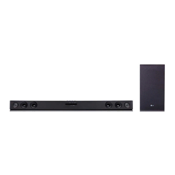
- Page 1 Internal Use Only 2.1 ch Wireless Sound Bar SERVICE MANUAL MODEL: SJ3 (SJ3, SPJ4B-W) CAUTION BEFORE SERVICING THE UNIT, READ THE “SAFETY PRECAUTIONS” IN THIS MANUAL. P/NO : AFN77558553 JANUARY, 2017...
- Page 2 CONTENTS SECTION 1 ..GENERAL SECTION 2 ..CABINET & MAIN CHASSIS SECTION 3 ..ELECTRICAL SECTION 4 ..WIRELESS SUBWOOFER PART...
-
Page 3: Table Of Contents
SECTION 1 GENERAL CONTENTS ESD PRECAUTIONS ............................1-3 WIRELESS SUBWOOFER CONNECTION ....................... 1-4 HIDDEN KEY MODE ............................1-5 ESS / EQ PROGRAM UPDATE GUIDE ......................1-6 SPECIFICATIONS ............................. 1-7... -
Page 4: Esd Precautions
ESD PRECAUTIONS Electrostatically Sensitive Devices (ESD) Some semiconductor (solid state) devices can be damaged easily by static electricity. Such components commonly are called Electrostatically Sensitive Devices (ESD). Examples of typical ESD devices are integrated circuits and some field-effect transistors and semiconductor chip components. The following techniques should be used to help reduce the incidence of component damage caused by static electricity. -
Page 5: Wireless Subwoofer Connection
WIRELESS SUBWOOFER CONNECTION LED indicator of wireless subwoofer Note : • It takes a few seconds (and may take longer) for the main unit and the subwoofer to communicate with LED Color Status each other and make sounds. Green • The closer the main unit and the subwoofer, the Attempting to make connection. -
Page 6: Hidden Key Mode
HIDDEN KEY MODE HIDDEN MODE KEYS Option EDIT Main unit 'VOL-' + Remote Control 'NIGHT ON' Initialize Main unit 'VOL-' + Remote Control 'ASC' Version Check Main unit 'VOL-' + Remote Control 'Play' Clip Off Clip On Main unit 'VOL-' + Remote Control 'Function' Clip On Gain Monitoring Enter : Main unit 'VOL-' + Remote Control 'B.Skip' Wireless RF Change... -
Page 7: Ess / Eq Program Update Guide
- Do format USB Memory to FAT32 File system. - USB : Update fi le exist only in the USB Memory stick. Ex ) SJ3 : E:\DSP_SJ3_*.rom (if USB driver is E:\) E:\EQ_PRG.BIN (if USB driver is E:\) Wireless Tx ... -
Page 8: Specifications
SPECIFICATIONS • GENERAL Power requirements Refer to main label. Power consumption Refer to main label. Networked standby : 0.5 W (If all network ports are activated.) Dimensions (W x H x D) Approx. 950 mm x 71 mm x 47 mm Operating temperature 5 °C to 35 °C Operating humidity... - Page 10 SECTION 2 CABINET & MAIN CHASSIS CONTENTS EXPLODED VIEWS ............................2-3 1. MAIN SET SECTION ..........................2-3 2. WIRELESS SUBWOOFER SECTION ...................... 2-5 3. PACKING ACCESSORY SECTION ......................2-7...
-
Page 12: Exploded Views
EXPLODED VIEWS 1. MAIN SET SECTION NOTES) THE EXCLAMATION POINT WITHIN AN EQUILATERAL TRIANGLE IS INTENDED TO ALERT THE SERVICE PERSONNEL TO THE PRESENCE OF IMPORTANT SAFETY INFORMATION IN SERVICE A44B LITERATURE. SPK703 CABLE2 SMPS CABLE3 A44A MAIN FRONT CABLE1 SPK704 WIRELESS... -
Page 13: Wireless Subwoofer Section
2. WIRELESS SUBWOOFER SECTION NOTES) THE EXCLAMATION POINT WITHIN AN EQUILATERAL TRIANGLE IS INTENDED TO ALERT THE SERVICE PERSONNEL TO THE PRESENCE OF IMPORTANT SAFETY INFORMATION IN SERVICE LITERATURE. A900 A900W SMPS & AMP A45W A54W 300W... -
Page 14: Packing Accessory Section
3. PACKING ACCESSORY SECTION 801 Owner’s manual 835 Wall bracket 808 Batteries (2) 900 Remote control 803 Packing, Main 804 Bag 802 Box... - Page 16 SECTION 3 ELECTRICAL CONTENTS ONE POINT REPAIR GUIDE ..........................3-2 1. NO POWER PROBLEM (PVDD) ......................3-2 2. POWER ON ERROR ..........................3-3 3. NO SOUND (PORTABLE FUNCTION) ....................3-4 4. NO WIRELESS ............................3-5 5. NO BLUETOOTH ............................ 3-6 6.
-
Page 17: One Point Repair Guide
ONE POINT REPAIR GUIDE 1. NO POWER PROBLEM (PVDD) No power problem occurs when you power on the unit. 1-1. Solution Replace SMPS board. 1-2. How to troubleshoot (Countermeasure) 1) Check the PVDD voltage 24.5 V at pin4, 5, 6. When you check the no power at this point, then replace SMPS board. -
Page 18: Power On Error
ONE POINT REPAIR GUIDE 2. POWER ON ERROR No display or Not working. 2-1. IC608 (NO 12 VA) 1) Check 12 VA at L604. 2) If 12 VA is not checked at the point, then find 24.5 V at pin2 of IC608. 3) 1), 2) is NG. -
Page 19: Sound (Portable Function)
ONE POINT REPAIR GUIDE 3. NO SOUND (PORTABLE FUNCTION) 3-1. Solution Replace IC508 or portable jack (JK500). 3-2. How to troubleshoot (Countermeasure) 1) Please check the soldering status of JK500. 2) Please check L507, L508 (PORT_L, PORT_R signal) of portable jack (JK500). If you can’t find input signal, replace JK500. -
Page 20: Wireless
ONE POINT REPAIR GUIDE 4. NO WIRELESS 4-1. Solution Replace WIC500 on MAIN board.(No 3.3 V) 4-2. How to troubleshoot (Countermeasure) 1) Please check externally status of Wireless cable connection on your eyes. (at CN503 and Wireless module) 2) Please check 3.3 V of WL_3V3 (at WL501). If 3.3 V is ok at WL501, please check SPI signal (WL_SPI_CS/D0/WP/DI/CLK) of WIC500 (pin1, 2, 3, 5, 6). -
Page 21: Bluetooth
ONE POINT REPAIR GUIDE 5. NO BLUETOOTH 5-1. Solution Replace IC501 on MAIN board.(No 3.3 V) 5-2. How to troubleshoot (Countermeasure) 1) Please check externally status of Bluetooth cable connection on your eyes.(at CN504 and Bluetooth module) 2) Please check 3.3 V at L509. If 3.3 V is OK at L509, please check BT_RST, BT_CLK, BT_DAT, UART_RX, UART_TX of IC501 (pin27, 23, 24, 67, 68). -
Page 22: Sound (Optical)
ONE POINT REPAIR GUIDE 6. NO SOUND (OPTICAL) 6-1. Solution Replace IC501 on MAIN board. 6-2. How to troubleshoot (Countermeasure) 1) Please check 3.3 V of 3.3VA at R549. If you can check 3.3 V, please confirm OPT_IN signal (R528) when optical mode. 2) In spite of process 1), set has abnormal output, then replace IC501. -
Page 23: D(Dc) Protection
ONE POINT REPAIR GUIDE 7. D(DC) PROTECTION 7-1. Solution Replace IC703 (AMP IC) on MAIN board. 7-2. How to troubleshoot (Countermeasure) 1) Check DC Voltage of speaker out FL+/- (CN703 pin1, 2), FR+/- (CN704 pin1, 3). 2) Check resistor crack, cold solder of IC501 out (R570 ~ R573). 3) If IC501 out is ok and speaker out (FL+/-, FR+/-) has DC Voltage, Replace IC703 (AMP IC) on MAIN bottom board. -
Page 24: S(Shut Down) Protection
ONE POINT REPAIR GUIDE 8. S(SHUT DOWN) PROTECTION 8-1. Solution Replace IC703 (AMP IC) on MAIN board. 8-2. How to troubleshoot (Countermeasure) 1) Check PVDD voltage (24 V) of IC703 pin36, 37, 38. - If PVDD voltage has 8.5 V under, refer to “1. NO POWER PROBLEM (PVDD)” on page 3-2. 2) Check GVDD, VDD voltage (12 V) of IC703 pin1, 2. -
Page 25: B(Burnt) Protection
ONE POINT REPAIR GUIDE 9. B(BURNT) PROTECTION 9-1. Solution Replace IC703 (AMP IC) on MAIN board. 9-2. How to troubleshoot (Countermeasure) 1) Check voltage 12 V of IC703 at pin1, if 12 V has problem, refer to “2. POWER ON ERROR” on page 3-3. 2) If 12 V is OK, replace IC703 (AMP IC) on MAIN bottom board. -
Page 26: Waveforms Of Major Check Point
WAVEFORMS OF MAJOR CHECK POINT 1. CRYSTAL 2. FLASH MEMORY FIG 1. X500 (27 MHz) FIG 2. VCC, CS#, CLK, DO 3-11... -
Page 27: Tact Key
3. TACT KEY 1 ~ 1.13 V 0.72 ~ 0.82 V FIG 3-2. Press FUNC Key FIG 3-1. Press Power Key 0.424 ~ 0.485 V FIG 3-3. Press - Key FIG 3-4. Press + Key 3-12... -
Page 28: Remote Control
4. REMOTE CONTROL FIG 4-1. Input Voltage 11 12 FIG 4-2. Low Timing Item Measured Spec. IR Receiver Spec: Input Level 3.3 V 2.7 ~ 5.5 V “ Low” Timing 4.4 ms 3.6 ms ~ 5.04 ms “ High” Timing 4.48 ms 4.08 ms ~ 5.04 ms FIG 4-3. -
Page 29: Optical
5. OPTICAL FIG 5-1. SPDIF_IN FIG 5-2. OPT_DET 3-14... -
Page 30: Portable
6. PORTABLE 1 1 .27 Vrms FIG 6. Analog Input Voltage 3-15... -
Page 31: Audio Pwm
7. AUDIO PWM FL+ FL- FR+ FR- 384.14 kHz 384.17 kHz FIG 7-1. Front L FIG 7-2. Front R 3-16... -
Page 32: Wiring Diagram
WIRING DIAGRAM FRONT (CEM-1 1.6T 128.5x55) Array size: 257x128 CN300 Powercord 10P FFC CN502 MAIN SMPS (FR4 Epoxy 4layer 1.2T 234x59.5) (FR1 1layer 1.6T 167x59.5) Array size: 242x133 Array size: 167x147 6P BtoB CN504 CN503 10P FFC 26P FFC Harness Harness SPK(FL) SPK(FR) -
Page 33: Block Diagrams
BLOCK DIAGRAMS 1. SYSTEM BLOCK DIAGRAM 27 MHz BT_UART Bluetooth AMP_PROTECT/FAULT/PDN Module DC_PROTECTION BT_RST/CLK / DAT Audio Optical In FL_OUT_P/N, FR_OUT_P/N SPDIF /OPT_DET Potable In Potable_L / R, Potable_DET USB+/- I2S(BCK/LRCK/ADATA2) Wireless Wireless WL_MUT/RST/INT MAIN DSP Module Woofer MSG_RDY/I2C Serial Flash 1 MB Front PCB IR -Receiver... -
Page 34: Power Block Diagram
2. POWER BLOCK DIAGRAM SMPS PVDD (24.5V) Q602 Switching +12 V 10 mA P_CTRL IC611 USB5V 500 mA Switch IC602 VD33ADAC 10 mA VD33AADC 5 mA VD33ADAC IC609 IC608 IC605 5.1 VA 1.35 V VD13 350 mA 12 VA DCDC Duel -DCDC DCDC [2 A]... -
Page 35: Circuit Voltage Chart
CIRCUIT VOLTAGE CHART 1. CONNECTORS Mearsured Voltage Part Designator Description Pin Number Voltage Spec Remark (Main) 12 V 11.87 V CN501 Connector,FFC/FPC/PIC 5.13 V DISPLAY JIG 3.3 V 3.32 V VCC_3.3V 3.29 V Main Board CN502 Connector, FFC FRONT Interface 3.3 VA 3.3 V CN503... -
Page 36: Others
2. OTHERS Designator Description Pin Number Voltage Spec. Measured Voltage Main Board C502 Capacitor,AL,Chip 16 V 3.37 V C744 Capacitor,AL,Chip 25.7 V(PVDD) 25.64 V C747 Capacitor,AL,Chip 25.7 V(PVDD) 25.63 V CN503 Connector,FFC 3.3 V(Wireless) 3.37 V 7, 18, 25, 54, 61, 71, 81, 82 VD33 3.34 V VD33PLL... -
Page 37: Printed Circuit Board Diagrams
PRINTED CIRCUIT BOARD DIAGRAMS 1. SMPS P. C. BOARD DIAGRAM (TOP VIEW) NOTE) Warning Parts that are critical with respect to risk of fire or electrical shock. (BOTTOM VIEW) 3-27 3-28... -
Page 38: Main P. C. Board Diagram
2. MAIN P. C. BOARD DIAGRAM (TOP VIEW) (BOTTOM VIEW) 3-29 3-30... -
Page 39: Front P. C. Board Diagram
3. FRONT P. C. BOARD DIAGRAM (TOP VIEW) (BOTTOM VIEW) 3-31 3-32... - Page 40 SECTION 4 WIRELESS SUBWOOFER PART CONTENTS ONE POINT REPAIR GUIDE ..........................4-2 1. POWER ON ERROR ..........................4-2 2. WIRELESS CONNECTION ........................4-4 WAVEFORMS OF MAJOR CHECK POINT ...................... 4-5 1. CRYSTAL ..............................4-5 2. FLASH MEMORY ........................... 4-5 3. VOLTAGE ............................... 4-6 4.
-
Page 41: One Point Repair Guide
ONE POINT REPAIR GUIDE 1. POWER ON ERROR Fundamental power check points. 1-1. 12 V 1) Check 12 V at WL708. 2) If 12 V is not checked at the point, then find PVDD at pin7 of WIC704. 3) 1), 2) is NG Replace WIC704. If you can’t check PVDD voltage, then replace the PCB board. - Page 42 ONE POINT REPAIR GUIDE POWER ON ERROR Fundamental power check points. 1-3. 3.3 VA 1) Check 3.3 VA at pin1 of WIC703. 2) Check 3.3V_PWM at pin6 of WIC703. 3) 1), 2) is NG Replace WIC703. If you can’t check PVDD voltage, then replace the PCB board. WIC703 WIC703 <...
-
Page 43: Wireless Connection
ONE POINT REPAIR GUIDE 2. WIRELESS CONNECTION Wireless connection malfunction. 2-1. 3.3 VA 1) Check 3.3 VA at WFB604. 2-2. Connection 1) Wireless module connection closely. 2) Implement Wireless Factory Reset. MAIN SET : Soundbar vol MIN and push Mute key (sustain 3 ~ 5 seconds). ... -
Page 44: Waveforms Of Major Check Point
WAVEFORMS OF MAJOR CHECK POINT 1. CRYSTAL FIG 1. WX601 (24.576 MHz) 2. FLASH MEMORY FIG 2. VCC, CS#, CLK, DO... -
Page 45: Voltage
3. VOLTAGE FIG 3-2. Woofer 12 VA FIG 3-1. Woofer PVDD FIG 3-3. Woofer 3.3 VA FIG 3-4. Woofer 3.3V_PWM... -
Page 46: Amp Voltage
4. AMP VOLTAGE FIG 4-2. AMP_12V FIG 4-1. AMP PVDD... -
Page 47: Pwm
5. PWM FIG 5-2. Woofer PWM SW- Signal FIG 5-1. Woofer PWM SW+ Signal... -
Page 48: Led
6. LED FIG 6-2. Pairing On Status Green LED FIG 6-1. Pairing Off Status Red LED... - Page 49 4-10...
-
Page 50: Wiring Diagram
WIRING DIAGRAM 2P, 3.96 mm ST, Non Lock SMD Wireless 26P, 0.5 mm ST, Non Lock SMD 2P, 3.96 mm ST, Non Lock , SMD Power Bottom Bottom FFC C Harness Harness 4-11 4-12... -
Page 51: Block Diagram
BLOCK DIAGRAM Wireless LED (RED, GREEN) Wireless AMP_PDN AMP_SD PAIRING R R eset KEY SW+/SW- PWM IC 4-13 4-14... -
Page 52: Circuit Voltage Chart
CIRCUIT VOLTAGE CHART Location No. Description Pin Number Specifi cation Real Value (#1, #2) VDD _IO: VDD_IO: 3.37 V 3.37 V #17, 43, 52 2.97 V ~ 3.63 V VDD_CORE: VDD_CORE: 1.08 V WIC601 Sound/Audio Pro- 1.27 V 1.27 V #6, 25, 63 ~ 1.32 V cessor... -
Page 53: Printed Circuit Board Diagrams
PRINTED CIRCUIT BOARD DIAGRAMS 1. WOOFER SMPS & AMP P. C. BOARD (TOP VIEW) (BOTTOM VIEW) NOTE) Warning Parts that are critical with respect to risk of fire or electrical shock. 4-17 4-18...
Need help?
Do you have a question about the SJ3 and is the answer not in the manual?
Questions and answers