
Related Manuals for LG SJ2


Summary of Contents for LG SJ2
- Page 1 Internal Use Only Wireless Sound Bar SERVICE MANUAL MODEL: SJ2 (SJ2, SPJ2B-W) CAUTION BEFORE SERVICING THE UNIT, READ THE “SAFETY PRECAUTIONS” IN THIS MANUAL. P/NO : AFN78037532 JUNE, 2017...
- Page 2 CONTENTS SECTION 1 ..SUMMARY SECTION 2 ..CABINET & MAIN CHASSIS SECTION 3 ..ELECTRICAL SECTION 4 ..WIRELESS SUBWOOFER PART...
-
Page 3: Table Of Contents
SECTION 1 SUMMARY CONTENTS PRODUCT SAFETY SERVICING GUIDELINES FOR AUDIO PRODUCTS ............ 1-3 SERVICING PRECAUTIONS ..........................1-4 • GENERAL SERVICING PRECAUTIONS • INSULATION CHECKING PRODEDURE • ELECTROSTATICALLY SENSITIVE (ES) DEVICES NAME OF EACH COMPONENT ........................1-5 WIRELESS SUBWOOFER CONNECTION ....................... 1-6 HIDDEN KEY MODE ............................ -
Page 4: Product Safety Servicing Guidelines For Audio Products
When servicing this product, under no circumstances should the original design be modified or altered without permission from LG Corporation. All components should be replaced only with types identical to those in the original circuit and their physical location, wiring and lead dress must conform to original layout upon completion of repairs. -
Page 5: Servicing Precautions
SERVICING PRECAUTIONS CAUTION: Before servicing the Audio products covered by this Electrostatically Sensitive (ES) Devices service data and its supplements and addends, read and fol- Some semiconductor (solid state) devices can be damaged low the SAFETY PRECAUTIONS. easily by static electricity. Such components commonly are NOTE: if unforeseen circumstances create conflict between called Electrostatically Sensitive (ES) Devices. -
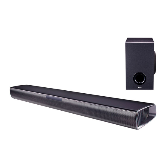
Page 6: Name Of Each Component
NAME OF EACH COMPONENT • Front Panel A Standby LED (Red) Standby LED (Red) D The buttons are located on the rear. The buttons are located on the rear. Function LED (White) Remote sensor • Rear Panel A o/p (Volume) : Adjusts volume level (USB) : Connect to a USB device. -
Page 7: Wireless Subwoofer Connection
WIRELESS SUBWOOFER CONNECTION LED indicator of wireless subwoofer Note : • It takes a few seconds (and may take longer) for the main unit and the subwoofer to communicate LED Color Status with each other and make sounds. Green • The closer the main unit and the wireless subwoofer, Attempting to make connection. -
Page 8: Hidden Key Mode
HIDDEN KEY MODE HIDDEN MODE KEYS Version Check Main unit ‘– (Volume)’ + Remote control ‘ll (Play/Pause)’ Clip On/Off Main unit ‘– (Volume)’ + Remote control ‘F’ Wireless RF Main unit ‘– (Volume)’ + Remote control ‘B.Skip’ Sound BYPASS Main unit ‘– (Volume)’ + Remote control ‘AUTO POWER OFF’ ON: Press and hold ‘DRC ON’... -
Page 9: Software Update Guide
1. Preparation - Remote control. - Do format USB Memory to FAT32 File system. - USB : Update fi le exist only in the USB Memory stick. Ex) SJ2 : MCS : E:\SJ2_201701250.bin (if USB driver is E:\) Wireless Tx ... -
Page 10: Specifications
SPECIFICATIONS GENERAL Power requirements Refer to the main label. Power consumption Refer to the main label. Dimensions (W x H x D) Approx. 660 mm x 56 mm x 99 mm with foot Operating temperature 5 °C to 35 °C Operating humidity 5 % to 90 % Bus Power Supply... - Page 11 1-10...
- Page 12 SECTION 2 CABINET & MAIN CHASSIS CONTENTS DISASSEMBLY INSTRUCTIONS ........................2-2 1. HOW TO DISASSEMBLE THE MAIN UNIT ..................... 2-2 2. HOW TO DISASSEMBLE THE SUBWOOFER ..................2-6 EXPLODED VIEWS ............................2-9 1. MAIN UNIT SECTION ..........................2-9 2. WIRELESS SUBWOOFER SECTION ....................2-11 3.
-
Page 13: Disassembly Instructions
DISASSEMBLY INSTRUCTIONS 1. HOW TO DISASSEMBLE THE MAIN UNIT ※ Before begin, position the Main Unit upside down. 1-1. Case Bottom Assembly 1) Remove the 19 screws. 2) Remove the Case Bottom Assembly. Figure 1-1... -
Page 14: How To Disassemble The Main Unit
HOW TO DISASSEMBLE THE MAIN UNIT 1-2. Main Chassis Assembly 1) Disconnect the 5 cables from the Main PCB Assembly and SMPS PCB Assembly. Figure 1-2 (1) 2) Remove the 2 screws. 3) Remove the Main Chassis Assembly. (Main Chassis + PCBA) Figure 1-2 (2) - Page 15 HOW TO DISASSEMBLE THE MAIN UNIT 1-2-1. LED PCB Assembly 1) Disconnect the cable from the Main PCB Assembly. 2) Remove the 2 screws. 3) Remove the LED PCB Assembly. Figure 1-2-1 1-2-2. Main PCB Assembly and SMPS PCB Assembly 1) Remove the 2 screws.
- Page 16 HOW TO DISASSEMBLE THE MAIN UNIT 1-3. Speaker Chamber Assembly and BT module 1) Remove the Speaker Chamber Assembly. 2) Remove the BT module. Figure 1-3...
- Page 17 2. HOW TO DISASSEMBLE THE SUBWOOFER 2-1. Rear Panel Assembly 1) Remove the 11 screws. Figure 2-1 (1) 2) Pull out the Rear Panel Assembly and disconnect the Speaker cable. Figure 2-1 (2)
-
Page 18: How To Disassemble The Subwoofer
HOW TO DISASSEMBLE THE SUBWOOFER 2-2. SMPS & AMP PCB Assembly 1) Disconnect the Power inlet socket cable. Figure 2-2 (1) 2) Remove the 5 screws. 3) Remove the SMPS & AMP PCB Assembly. Figure 2-2 (2) -
Page 20: Exploded Views
EXPLODED VIEWS 1. MAIN UNIT SECTION NOTES) THE EXCLAMATION POINT WITHIN AN EQUILATERAL TRIANGLE IS INTENDED TO ALERT THE SERVICE PERSONNEL TO THE PRESENCE OF IMPORTANT SAFETY INFORMATION IN SERVICE LITERATURE. WIRELESS CABLE4 MAIN CABLE2 SMPS CABLE1 271R CABLE3 CABLE4 271L 2-10... -
Page 21: Wireless Subwoofer Section
2. WIRELESS SUBWOOFER SECTION NOTES) THE EXCLAMATION POINT WITHIN AN EQUILATERAL TRIANGLE IS INTENDED TO ALERT THE SERVICE PERSONNEL TO THE PRESENCE OF IMPORTANT SAFETY INFORMATION IN SERVICE LITERATURE. A900 A901 300W A54W WIRELESS A45W SMPS & AMP 2-11 2-12... -
Page 22: Packing Accessory Section
3. PACKING ACCESSORY SECTION Owner’s manual Optical cable Batteries Wall bracket Remote control Screws 804 Bag Packing, Main 802 Box 2-13... - Page 23 2-14...
- Page 24 SECTION 3 ELECTRICAL CONTENTS ONE POINT REPAIR GUIDE ..........................3-2 1. NO POWER PROBLEM ......................... 3-2 2. SPEAKER NO AUDIO OUTPUT ......................3-3 3. USB NO DETECT ........................... 3-4 ELECTRICAL TROUBLESHOOTING GUIDE ....................3-5 1. SMPS POWER CIRCUIT ........................3-5 2.
-
Page 25: One Point Repair Guide
ONE POINT REPAIR GUIDE 1. NO POWER PROBLEM No power problem occurs when you power on the unit. 1-1. Solution Replace XL301, IC307, IC305. 1-2. How to troubleshoot (Countermeasure) 1) Check XL301(Crystal). If it does not oscillate, replace XL301. 2) Check IC307(Reset IC). -
Page 26: Speaker No Audio Output
ONE POINT REPAIR GUIDE 2. SPEAKER NO AUDIO OUTPUT No audio output problem occurs when you power on the unit. 2-1. Solution Replace IC500. 2-2. How to troubleshoot (Countermeasure) 1) Check L504, L505. If it is not appear 21 V, please check the switch power supply board. 2) 21 V the voltage is normal, please check IC500 pin20, 21, 22 I2S signal. -
Page 27: Usb No Detect
ONE POINT REPAIR GUIDE 3. USB NO DETECT When USB insert, USB no detect on the unit. 3-1. Solution Replace IC302. 3-2. How to troubleshoot (Countermeasure) 1) Please check IC302. pin1 : 5 V 2) If it is not OK, replace IC302. 3-3. -
Page 28: Electrical Troubleshooting Guide
ELECTRICAL TROUBLESHOOTING GUIDE 1. SMPS POWER CIRCUIT No 23 V F900 normal? Replace F900 (same fuse). Replace NTC900. NTC900 normal? Replace BD900. BD900 normal? Check or replace IC900. Is the Vcc (16 V~17 V) IC900 normal? supplied to IC900 pin6? The IC902 is short. - Page 29 ELECTRICAL TROUBLESHOOTING GUIDE SMPS POWER CIRCUIT No 3.3 VA Check FB100 voltage 23 V. Check SMPS. Check IC100. Check IC100 voltage 5 V. Replace IC101. Check IC101 voltage 3.3 V. Check 3.3 VA network, the device a short circuit will cause no output. No 1.2 VA Check FB100 voltage 21 V.
-
Page 30: Key Part
ELECTRICAL TROUBLESHOOTING GUIDE 2. KEY PART Key part Replace the cables. Check CN800 pin3, 4 voltage. Check the connecting cables. Check R428 Pull-up resistors. Replace the related part. Check TA800, TA801, TA802, TA803. Check R800, R801, R802, R803. -
Page 31: Power Amp Part
ELECTRICAL TROUBLESHOOTING GUIDE 3. POWER AMP PART Power AMP part Refer to The main power of 21 V. Power part troubleshooting. Check input power of IC500 pin2, 3, 34, 35, 40, 41, 44, 45 21 V input. Check IC500 pin13, 27 Check IC104. -
Page 32: Portable Function
ELECTRICAL TROUBLESHOOTING GUIDE 4. PORTABLE FUNCTION Portable function Check JK300. Replace the related part. Check IC301 pin13, 14 Check IC301 pin3: 5 V, pin4 3.3 V. input waveform. Refer to Power part troubleshooting. Check IC301 pin7, 8, 9 SDOUT. Check IC301. -
Page 33: Optical Function
ELECTRICAL TROUBLESHOOTING GUIDE 5. OPTICAL FUNCTION Optical function Replace the related part. Check JK301. Check FB300, R300. Check C302 3.3 V voltage. Refer to Power part troubleshooting. Check IC300 pin6 Check C321. input waveform. Replace the related part. Refer to Power part troubleshooting. -
Page 34: Usb Part
ELECTRICAL TROUBLESHOOTING GUIDE 6. USB PART Refer to Turn on USB Power part troubleshooting. Check IC302 pin1 Check IC302 5.2 V input. pin5 5.2 V input. Check JK302 pin1 5.2 V. Check Check JK302 pin2(D-), pin3 (D+). Reading OK. Check IC305 pin62, 64. 3-11... -
Page 35: Waveforms Of Major Check Point
WAVEFORMS OF MAJOR CHECK POINT 1. CRYSTAL FIG 1-1. XL301 (24 MHz) FIG 1-2. XL300 (24.576 MHz) 3-12... -
Page 36: Amp Ic
2. AMP IC AMP_TSDO AMP_BCK AMP_LRCK FIG 2. IC500 pin20, 21, 22 3-13... -
Page 37: Reset Ic
3.3 VA 3. RESET IC 3.3 VA 1.2 VA RESET 3.08 V FIG 3-1. IC307 pin2 FIG 3-2. IC307 pin2 3-14... -
Page 38: Amp Fault
4. AMP FAULT FIG 4. IC500 pin14 3-15... - Page 39 3-16...
-
Page 40: Wiring Diagram
WIRING DIAGRAM SMPS MAIN 3-17 3-18... -
Page 41: Block Diagram
BLOCK DIAGRAM BT Internal Antenna UART(Single) control I2C / RST / PWDN 8 Ω 30 W THD 10 % BT Module DATA0(P124) MCLK DATA PWR AMP CRYSTAL LRCK 24.576 MHz SPDIF_RX BK3V3 LRCK IC500 SPIDF-IN IC300 BK5 V 8 Ω 30 W MCLK THD 10 % OPTICAL... -
Page 42: Circuit Voltage Chart
CIRCUIT VOLTAGE CHART Location No. Pin Number Specifi cation Real Value MAIN Board 3.1-3.6 V 3.3 V BK33 3.1-3.6 V 3.3 V USB IN_LED 0-3.6 V 0-3.2 V CN300 Audio IN_LED 0-3.6 V 0-3.2 V BT_LED 0-3.6 V 0-3.2 V Optical_LED 0-3.6 V 0-3.2 V... -
Page 43: Printed Circuit Board Diagrams
PRINTED CIRCUIT BOARD DIAGRAMS 1. SMPS P. C. BOARD DIAGRAM (TOP VIEW) (BOTTOM VIEW) NOTE) Warning Parts that are critical with respect to risk of fire or electrical shock. 3-23 3-24... -
Page 44: Main P. C. Board Diagram
2. MAIN P. C. BOARD DIAGRAM (TOP VIEW) (BOTTOM VIEW) 3-25 3-26... -
Page 45: Key P. C. Board Diagram
3. KEY P. C. BOARD DIAGRAM 4. LED P. C. BOARD DIAGRAM 3-27 3-28... - Page 46 SECTION 4 WIRELESS SUBWOOFER PART CONTENTS ELECTRICAL TROUBLESHOOTING GUIDE ....................4-2 1. SMPS POWER CIRCUIT ........................4-2 2. LED PART ............................... 4-4 3. POWER AMP PART ..........................4-5 WAVEFORMS OF MAJOR CHECK POINT ...................... 4-6 1. AMP IC ..............................4-6 WIRING DIAGRAM ............................
-
Page 47: Electrical Troubleshooting Guide
ELECTRICAL TROUBLESHOOTING GUIDE 1. SMPS POWER CIRCUIT No 24.7 V F900 normal? Replace F900 (same fuse). Replace NTC900. NTC900 normal? Replace BD900. BD900 normal? Is the Vcc (12 V~16 V) Check or replace IC900. supplied to IC900 pin6? Replace IC901, IC902. IC901, IC902 normal? Check IC901, IC902 network, the device a short circuit will cause no output. - Page 48 ELECTRICAL TROUBLESHOOTING GUIDE SMPS POWER CIRCUIT No 3.3 VA Check C940 voltage 24 V. Check SMPS. Check IC300. Check IC300 voltage 3.3 V. Check Q203. Check Q203 voltage 3.3 V. Check U201 pin8, 31 Check U201. voltage 3.3 V. Check 3.3 VA network, the device a short circuit will cause no output.
-
Page 49: Led Part
ELECTRICAL TROUBLESHOOTING GUIDE 2. LED PART LED part Check SMPS. Check MD200 pin1 Check C940 voltage 3.3 V. voltage 24 V. Replace IC300. Replace LD202. Check LD202. Replace Wireless module. Check Wireless module. Check LD202 network, the device a short circuit will cause no output. -
Page 50: Power Amp Part
ELECTRICAL TROUBLESHOOTING GUIDE 3. POWER AMP PART Power AMP part The sub power of 24 V. Refer to No 24.7 V. Check Q300 pin5, 6, 7, 8 24.7 V output. Check U201 pin8, 31 Check Q203, Q303. 3.3 V input. Check I2S signal input U201 pin9, 10, 11. -
Page 51: Waveforms Of Major Check Point
WAVEFORMS OF MAJOR CHECK POINT 1. AMP IC AMP_SDATA AMP_BCLK AMP_LRCIN FIG 1. U201 pin9, 10, 11... -
Page 52: Wiring Diagram
WIRING DIAGRAM... -
Page 53: Block Diagram
BLOCK DIAGRAM Internal Antenna SW-TACK LRCK TAS5538 ABCK 3 Ω PWR AMP Subwoofer SDOUT 100 W(10 %) U201 VOLUME MCLK LED-W Magnat SUB: 140 W 10 % 31 V Magnat SUB: 105 W 10 % 25.7 V SUB Power Board fixed AC power cord 115 W PSU 26 V... -
Page 54: Circuit Voltage Chart
CIRCUIT VOLTAGE CHART Location No. Pin Number Specifi cation Real Value SUB- 0~12.33 V 12.33 V CN201 SUB+ 0~12.33 V 12.33 V 3.1-3.5 V 3.28 V 3.1-3.5 V 3.28 V CN203 REST 3.1-3.5 V 3.27 V 3.3V 3.1-3.5 V 3.31 V 4-11 4-12... -
Page 55: Printed Circuit Board Diagram
PRINTED CIRCUIT BOARD DIAGRAM 1. SMPS & AMP P. C. BOARD DIAGRAM NOTE) Warning Parts that are critical with respect to risk (TOP VIEW) (BOTTOM VIEW) of fire or electrical shock. 4-13 4-14...
Need help?
Do you have a question about the SJ2 and is the answer not in the manual?
Questions and answers