
Subscribe to Our Youtube Channel
Related Manuals for ozQRP MST3


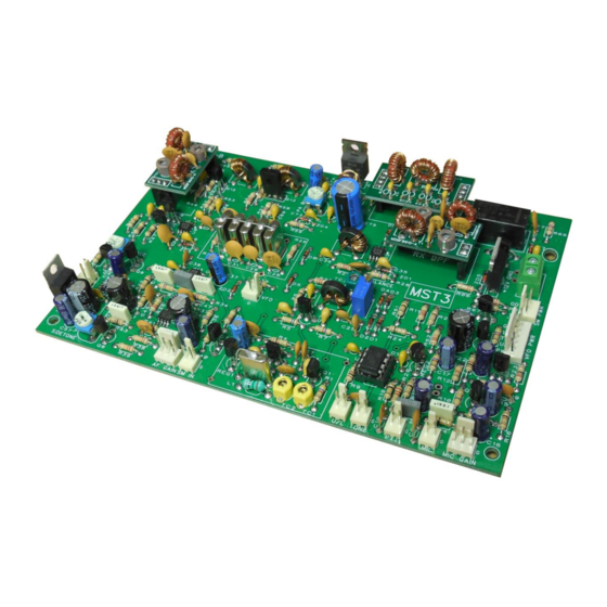
Summary of Contents for ozQRP MST3
- Page 1 MST3 TRANSCEIVER OARD ONSTRUCTION AND OPERATION ANUAL MST3 Construction and Operation Manual – Issue 1 Page 1...
-
Page 2: Table Of Contents
11 Enclosure ................................. 46 11.1 Front Panel ..................................46 11.2 Rear Panel ..................................46 11.3 Mounting the PCB ................................47 12 Wiring up ................................. 48 12.1 general ....................................48 12.2 Headers ....................................48 MST3 Construction and Operation Manual – Issue 1 Page 2... - Page 3 Introduction ................................58 14.3.2 Operation ................................. 58 14.4 CW Mode ..................................... 59 14.4.1 Introduction ................................59 14.4.2 Operation ................................. 59 14.5 Test Tones ..................................60 14.6 Entering a Callsign................................60 MST3 Construction and Operation Manual – Issue 1 Page 3...
- Page 4 Figure 14 LPF overlay ..............................43 Figure 15 Completed LPF ............................43 Figure 16 MST3 in an enclosure ..........................46 Figure 17 MST3 board and rear panel ........................47 Figure 18 Wiring diagram ............................49 Figure 20 Carrier frequency and crystal filter relationship ................. 56 List of Tables Table 1 BPF components ............................
-
Page 5: Introduction
With the addition of a VFO, an enclosure and a hand full of parts you have a complete and working SSB transceiver. Full kits of parts for the MST3 transceiver board and plug-in band filter sets are available from www.ozQRP.com. - Page 6 17. Connectors for optional LED S meter or a simple front panel LED transmit power and modulation indicator. 18. PCB size 165mm x 110mm. Mounting holes 157mm x 83mm. 19. High quality double sided PCB with groundplane, solder mask and silk screen. MST3 Construction and Operation Manual – Issue 1 Page 6...
-
Page 7: Block Diagram
LOCK IAGRAM Figure 1 MST3 Block diagram MST3 Construction and Operation Manual – Issue 1 Page 7... -
Page 8: Circuit Description
As a result a signal is now output on the secondary of T1, which is a double sideband suppressed carrier waveform. MST3 Construction and Operation Manual – Issue 1 Page 8... -
Page 9: Crystal Filter
50 ohm load. The waveform from Q14 can be high in harmonics and so a 7 pole low pass filter is included to reduce the level of harmonic and other spurious energy to an acceptable level. MST3 Construction and Operation Manual – Issue 1 Page 9... -
Page 10: Power Supply And Rx/Tx Switching
10MHz BFO signal to produce an audio output. The BFO is adjusted slightly above the crystal filter response for LSB and slightly below the crystal filter response for USB detection. MST3 Construction and Operation Manual – Issue 1 Page 10... -
Page 11: Audio Power Amplifier
Capacitor C56 stores the charge in between positive cycles to avoid Q9 turning off during negative peaks and causing distortion. For such a simple circuit the dynamics are very good and make a great addition to the receiver. MST3 Construction and Operation Manual – Issue 1 Page 11... -
Page 12: Intelligent Tone Module
3.11.1 O VERVIEW The Intelligent Tone Module (ITM) is based around an ATtiny85 microcontroller incorporating a high speed pulse width modulation (PWM) generator. The ITM has a central role in the MST3 and performs the following functions: Tone generator for CW operation. The keyed tone bursts are shaped to minimise keying clicks. - Page 13 PTT line. At power up the ITM emits two short beeps to signal a successful boot up. The ITM is supplied with +5V by a 78L05 regulator. MST3 Construction and Operation Manual – Issue 1 Page 13...
-
Page 14: Figure 2 Carrier Oscillator
Figure 2 Carrier oscillator MST3 Construction and Operation Manual – Issue 1 Page 14... -
Page 15: Figure 3 Balanced Modulator
Figure 3 Balanced Modulator MST3 Construction and Operation Manual – Issue 1 Page 15... -
Page 16: Figure 4 Crystal Filter
Figure 4 Crystal Filter MST3 Construction and Operation Manual – Issue 1 Page 16... -
Page 17: Figure 5 Transmit Mixer
Figure 5 Transmit mixer MST3 Construction and Operation Manual – Issue 1 Page 17... -
Page 18: Figure 6 Power Amplifier And Rx/Tx Switching
Figure 6 Power amplifier and RX/TX switching MST3 Construction and Operation Manual – Issue 1 Page 18... -
Page 19: Figure 7 Receive Mixer
Figure 7 Receive mixer MST3 Construction and Operation Manual – Issue 1 Page 19... -
Page 20: Figure 8 Receive Audio
Figure 8 Receive audio MST3 Construction and Operation Manual – Issue 1 Page 20... -
Page 21: Kit Supplied Parts
56K 1/4W 5% R5, R45 100K 1/4W 5% R2, R18, R41 220K 1/4W 5% R35, R37, R64 470K 1/4W 5% 500Ω vertical multi-turn trimpot 20K horizontal trimpot VR2, VR3, VR4 MST3 Construction and Operation Manual – Issue 1 Page 21... - Page 22 2 pin polarised plug + pins 3 pin polarised plug + pins 6 pin polarised plug + pins 8 pin IC socket Crystals 10MHz crystal X1, X2, X3, X4, X5, X6 MST3 Construction and Operation Manual – Issue 1 Page 22...
-
Page 23: Individual Parts List
MLCC 100nF ceramic MLCC 100nF ceramic MLCC 22uF 25V RB electrolytic ceramic disc 100nF ceramic MLCC 100nF ceramic MLCC 47nF polyester MKT 220uF 25V RB electrolytic 100nF polyester MKT MST3 Construction and Operation Manual – Issue 1 Page 23... - Page 24 1/4W 5% 3.3K 1/4W 5% 1/4W 5% 220Ω 1/4W 5% 220K 1/4W 5% 1/4W 5% 4.7K 1/4W 5% 1/4W 5% 1/4W 5% 100Ω 1/4W 5% 330Ω 1/4W 5% 1/4W 5% MST3 Construction and Operation Manual – Issue 1 Page 24...
- Page 25 Microcontroller SA612 RF mixer SA612 RF mixer NE5532 Dual low noise op-amp TDA7052A BTL power audio amp SA612 RF mixer 500 Ω Multi-turn trimpot Horizontal trimpot Horizontal trimpot Horizontal trimpot MST3 Construction and Operation Manual – Issue 1 Page 25...
-
Page 26: Off Board Parts
OARD ARTS The following is a suggested list of parts required to complete the MST3 transceiver board and install in an enclosure. These parts are not included in the kit. This list does not include the VFO, LED S meter or associated parts. -
Page 27: Main Board Construction
7.1 G ENERAL The MST3 is built on a high quality fiberglass PCB. The PCB is double sided with the majority of the tracks on the bottom side with the top side forming a ground plane. To assist construction the component overlay is screen printed on the top side and a solder mask is included to help guard against solder bridges. -
Page 28: Construction Steps
A dot above pin 1 A beveled edge down one side starting at pin 1 and ending at pin 4. A line across the top from pin 1 to pin 8. MST3 Construction and Operation Manual – Issue 1 Page 28... - Page 29 Form the leads before inserting to reduce stress on the body when pulling through the PCB. Cathode (+) end Zener 1N4148 The diodes are identified with a band printed on the case at the Cathode (+) end. 1N4004 MST3 Construction and Operation Manual – Issue 1 Page 29...
- Page 30 30pF carrier balance trimmer is green. Step 6: Trimpots Note that the carrier balance trimpot is a multi-turn vertical mount while the PA bias, AGC and sidetone trimpots are horizontal mount types. MST3 Construction and Operation Manual – Issue 1 Page 30...
- Page 31 Step 8: Connectors The MST3 board utilizes polarized pin headers for most external connections. If preferred the wires may be soldered directly to the PCB, but the connectors make for a professional looking build, plus allow easy disconnection and testing if required. The connectors have a vertical polarizing piece and the connectors are installed with this piece towards the centre of the PCB.
- Page 32 The PCB component overlay has a ‘+’ mark to indicate the hole for the positive lead. MST3 Construction and Operation Manual – Issue 1 Page 32...
- Page 33 10 turn primary. Scrape the enamel off the ends of the wires and tin with solder before installing in the PCB. The winding direction is not important. MST3 Construction and Operation Manual – Issue 1 Page 33...
- Page 34 PCB and sit the toroid so that it rests against the surface of the board. Ensure the two-wire centre tap goes to the middle hole of the T5 component overlay closest to Q14. MST3 Construction and Operation Manual – Issue 1 Page 34...
- Page 35 Install the 78L08 8V regulator (REG1) and 78L05 5V regulator (REG2) as shown on the silkscreen component overlay. It is very important to check that the 78L05 regulator is inserted next to U1. If the 78L08 is installed here, the ITM will be destroyed. MST3 Construction and Operation Manual – Issue 1 Page 35...
- Page 36 Remove the ITM from its protective foam and install in the 8 pin IC socket. Pin 1 is closest to C13. You may need to compress the pins slightly so that they slide easily into the socket. MST3 Construction and Operation Manual – Issue 1 Page 36...
-
Page 37: Figure 9 Component Overlay
Figure 9 Component overlay MST3 Construction and Operation Manual – Issue 1 Page 37... -
Page 38: Band Pass Filters
The TX and RX bandpass filters for each band are identical apart from the number of turns on the coupling winding of T1. This is done to match the different impedance of the TX and RX mixers. Figure 10 BPF schematic Figure 11 Completed BPF MST3 Construction and Operation Manual – Issue 1 Page 38... -
Page 39: Construction
When the second winding is finished cut these ends shorter. That way after scraping off the enamel the windings are easy to identify before inserting in the PCB. MST3 Construction and Operation Manual – Issue 1 Page 39... -
Page 40: Figure 12 Bpf Overlay
Tuned winding only. Note long wire leads. BPF coil Coupling winding wound over bottom section of tuned winding. Coupling winding wires shorter to allow easy identification. Coupling winding Tuned winding MST3 Construction and Operation Manual – Issue 1 Page 40... -
Page 41: Table 1 Bpf Components
10 turns of 0.4mm enameled wire 56pF coupling wound over T1. 170mm long. 82pF 14 turns T37-6 (yellow) core. 0.4mm enameled wire. 220mm long. 40pF trimcap 22pF Table 1 BPF components MST3 Construction and Operation Manual – Issue 1 Page 41... -
Page 42: Low Pass Filter
3. Pins. Break off the required number of pins from the supplied strip and solder in place on the opposite side of the PCB, ensuring they are at right angles to the board. MST3 Construction and Operation Manual – Issue 1 Page 42... -
Page 43: Figure 14 Lpf Overlay
Figure 14 LPF overlay Figure 15 Completed LPF MST3 Construction and Operation Manual – Issue 1 Page 43... -
Page 44: Table 2 Lpf Components
T37-6 (yellow) core. 13 turns of 0.4mm enameled wire. 220mm long. enameled wire. 220mm long. 330pF (331) 180pF (181) T37-6 (yellow) core. 14 turns of 0.4mm enameled wire. 220mm long. Table 2 LPF components MST3 Construction and Operation Manual – Issue 1 Page 44... -
Page 45: Adding Avfo
The VFO is connected to the MST3 PCB using a 2 pin connector near the middle of the board for the RF signal, and a 6 pin connector on the edge of the board which provides power and control signals. -
Page 46: Enclosure
11 E NCLOSURE The MST3 PCB has the same dimensions and mounting hole locations as the previous MST versions. This allows for easy upgrading of existing MST transceivers without changing enclosures. The PCB was designed to fit inside a plastic instrument case 200mm wide by 155mm deep by 65mm high. -
Page 47: Mounting The Pcb
Figure 17 shows how the MST3 board is mounted inside an enclosure and the wiring to the rear connectors. It also shows the output PA MOSFET screwed to the rear panel to act as a heatsink. -
Page 48: Wiring Up
The control cable can be a multi-wire cable or a set of twisted individual wires. The number of wires used will depend on the capabilities of the selected VFO. MST3 Construction and Operation Manual – Issue 1 Page 48... -
Page 49: Figure 18 Wiring Diagram
Figure 18 Wiring diagram MST3 Construction and Operation Manual – Issue 1 Page 49... -
Page 50: Testing And Alignment
13.2 P OWER ON Temporarily remove the power connector for the VFO so that the MST3 board current can be measured alone. Using a small screwdriver: Rotate the bias trimpot VR4 fully counter-clockwise so that the gate bias voltage is zero volts. -
Page 51: Receive
Briefly switch to TX state by shorting the PTT contacts. Check the power supply current. This is the idle transmit current of the MST3 board only and should be about 210mA. Anything far from this indicates a problem and should be investigated. -
Page 52: Transmit Bpf
Plug in a microphone and check there is RF output when you speak and the relay operates when the PTT is pressed. You will now be able to monitor yourself with a receiver placed nearby and determine an appropriate Mic gain setting. MST3 Construction and Operation Manual – Issue 1 Page 52... -
Page 53: Table 4 Typical Circuit Voltages
2. RF present. 3. No tone in speaker. 4. No RF drive. Readings taken with a digital multimeter. Power supply voltage set at 13.8V DC. Table 4 Typical circuit voltages. MST3 Construction and Operation Manual – Issue 1 Page 53... -
Page 54: Audio Agc Adjustment
AGC circuit is attempting to adjust the audio and keep it constant. For signals below S9 the AF gain control works in the expected manner. If the audio AGC is not required simply rotate VR3 fully counter-clockwise. MST3 Construction and Operation Manual – Issue 1 Page 54... -
Page 55: Carrier Frequency Adjustment
Alternatively you can adjust the carrier frequencies while transmitting into a dummy load and monitoring yourself on a nearby receiver. While speaking adjust the relevant trimmer capacitor until you sound ‘normal’ and the opposite sideband suppression is acceptable. MST3 Construction and Operation Manual – Issue 1 Page 55... -
Page 56: Figure 20 Carrier Frequency And Crystal Filter Relationship
Note also that some of the USB signal is passed by the filter. Figure 19 Carrier frequency and crystal filter relationship MST3 Construction and Operation Manual – Issue 1 Page 56... -
Page 57: Operation
14.1 P OWER To power the MST3 you will need a DC power supply or battery. The voltage should ideally be 13.8V for the rated power output, however the supply can range from 12 to 15V. The power supply is connected to the screw terminal block on the PCB. The MST3 incorporates polarity protection, so if nothing powers up, check you have the wires the right way. -
Page 58: Ssb Mode
PERATION Insert the microphone. If the MST3 is in CW mode, press the Tone button until a single long beep is heard. Release the Tone button and a ‘SSB’ Morse message will be heard in the speaker. Set the U/L switch to the desired sideband. -
Page 59: Cw Mode
14.4.1 I NTRODUCTION The MST3 has been designed to be primarily a SSB transceiver however CW operation has been added for occasional use and testing. The method used to generate the CW signal is to key a tone on and off and inject this into the microphone channel. The tone is a shaped 800Hz sinewave of... -
Page 60: Test Tones
14.5 T ONES The MST3 has three inbuilt test tones that can be used to check power output levels, SWR and antenna tuners etc. Press the Tone button until two long beeps are heard and then release. Ignore the first single long beep.
Need help?
Do you have a question about the MST3 and is the answer not in the manual?
Questions and answers