Table of Contents
Advertisement
Quick Links
Advertisement
Table of Contents

Subscribe to Our Youtube Channel
Related Manuals for ozQRP DDS VFO


Summary of Contents for ozQRP DDS VFO
- Page 1 DDS VFO ONSTRUCTION ANUAL DDS VFO Construction Manual – Issue 1 Page 1...
- Page 2 Important Please read before starting assembly STATIC PRECAUTION The DDS VFO kit contains the following components which can be damaged by static discharge: The DDS chip which is pre-soldered to the PCB and shipped in an anti-static bag. The microcontroller which is pre-programmed and shipped in an anti-static bag.
-
Page 3: Table Of Contents
Procedure ..............................12 Operation................................. 13 Options ..................................14 List of Figures Figure 1 Circuit diagram ..............................6 Figure 2 Component overlay ............................ 10 Figure 3 Typical LCD operating display ....................... 13 DDS VFO Construction Manual – Issue 1 Page 3... -
Page 4: Introduction
14. Simple and easy to build using through hole components apart from one SMD chip. To assist constructors the PCB comes shipped with the SMD chip already installed. PCBs and a range of kits containing hard to get parts for the DDS VFO and the MST SSB transceiver are available from www.ozQRP.com. -
Page 5: Circuit Description
Integrated circuit U2 is an Analog Devices AD9834 Direct Digital Synthesis (DDS) chip and forms the heart of the DDS VFO. A 50MHz crystal oscillator module supplies the master clock and gives usable output frequencies up to a quarter of that value or 12.5MHz. -
Page 6: Figure 1 Circuit Diagram
Figure 1 Circuit diagram DDS VFO Construction Manual – Issue 1 Page 6... -
Page 7: Parts List
2 pin 2.54mm pitch header RA SK2 (OUT) 12mm long 3mm nylon spacer 2.5mm x 20mm screws 2.5mm nuts 16 way SIL male pin header 16 way SIL female pin header DDS VFO Construction Manual – Issue 1 Page 7... -
Page 8: Construction
ENERAL The DDS VFO is a built on a high quality fiberglass PCB. The PCB is doubled sided with tracks on both sides along with a ground plane. The holes are plated through and so it is not necessary to solder both sides to make connections. - Page 9 Solder a 16 way female pin header to the rear side of the LCD PCB. The LCD can then be mounted onto the DDS VFO and mate with the 16 way male pin header. Place four 12mm long nylon spacers between the LCD and DDS VFO PCB at each corner and secure the assembly with 2.5mm screws and nuts.
-
Page 10: Figure 2 Component Overlay
Figure 2 Component overlay DDS VFO Construction Manual – Issue 1 Page 10... -
Page 11: Testing
A moment spent here may save a lot of frustrating time later on. Once you are satisfied connect the DDS VFO to a power supply between 8 and 15V DC. If the power supply has current limiting set this to about 200mA. -
Page 12: Procedure
Once completed press the encoder button for longer than 1 second and release. 6. The DDS VFO will then store the values in non-volatile memory and return to normal operation. DDS VFO Construction Manual – Issue 1... -
Page 13: Operation
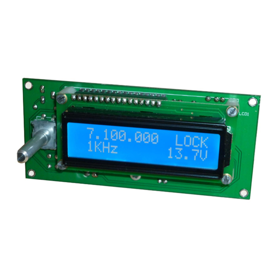
PERATION Power on When the DDS VFO is powered on the version number is displayed briefly. This is followed by the operating display shown in Figure 3. Transmit frequency 7.100.000 1KHz 13.8V Frequency Step Power Supply Voltage Figure 3 Typical LCD operating display... -
Page 14: Options
PTIONS The DDS VFO operates best with a backlit display. The characters are bright and clear and readable in dim environments. The backlight does consume extra current and if minimizing current consumption is a priority then a non-backlit LCD can be used instead. In this case resistor R9 can be left off the board, although leaving it in will not cause any issues.
Need help?
Do you have a question about the DDS VFO and is the answer not in the manual?
Questions and answers