Table of Contents
Advertisement
Quick Links
Programmable Clock Buffer 5P1105/5P1103 Evaluation Board
USER GUIDE
Introduction
The evaluation board is designed to help the customer evaluate the 5P1105/5P1103, the latest additions to the family of
programmable devices in IDT's Timing portfolio. When the board is connected to a PC running IDT Timing Commander™
Software through USB, the device can be configured and programmed to generate frequencies with best-in-class performances.
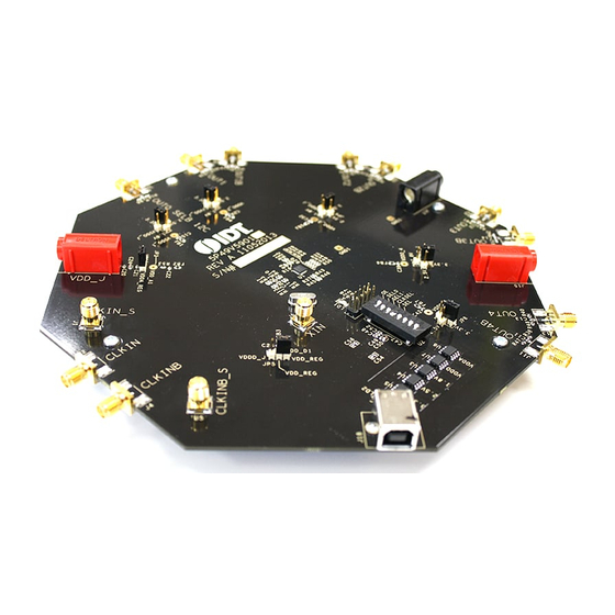
Board Overview
Use the following diagram to identify: power supply jacks, USB connector, input and output frequency SMA connectors.
Figure 1. Board Overview
5P1105
REVISION A 04/13/15
1
©2015 Integrated Device Technology, Inc.
Advertisement
Table of Contents

Related Manuals for Renesas EVK-5P1103ALL


Summary of Contents for Renesas EVK-5P1103ALL
- Page 1 Programmable Clock Buffer 5P1105/5P1103 Evaluation Board USER GUIDE Introduction The evaluation board is designed to help the customer evaluate the 5P1105/5P1103, the latest additions to the family of programmable devices in IDT's Timing portfolio. When the board is connected to a PC running IDT Timing Commander™ Software through USB, the device can be configured and programmed to generate frequencies with best-in-class performances.
-
Page 2: Board Power Supply
PROGRAMMABLE CLOCK BUFFER 5P1105/5P1103 EVALUATION BOARD OUT0 - This is a buffered output of the input reference clock, singled ended. Power supply jack, J16 – Connect to 3.3V, 2.5V or 1.8V for the core voltage of the device. CLKIN_S/CLKINB_S – SMA pair used to monitor the differential input CLKIN/CLKINB. Differential Input clock connector –... - Page 3 PROGRAMMABLE CLOCK BUFFER 5P1105/5P1103 EVALUATION BOARD Figure 2. Jumping to the VDDD_J side will select external bench power supply; Jumping to the VDD_REG side will select power source from on-board regulators powered by USB • Output Clock Voltages Like VDDA and VDDD having two sources, each output voltage VDDO0~4 is also provided with two sources to choose from: bench power supply or powered from USB.
-
Page 4: Connecting The Board
PROGRAMMABLE CLOCK BUFFER 5P1105/5P1103 EVALUATION BOARD Connecting the Board The board is connected to a PC through a USB connector for configuring and programming the device, as shown in Figure 4 below. The USB interface will also provide +5V power supply to the board, from which on-board voltage regulators generate various voltages for the core as well as for each output. -
Page 5: On-Board Crystal
PROGRAMMABLE CLOCK BUFFER 5P1105/5P1103 EVALUATION BOARD On-Board Crystal A 25MHz crystal is installed on the board. It can source a reference frequency to the device when CLKIN/CLKINB is not used. The device can reference from either the crystal or an external clock source. Clock source can be selected within GUI software. Other input reference can be supplied to CLKIN/CLKINB (differential) or XIN (LVCMOS with full swing of 1.2V) connectors. - Page 6 PROGRAMMABLE CLOCK BUFFER 5P1105/5P1103 EVALUATION BOARD Figure 5. Evaluation Board Schematic – Page 1 REVISION A 04/13/15...
- Page 7 PROGRAMMABLE CLOCK BUFFER 5P1105/5P1103 EVALUATION BOARD Figure 6. Evaluation Board Schematic – Page 2 REVISION A 04/13/15...
- Page 8 PROGRAMMABLE CLOCK BUFFER 5P1105/5P1103 EVALUATION BOARD Figure 7. Evaluation Board Schematic – Page 3 REVISION A 04/13/15...
-
Page 9: Signal Termination Options
PROGRAMMABLE CLOCK BUFFER 5P1105/5P1103 EVALUATION BOARD Signal Termination Options Termination options for OUTPUT1 – 4 in the evaluation board are displayed in Figure 8. The termination circuits are designed to optionally terminate the output clocks in LVPECL, LVDS, LVCMOS and HCSL signal types by populating (or not-populating) some resistors. - Page 10 The following evaluation board part numbers are available for order. Table 3. Orderable Part Numbers Part Number Description EVK-5P1103ALL Evaluation board for 5P1103. Output termination configurations are as described in Table 1. EVK-5P1105ALL Evaluation board for 5P1105. Output termination configurations are as described in Table 2.
- Page 11 Corporate Headquarters Sales Tech Support 6024 Silver Creek Valley Road 1-800-345-7015 or email: clocks@idt.com San Jose, CA 95138 USA 408-284-8200 480-763-2056 Fax: 408-284-2775 www.IDT.com DISCLAIMER Integrated Device Technology, Inc. (IDT) and its subsidiaries reserve the right to modify the products and/or specifications described herein at any time and at IDT’s sole discretion. All information in this document, including descriptions of product features and performance, is subject to change without notice.
- Page 12 Koto-ku, Tokyo 135-0061, Japan www.renesas.com/contact/ www.renesas.com Trademarks Renesas and the Renesas logo are trademarks of Renesas Electronics Corporation. All trademarks and registered trademarks are the property of their respective owners.
Need help?
Do you have a question about the EVK-5P1103ALL and is the answer not in the manual?
Questions and answers