Table of Contents
Advertisement
Quick Links
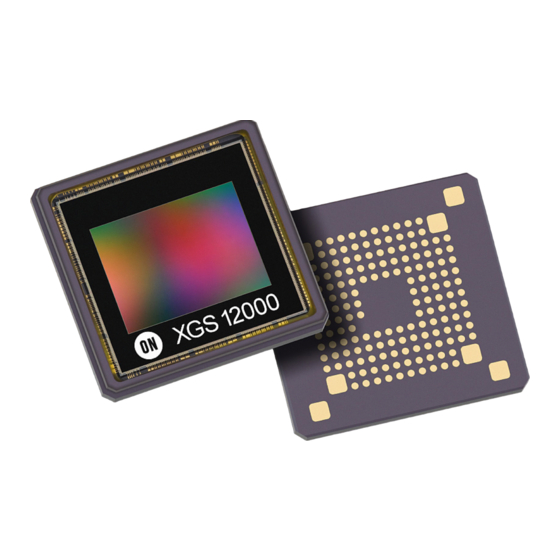
XGS 12000, XGS 9400 and
XGS 8000 Global Shutter
CMOS Image Sensors
XGS Family
Description
The XGS CMOS image sensor family provides high resolution,
high performance global shutter image capture. The family comes in
different resolutions in a single package; 8.8, 9.4 and 12.6 Megapixels
with up to 1−inch optical format. The 21 mm x 20 mm package makes
the XGS family particularly suited for integration in 29 mm x 29 mm
camera formats. The high speed, 12−bit output maximally leverages
interfaces such as USB 3.2, Thunderboltt 2 and 10 GigE.
Image data is read out through a column ADC architecture and then
transferred over a HiSPi interface. On−chip logic, programmable via
the serial interface, generates internal timing for integration and
readout control. Up to three register conÂfigurations can be
programmed and sequentially enabled (frame by frame) using a single
command over the control interface.
Table 1. KEY PERFORMANCE PARAMETERS
Parameter
Optical Format
XGS 12000
XGS 9400
XGS 8000
Active Pixels
XGS 12000
XGS 9400
XGS 8000
Pixel Size
3.2 mm
Color Filter Array
Monochrome, Bayer
Shutter Type
Global Shutter
Input Clock
32.4 MHz
Output Interface
HiSPi (24 Lanes − 777.6 Mbps/lane)
Frame Rate (12−bit)
24 Lanes (−X1)
XGS 12000
XGS 9400
XGS 8000
12 Lanes (−X2)
XGS 9400
XGS 8000
6 Lanes (−X3)
XGS 12000
Read Noise
< 4 e− (1x), 1.9 e
SNR
40 dB
MAX
Dynamic Range
68 dB
Supply Voltages
1.2V, 2.8 V, 3 V (0.4 V, 1.8 V Optional)
Power Consumption
1 W (Full Speed, Full Resolution)
Operating Temp.
−40°C to 85°C (Junction)
Package
163−pin CLGA (Ceramic Land Grid Array)
© Semiconductor Components Industries, LLC, 2018
April, 2020 − Rev. 3
Typical Value
1−inch (16.4 mm Diagonal)
1/1.2−inch (13.9 mm Diagonal)
1/1.1−inch (14.8 mm Diagonal)
4096 (H) x 3072 (V)
3072 (H) x 3072 (V)
4096 (H) x 2160 (V)
90 fps
90 fps
128 fps
56 fps
80 fps
28 fps
−
(4x)
1
www.onsemi.com
Features
•
On−chip 12−bit Column ADCs
•
10−bit Mode with Increased Frame Rate of
100 fps (24−lane) at Full Resolution
•
Companding Mode for 60 fps (12−lane)
and 30 fps (6−lane) at Full Resolution
•
Data Interface: 24−lane HiSPi (Scalable
Low−Voltage Signaling)
•
Configurable Number of HiSPi Lanes:
24, 18, 12 or 6 Lanes
•
2
Two−Wire (I
C) and Four−Wire (SPI)
Serial Interface
•
Triggered Integration and Readout Control
•
Programmable Control for up to 8 Regions
of Interest (ROI)
•
Context Switching
•
These Devices are Pb−Free, Halogen Free/
BFR Free and are RoHS Compliant
Applications
•
Machine Vision
•
Security
•
Intelligent Transportation Systems (ITS)
•
Broadcasting
•
Medical
•
Scientific
Publication Order Number:
XGS12M/D
Advertisement
Table of Contents

Related Manuals for ON Semiconductor XGS 12000

Summary of Contents for ON Semiconductor XGS 12000
- Page 1 XGS 12000, XGS 9400 and XGS 8000 Global Shutter CMOS Image Sensors XGS Family Description www.onsemi.com The XGS CMOS image sensor family provides high resolution, high performance global shutter image capture. The family comes in Features different resolutions in a single package; 8.8, 9.4 and 12.6 Megapixels •...
-
Page 2: Ordering Information
0° CRA NOIX2SE8000B*LTI1 1. See the ON Semiconductor Device Nomenclature document (TND310/D) for a full description of the naming convention used for image sensors. For reference documentation, including information on evaluation kits, please visit our web site at www.onsemi.com. 2. All devices listed in Table 2 are equipped with microlenses. -
Page 3: General Description
XGS Family GENERAL DESCRIPTION all pixels to simultaneously integrate light although the The XGS family from ON Semiconductor covers three subsequent readout is sequential. Note that integration and resolutions: 12.6 Mp, 9.4 Mp and 8.8 Mp and three speed readout can occur in parallel; while reading out one frame, grades (24, 12 or 6 HiSPi lanes). - Page 4 XGS Family • The on−chip logic, programmable through the Two−Wire Sequencer C) or Four−Wire (SPI) Serial Interface, generates all The sequencer generates the sensor timing and controls internal timing for integration control and frame readout. the image core which contains all pixels, driving and Once a row has been read, the data from the columns is readout circuits.
- Page 5 The lines PIXEL ARRAY STRUCTURE accessible through the window configurations are limited to The XGS 12000 active pixel array consists of 4096 the active area region, including interpolation rows. Note columns by 3072 rows of optically active pixels. The active that the windows are configured in logical kernel addresses.
- Page 6 XGS Family Figure 2. XGS 12000 Pixel Array www.onsemi.com...
- Page 7 XGS Family Figure 3. XGS 9400 Pixel Array www.onsemi.com...
- Page 8 XGS Family Figure 4. XGS 8000 Pixel Array www.onsemi.com...
- Page 9 XGS Family Ç Ç Ç Ç Ç Ç Ç Ç Readout Order Frame readout starts by setting the read address to the first Ç Ç Ç Ç Ç Ç Ç Ç row of the configured ROI. Once the row is read, the read Ç...
-
Page 10: Typical Configurations
XGS Family CONFIGURATION AND PINOUT below. The recommended decoupling capacitors are listed in Table 4. TYPICAL CONFIGURATIONS Configuration Example: Two possible configuration examples are depicted in the • _SLVS = 1.2 V (or 0.4 V); V = 1.2 V; V figures below. - Page 11 (1.2 V) (1.2 V) (2.8 V) (3.0 V) 10k W FWSI_EN 32.4 MHz D_CLK_[2,3]_P 100 W EXTCLK D_CLK_[2,3]_N RESET_N DATA_[0:23]_P 100 W DATA_[0:23]_N XGS 12000 CS_N XGS 9400 XGS 8000 DATAOUT DATA TRIG_INT MONITOR_0 TRIG_RD MONITOR_1 MONITOR_2 N.C. RESERVED _PIX _SLVS...
- Page 12 9. I/O signals voltage must be configured to match V _IO voltage to minimize any leakage currents. 10. Digital input RESET_N is active low. 11. ON Semiconductor recommends using a 1.5 kW pull−up resistor to V _IO on both Sclk and Sdata. www.onsemi.com...
- Page 13 XGS Family Table 4. DECOUPLING RECOMMENDATIONS Capacitor Recommended Capacitor Value (mF) Capacitor Recommended Capacitor Value (mF) C1, C5 0.1 + 4.7 0.1 + 2.2 PINOUT Figure 10. XGS CLGA Package Pinout (Top View; Pads Down) www.onsemi.com...
- Page 14 XGS Family PIN LIST Table 5. PIN DESCRIPTIONS (163−PIN LGA PACKAGE) Name LGA Pin Name Type Description A1, A18, C3, C7, C12, C16, F4, F15, Ground Ground G3, G16, J4, J15, K3, K16, M4, M11, M15, N8, N11, P7, P12, T3, T10, T16, V1, V18, D12, F10, G8, G9, G10, G11, P6, P13 _PLL...
- Page 15 XGS Family Table 5. PIN DESCRIPTIONS (163−PIN LGA PACKAGE) Name LGA Pin Name Type Description DATA_4_N HiSPi Differential Data Channel [4], Negative DATA_4_P HiSPi Differential Data Channel [4], Positive DATA_6_N HiSPi Differential Data Channel [6], Negative DATA_6_P HiSPi Differential Data Channel [6], Positive DATA_7_P HiSPi Differential Data Channel [7], Positive...
- Page 16 XGS Family Table 5. PIN DESCRIPTIONS (163−PIN LGA PACKAGE) Name LGA Pin Name Type Description DATA_22_N HiSPi Differential Data Channel [22], Negative DATA_22_P HiSPi Differential Data Channel [22], Positive DATA_23_P HiSPi Differential Data Channel [23], Positive DATA_23_N HiSPi Differential Data Channel [23], Negative DATA_21_P HiSPi Differential Data Channel [21], Positive...
- Page 17 XGS Family SENSOR STATES When in STANDBY mode and upon user intervention the After Power−Up and while the RESET_N pin is driven training patterns or IDLE words can be sent over the video low, the image sensor enters a RESET state until the interface allowing receiver locking.
- Page 18 XGS Family POWER−UP AND POWER−DOWN SEQUENCE 9. The sensor then loads the default register values POWER−UP SEQUENCE from its on−chip memory. As soon as RESET_N is The mandatory Power−Up sequence for the XGS sensor pulled up (released), the sensor starts loading the is shown in Figure 12.
- Page 19 XGS Family Table 7. POWER−UP SEQUENCE Symbol Definition Unit _IO to V _PLL (Note 5) _PLL to V (Note 5) to V (Note 5) to V _PIX/V _PIX_BST/V (Note 5) _PIX/V _PIX_BST/V _RD to V _SLVS (Note 5) EXTCLK Settling Time (Note 4) Hard Reset EXTCLK cycles...
-
Page 20: Power−Down Sequence
XGS Family POWER−DOWN SEQUENCE 3. In STANDBY mode, activate reset by pulling The recommended Power−Down sequence for the down the RESET_N line for at least 30 XGS sensor is shown in Figure 13. The available power EXTCLKs. supplies must have the separation specified below. 4. - Page 21 XGS Family INTEGRATION MODES The whole pixel core is reset simultaneously and after the In a global shutter sensor, light integration takes place on integration time all pixel values are sampled at the same time all pixels in parallel, although subsequent readout is on the storage node inside each pixel.
- Page 22 XGS Family Table 9. INTEGRATION AND FRAME TIMING PARAMETERS Name Description line_time Duration of one line, expressed in logic clock cycles. The minimum line time shall be dictated by the A/D conversion time and readout time (whichever is larger). frame_length Defines the total frame time as frame_length * line_time logic clock periods.
- Page 23 XGS Family MASTER MODE (TRIGGERED) Figure 17. Master Mode (Triggered) In Triggered Master Mode, a rising edge on the edge on the synchronization pin does not have any impact on TRIG_INT pin is used to trigger the start of integration as the readout or integration and subsequent frames are started shown in Figure 17.
- Page 24 XGS Family SLAVE MODE (TRIGGERED) Figure 19. Slave Mode (Triggered) The slave mode depicted in Figure 19 adds more manual As soon as the control pin is asserted, the Sequencer control to the sensor. The integration time registers schedules the SFOT operations. The integration continues (frame_length and integration) are ignored in this mode and until the external pin is deasserted by the user/system.
- Page 25 7. The minimum integration time depends on the configured line time. The values in this table assume the minimum recommended line time is used. 8. Refer to the XGS 12000 Developer Guide for more information on the minimum integration times. www.onsemi.com...
-
Page 26: Readout Modes
= Start of New Line = Readout Figure 21. Frame Triggered Readout Mode XGS 12000 supports two frame triggered readout options, frame_trigger_mode = 1 configurable in the frame_trigger_mode register (refer to In this mode, the trigger acts as an external sequencer Table 11). -
Page 27: Monitor Outputs
XGS Family WAIT_ON_TRIGGER state, in which it is ready to frames per context. The sequencer cycles through the active contexts and generates as many frames as configured per accept a new trigger event. Note that this mode is available for both triggered and context. - Page 28 Extra information about how to implement 10−bit can be found in the XGS 12000, XGS 9400 and XGS 8000 INI file. DATA PEDESTAL The data pedestal is a constant offset that is added to the FRAME RATE pixel values at the end of the datapath.
- Page 29 XGS Family • LANE MULTIPLEXING 4:3 multiplexing: four datapath lanes are multiplexed to The lane multiplexing function can be used to reduce the three HiSPi lanes (total of 18 lanes). number of output data lanes and thus the output data rate. •...
- Page 30 XGS Family The data output on each lane within a single PHY, Figures 31 to 34. The numbers in the squares represent the depending on the multiplexing scheme, is represented in actual column address in the pixel array. 1048 1048 1046 1046 1044...
- Page 31 XGS Family 1, 3, 5 ... 345, 347 DATA _0 (G SYNC BLANK 0, 2, 4 ... 344, 346 DATA _1 (R) SYNC BLANK 349, 351, 353 ... 693, 695 DATA _2 (G SYNC BLANK ‘ 348, 350, 352 ... 692, 694 DATA _3 (R) SYNC BLANK...
-
Page 32: Two−Wire Serial Interface
XGS Family SENSOR CONTROL INTERFACE interface. The four−wire serial interface is recommended for The sensor’s configuration registers are accessible applications requiring fast frequent sensor through either the Two−Wire (I C) or Four−Wire (SPI) (re−)configuration. As shown in Figure 38 below, the type Serial Interface. - Page 33 XGS Family Message Byte place. This transfer takes place as two 8−bit sequences and Message bytes are used for sending register addresses and the slave sends an acknowledge bit after each sequence to register write data to the slave device and for retrieving indicate that the byte has been received.
- Page 34 XGS Family Sequential READ, Start from Random Location has been transferred, the master generates an acknowledge This sequence (Figure 41) starts in the same way as the bit and continues to perform byte READs until “L” bytes single READ from random location (Figure 39). Instead of have been read.
- Page 35 XGS Family Sequential WRITE, Start at Random Location has been transferred, the master generates an acknowledge This sequence (Figure 44) starts in the same way as the bit and continues to perform byte WRITEs until ‘L’ bytes single WRITE to random location (Figure 43). Instead of have been written.
- Page 36 XGS Family FOUR−WIRE SERIAL INTERFACE sends a 15−bit register address followed by a single The sensor’s configuration registers are accessible read/write bit. If the read/write bit is set to 1, the slave reads through a Four−Wire or Serial Peripheral Interface (SPI). the 16−bit data stored at the specified register address and The SPI is a full−duplex, synchronous interface and uses returns it to the master over the S...
-
Page 37: Electrical Specifications
XGS Family ELECTRICAL SPECIFICATIONS _SLVS = 1.2 V; Unless stated otherwise, the following specifications EXTCLK = 32.4 MHz; apply to the following conditions: = 25°C; _PIX = V _PIX_BST = V _RD = 3.0 V; TWO−WIRE SERIAL REGISTER INTERFACE _PLL = 2.8 V; The electrical characteristics of the two−wire serial _IO = 1.8 V;... - Page 38 XGS Family FOUR−WIRE SERIAL INTERFACE and S ) are shown in Figures 50, 51 and 55. The DATAOUT timing parameters are listed in Table 14. The electrical characteristics of the of the Serial Peripheral Interface (SPI) or Four−Wire interface (CS_N, S DATA CS_N 0.2 x V...
- Page 39 XGS Family Table 14. SPI TIMING PARAMETERS Parameter Symbol Unit SPI Read Frequency (PLL disabled / PLL 3.5 / 6.1 enabled) SPI Write Frequency (PLL disabled / PLL 12.5 / 25 enabled) Setup Time (1/fS )*0.1 Hold Time (1/fS )*0.1 Transfer Delay Time (1/fS )*0.5...
-
Page 40: Dc Electrical Characteristics
17. Operating ratings are conditions in which operation of the device is intended to be functional. 18. ON Semiconductor recommends that customers become familiar with, and follow the procedures in JEDEC Standard JESD625 A. Refer to (AN52561/D). Long term exposure toward the maximum storage temperature will accelerate color filter degradation. - Page 41 XGS Family Table 19. OPERATING CURRENT CONSUMPTION (XGS 12000−X1) _PIX = V _PIX_BST = V _RD = 3.0 V; V _PLL = 2.8 V; V _IO = 1.8 V; V = 1.2 V; V _SLVS = 0.4 V / 1.2 V;...
- Page 42 XGS Family Table 22. OPERATING CURRENT CONSUMPTION (XGS 9400−X2) _PIX = V _PIX_BST = V _RD = 3.0 V; V _PLL = 2.8 V; V _IO = 1.8 V; V = 1.2 V; V _SLVS = 0.4 V / 1.2 V; = 25°C) Symbol Parameter...
- Page 43 XGS Family Table 25. STANDBY CURRENT CONSUMPTION _PIX = V _PIX_BST = V _RD = 3.0 V; V _PLL = 2.8 V; V _IO = 1.8 V; V = 1.2 V; V _SLVS = 0.4 V / 1.2 V; = 25°C) Sensor State Condition Unit...
- Page 44 HISPI ELECTRICAL SPECIFICATION this specification when looking at all HiSPi data and HiSPi The XGS sensor from ON Semiconductor supports SLVS clock lanes on the same side of the sensor. The maximum mode only. SLVS is typically meant only for short PHY−to−PHY skew between any odd clock lane and any...
- Page 45 XGS Family DiCLK D_CLK _p DiCLK D_CLK _n DiCLK DiCLK CLKJITTER DCHSKEW DATA _(i)_p DATA _(i)_n CHSKEW 2PHY DATA _(j)_p DATA _(j)_n CMPSKEW Figure 56. Differential Data Output AC Parameters Table 28. DIFFERENTIAL DATA OUTPUT AC SPECIFICATIONS _SLVS = 0.4 V, 1.2 V) Parameter Symbol Unit...
-
Page 46: Electro−Optical Specifications
XGS Family IMAGE SENSOR CHARACTERISTICS ELECTRO−OPTICAL SPECIFICATIONS SPECTRAL RESPONSE An overview of the XGS key electro−optical Quantum efficiency curves are measured using specifications can be found in Table 29. Unless otherwise a monochromator with step size of 5 nm. The curves for noted, all measurements were done using the recommended monochrome and color devices are shown in Figure 57. -
Page 47: Cover Glass
XGS Family COVER GLASS 1000 1100 WAVELENGTH (nm) Figure 58. Cover Glass Transmission Curve Table 30. COVER GLASS SPECIFICATIONS Parameter Specification Material D263 T−ECO Refractive Index (@ 550 nm) 1.5255 Luminous Transmittance (@ D65) 91% (0.55 mm Thickness) Density (@ 40°C) 2.51 g/cm −6 Linear Thermal Coefficient (20°C −... - Page 48 XGS 9400 Radius 5.734 5.11 6.144 5.48 Image Height (%) 6.554 5.84 6.963 6.21 Figure 59. XGS 12000 7.35CRA part Chief Ray Angle vs. Image Height Plot 7.373 6.57 7.782 6.94 8.192 7.30 2160 Pixels / 2 42.2 3.456 3.08 3072 Pixels / 2 4.915...
- Page 49 XGS Family PACKAGING Figure 60. XGS 12000 Shipping Tray − Top View REFERENCES AN52561/D. (n.d.). Image Sensor Handling and Best Practices AND9509/D. (n.d.). High−Speed Serial Pixel (HiSPi) Interface Physical Layer v2.00.00 AND9510/D. (n.d.). High−Speed Serial Pixel (HiSPi) Interface Protocol TND310/D. (n.d.). Device Nomenclature (Naming Convention for Image Sensors) Thunderbolt is a trademark of Intel Corporation or its subsidiaries in the U.S.
-
Page 50: Package Dimensions
ON Semiconductor reserves the right to make changes without further notice to any products herein. ON Semiconductor makes no warranty, representation or guarantee regarding the suitability of its products for any particular purpose, nor does ON Semiconductor assume any liability arising out of the application or use of any product or circuit, and specifically disclaims any and all liability, including without limitation special, consequential or incidental damages. - Page 51 ON Semiconductor reserves the right to make changes without further notice to any products herein. ON Semiconductor makes no warranty, representation or guarantee regarding the suitability of its products for any particular purpose, nor does ON Semiconductor assume any liability arising out of the application or use of any product or circuit, and specifically disclaims any and all liability, including without limitation special, consequential or incidental damages.
- Page 52 FDA Class 3 medical devices or medical devices with a same or similar classification in a foreign jurisdiction or any devices intended for implantation in the human body. Should Buyer purchase or use ON Semiconductor products for any such unintended or unauthorized...
Need help?
Do you have a question about the XGS 12000 and is the answer not in the manual?
Questions and answers