
Related Manuals for GOSUNCN GM500-U1G A


Summary of Contents for GOSUNCN GM500-U1G A
- Page 1 1G_A GM500-U Hardware Development Guide Version: V1.0 Date: 2020-11-20 LTE Module Series Website: www.gosuncnwelink.com E-mail: welink@gosuncn.com...
- Page 2 GM500-U1G_A Hardware Development Guide Revision History Version Date Description 2020-11-20 released version All Rights reserved, No Spreading without GOSUNCN PermissionI...
-
Page 3: About This Document
European Conformity CMOS Complementary Metal Oxide Semiconductor Data Communication Equipment Downlink Data Terminal Equipment Electronic Industries Association Electromagnetic Compatibility Electro-Static discharge Equivalent Series Resistance Frequency Division Duplex GPIO General-purpose I/O Leadless Chip Carrier All Rights reserved, No Spreading without GOSUNCN PermissionII... - Page 4 USIM Universal Subscriber Identity Module Unsolicited result code Logic High level of input voltage Logic Low level of input voltage Logic High level of output voltage Logic Low level of output voltage All Rights reserved, No Spreading without GOSUNCN PermissionIII...
-
Page 5: Safety Information
If not so, GOSUNCN does not take on any liability for customer failure to comply with these precautions. Full attention must be given to driving at all times in order to reduce the risk of an accident. Using a mobile while driving (even with a hands free kit) cause distraction and can lead to an accident. -
Page 6: Table Of Contents
2.10.3. Use ic for level switch ................................43 2.11. Network Status Indication ................................44 2.12. POWER_ON/OFF Status Indicator ON_STATE ..........................45 2.13. ADC Interface ....................................46 2.14. WAKEUP_IN Signal ................................... 47 2.15. WAKEUP_OUT Signal ..................................48 All Rights reserved, No Spreading without GOSUNCN PermissionV... - Page 7 7.3.4. Module Soldering Reflow Curve .............................. 68 7.3.5. Reflow method ..................................69 7.3.6. Maintenance of defects ................................69 7.4. Module’s Baking Requirements ................................. 69 7.4.1. Module’s Baking Environment ..............................69 7.4.2. Baking device and operation procedure ..........................70 All Rights reserved, No Spreading without GOSUNCN PermissionVI...
- Page 8 GM500-U1G_A Hardware Development Guide 7.4.3. Module Baking Conditions ..............................70 All Rights reserved, No Spreading without GOSUNCN PermissionVII...
-
Page 9: Tables
Table 2-24 Pin Definition of USB_BOOT ..................50 Table 2-24 Pin Definition of SD controller Interface ................. 50 Table 2-24 Pin Definition of SGMII Interface ................... 52 Table 3-1 Pin Definition of Antenna ....................54 All Rights reserved, No Spreading without GOSUNCN PermissionVIII... - Page 10 Table 6-2 Testing Environment ....................64 Table 6-3 Testing Instrument & Device..................65 Table 6-4 Reliability Features ....................... 65 Table 7-1 Baking parameters ....................... 66 Table 7-2 LCC module PAD’s steel mesh opening ................66 All Rights reserved, No Spreading without GOSUNCN PermissionIX...
- Page 11 Figure 2–26 Recommended 2-wires UART level switch circuit ............. 44 Figure 2–27 The test point of debug UART .................. 44 Figure 2–28 Reference Circuit of the Network Indicator ............... 45 Figure 2–29 ADC internal structure ....................46 All Rights reserved, No Spreading without GOSUNCN PermissionX...
- Page 12 Figure 7–1 Module Board’s Steel Mesh Diagram ................. 67 Figure 7–2 Material Module Pallet ....................67 Figure 7–3 Tape Reel Dimension ....................68 Figure 7–4 Module Furnace Temperature Curve Reference Diagram .......... 69 All Rights reserved, No Spreading without GOSUNCN PermissionXI...
-
Page 13: Product Overview
1.8V/3V support SIM extraction/hot plug detection Support SIM and USIM UART Interface Support two UART interface: main UART interface and debug UART interface Main UART interface: Eight lines on main UART interface All Rights reserved, No Spreading abroad without GOSUNCN Permission... -
Page 14: Function Diagram
Power management Baseband Memory RF send-receive Peripheral interface --UART interface --USIM card interface --USB interface --SDIO interface --SPI interface --I2C interface --ADC interface --Status interface (LED) All Rights reserved, No Spreading abroad without GOSUNCN Permission... -
Page 15: Evaluation Board
1.4. Evaluation Board In order to help you to develop applications with GM500-U1G_A, GOSUNCN supplies an evaluation board (G2000/GE2015), RS-232 to USB cable, USB data cable, power adapter, antenna and other peripherals to control or test the module. For details, please refer to the related document [GE2015 Dev Board User Guide]. -
Page 16: Application Interface
UART interface Network status indication ADC interface WAKEUP_IN signal WAKEUP_OUT signal GPIO interface 2.2. Pin Assignment The following figure shows the pin assignment of the GM500-U1G_A module. All Rights reserved, No Spreading abroad without GOSUNCN Permission... -
Page 17: Pin Description
GM500-U1G_A Hardware Development Guide Figure 2–1 Pin Assignment 2.3. Pin Description The following table shows the IO Parameters Definition. All Rights reserved, No Spreading abroad without GOSUNCN Permission... -
Page 18: Table 2-1 Io Parameters Definition
Provide 1.8V for Vnorm = 1.8V This pin can only be used for WiFi external circuit Imax = 20mA interface, and can left unconnected when not used. 3,9,11,20,21,31,36, Ground 46,49,52,61,63,78, 80,81,87~102,107, All Rights reserved, No Spreading abroad without GOSUNCN Permission... - Page 19 For 1.8V USIM: Either 1.8V or 3V is supported by the USIM1 card Vmax = 1.9V module automatically Vmin = 1.7V For 3.0V USIM: Vmax = 3.05V Vmin = 2.7V max = 50mA All Rights reserved, No Spreading abroad without GOSUNCN Permission...
- Page 20 = -0.3V 1.8V power domain max = 0.63V min = 1.17V max = 2.1V UART_RTS Request to send min = -0.3V 1.8V power domain max = 0.63V min = 1.17V All Rights reserved, No Spreading abroad without GOSUNCN Permission...
- Page 21 Other firmware, this pin is NC. DO not pull-up external. WLAN_3V3_EN WLAN power enable max = 0.45V Only supported by firmware with WiFi. min = 1.35V Other firmware, this pin is NC All Rights reserved, No Spreading abroad without GOSUNCN Permission...
- Page 22 SD card. Please refer to SD 3.0 max=0.58V controller 2 data bit 2 protocol for details. min=1.27V If do not need SDC, leave this pin not max=2.0V connected. SDC2_DATA1 Secure digital 3.0V: controller 2 data bit 1 All Rights reserved, No Spreading abroad without GOSUNCN Permission...
- Page 23 For 2.85V: max=0.35V min=2.14V SGMII_MDIO_DATA Management data For 1.8V: 1.8V/2.85V power domain input output data max=0.45V If do not need this, leave this pin not min=1.4V connected. max=0.58V min=1.27V All Rights reserved, No Spreading abroad without GOSUNCN Permission...
- Page 24 = 0.45V Pull-up to 1.8V through external 2.2K min = 1.35V resistance. min = -0.3V If do not need I2C, leave this pin not max = 0.63V connected. min = 1.17V All Rights reserved, No Spreading abroad without GOSUNCN Permission...
-
Page 25: Power Supply
= 1.17V VIH max = 2.1V RESERVED 42, 43, 44, 45 RESERVED 2.4. Power Supply 2.4.1. Power Supply Pins The GM500-U1G_A is supplied through the VBAT signal with the following characteristics. All Rights reserved, No Spreading abroad without GOSUNCN Permission... -
Page 26: Decrease Voltage Drop
The over-current capability requirement of DC/DC switching power supply needs to be above 2.5A. When the input and output voltage difference is large, you need to select Buck circuit to improve translate efficiency. The reference power supply circuit design with DC-DC is shown as figure below: All Rights reserved, No Spreading abroad without GOSUNCN Permission... -
Page 27: Turn On Scenarios
The resistors in Figures below are only the recommended value and they need to adjust according to the actual situation. Power-on by dynatron, the circuit ① connect ON/OFF to high level to power-on the module, the circuit ② can connect ON/OFF to low level to power-on the module All Rights reserved, No Spreading abroad without GOSUNCN Permission... -
Page 28: Table 2-5 Definition Of Power_On
The power on scenarios is illustrated as the following figure, the module will power on and working when the POWER_ON pin keep in low level for T1, in this process , please ensure VBAT steady. All Rights reserved, No Spreading abroad without GOSUNCN Permission... -
Page 29: Turn Off Scenarios
The period that the POWER_ON signal for power off operation is second kept on the low PWL The period that the VBAT signal should be kept after power off second operation is down All Rights reserved, No Spreading abroad without GOSUNCN Permission... -
Page 30: Reset Scenarios
When MCU can provide high/low level pulse with 1 second, the reference circuit to reset module is as shown in the following figure below. The resistors in Figures below are only the recommended value and they need to adjust according to the actual situation. All Rights reserved, No Spreading abroad without GOSUNCN Permission... -
Page 31: Figure 2-8Reference Circuit To Reset Module
Module Running Resetting Running Status Figure 2–9Timing of Reset Mode Mode 2: Send command of AT+ZRST, and the RESET process until the AT port can communicate will take 27s at least. All Rights reserved, No Spreading abroad without GOSUNCN Permission... -
Page 32: Usim Card Interface
(send AT command AT+ZSDT=1), and if it is Low, USIM is present; if it is High, USIM is absent. Ground The following figure shows the reference design of the 8-pin USIM card. All Rights reserved, No Spreading abroad without GOSUNCN Permission... -
Page 33: Design Considerations For Usim Card Holder
The pull-up resistor on USIM_DATA line can improve anti-jamming capability when long layout trace and sensitive occasion is applied. 2.8.2. Design Considerations for USIM Card Holder For 8-pin USIM card holder, it is recommended to use Molex 91228. Please visithttp://www.molex.com for more information. All Rights reserved, No Spreading abroad without GOSUNCN Permission... -
Page 34: Table 2-9Pin Description Of Molex Usim Card Holder
USIM card power supply DETECT USIM card Detection Not defined, Connect to Ground For 6-pin USIM card holder, it is recommended to use Amphenol C707 10M006 512 2. Please visit http://www.amphenol.comfor more information. All Rights reserved, No Spreading abroad without GOSUNCN Permission... -
Page 35: Table 2-10Pin Description Of Amphenol Usim Card Holder
Figure 2–13Amphenol C707 10M006 512 2 USIM Card Holder Table 2-10Pin Description of Amphenol USIM Card Holder Pin Name Pin NO. Function Ground Not connected DATA I/O USIM card data USIM card clock All Rights reserved, No Spreading abroad without GOSUNCN Permission... -
Page 36: Usb Interface
Figure 2–14Reference Circuit of USB Application Reference Circuit of USB Communication between module and AP is the one below. The 0Ω in the figure should be placed near pin. All Rights reserved, No Spreading abroad without GOSUNCN Permission... -
Page 37: Figure 2-15Reference Circuit Of Usb Communication Between Module And Ap
Keep the ESD components as closer to the USB connector as possible. All Rights reserved, No Spreading abroad without GOSUNCN Permission... -
Page 38: Uart Interface
8-wires UART connection mode, mainly used for MODEM mode(PPP dialing for example) (DCE) (DTE) Serial Port Serial Port TX D TX D RX D RX D RING RING DS R DS R All Rights reserved, No Spreading abroad without GOSUNCN Permission... -
Page 39: Uart Level Match
We recommend to use audion or IC for UART level match circuit. The pictures below are the recommended level switch circuit for TXD, RXD, CTS, RTS. Each pin recommend two kinds of circuit, and you can select any one if necessarily. All Rights reserved, No Spreading abroad without GOSUNCN Permission... -
Page 40: Figure 2-20Recommended Txd Circuit
GM500-U1G_A Hardware Development Guide Figure 2–20Recommended TXD circuit All Rights reserved, No Spreading abroad without GOSUNCN Permission... -
Page 41: Figure 2-21Recommended Rxd Circuit
GM500-U1G_A Hardware Development Guide Figure 2–21Recommended RXD circuit All Rights reserved, No Spreading abroad without GOSUNCN Permission... -
Page 42: Figure 2-22Recommended Rts Circuit
GM500-U1G_A Hardware Development Guide Figure 2–22Recommended RTS circuit All Rights reserved, No Spreading abroad without GOSUNCN Permission... -
Page 43: Figure 2-23Recommended Cts Circuit
GM500-U1G_A Hardware Development Guide Figure 2–23Recommended CTS circuit All Rights reserved, No Spreading abroad without GOSUNCN Permission... -
Page 44: Use Ic For Level Switch
GM500-U1G_A Hardware Development Guide 2.10.3. Use ic for level switch Figure 2–24Recommended 8-wires UART level switch circuit All Rights reserved, No Spreading abroad without GOSUNCN Permission... -
Page 45: Network Status Indication
The following tables describe pin definition and logic level changes in different network status. Table 2-14Pin Definition of Network Indicator Pin Name Pin NO. Description Comment LED_MODE Indicate the module network registration mode 1.8V power domain All Rights reserved, No Spreading abroad without GOSUNCN Permission... -
Page 46: Power_On/Off Status Indicator On_State
Mode 2:connect this pin to LED to indicate the status of module, the reference circuit you can refer to chapter 2.11. Mode 3:you can connect this pin to test point when in the development stage. All Rights reserved, No Spreading abroad without GOSUNCN Permission... -
Page 47: Adc Interface
1 / 3 ADC channel configuration by default. Figure 2–29 ADC internal structure Table 2-19ADCinterface features(1/3 scaling) Item VIN Min(V) VIN Max(V) channel Minimum input Maximum configuration resistance(MΩ) input current ADC1 VBAT 100 nA ADC2 VBAT 100 nA All Rights reserved, No Spreading abroad without GOSUNCN Permission... -
Page 48: Wakeup_In Signal
When the module needs to be waken up, input a related signal via WAKEUP-IN. The following figure is the signal waveform: High High WAKEUP_IN: Module can Wake up state Module state: Wake up state enter Sleep Figure 2–30 WAKEUP_IN input sequence All Rights reserved, No Spreading abroad without GOSUNCN Permission... -
Page 49: Wakeup_Out Signal
) arrives, the pin output a low-level-voltage pulse lasting for 1s For instance, When a wake-up source arrives, the modulewill output the level shown as the figure below through pin 71. All Rights reserved, No Spreading abroad without GOSUNCN Permission... -
Page 50: Gpio Interface
Module provides 9 GPIO pins. The direction and output voltage level of the GPIO can be set by AT command "AT+ZGPIO". The input voltage level of the GPIO can also be read by AT command "AT+ZGPIO". For more details of these AT commands, please refer to All Rights reserved, No Spreading abroad without GOSUNCN Permission... -
Page 51: Usb_Boot
Secure digital controller 2 data bit 1 3.0 protocol for details. SDC2_DATA0 Secure digital controller 2 data bit 0 If do not need SDC, leave this pin not connected. SDC2_CMD Secure digital controller 2 command All Rights reserved, No Spreading abroad without GOSUNCN Permission... -
Page 52: Figure 2-34 Sd Card Reference Design
50 mm; because the internal wiring length of the module is about 7 mm, the external wiring length needs to be less than 43 mm; All Rights reserved, No Spreading abroad without GOSUNCN Permission... -
Page 53: Sgmii Interface
If do not need SGMII, leave this pin not connected. VREF_L5 SGMIIMDIO signal pull up 1.8V/2.85V power Only used for SGMII MDIO pull up If do not need this, leave this pin not connected. All Rights reserved, No Spreading abroad without GOSUNCN Permission... -
Page 54: Figure 2-34 Sgmii + Ar8033 Typical Connection
Keep SGMII away from other sensitive signals such as analog circuits, RF circuits, audio signals, etc., and away from noise sources such as DCDC and clock signals; SGMII intrapair length match<0.5mm; TX to RX lane spacing and SGMII to all other signals spacing 3x line width. All Rights reserved, No Spreading abroad without GOSUNCN Permission... -
Page 55: Antenna Interface
The reference design of main antenna and Rx-diversity antenna is shown as below. It should reserve a double-L-type matching circuit for better RF performance, and place these components as close as possible to the module. The capacitors are not mounted by default. All Rights reserved, No Spreading abroad without GOSUNCN Permission... -
Page 56: Figure 3-1Reference Circuit Of Antenna Interface
The following picture is the reference of GNSS active antenna, VDD is its power, power supply should be designed by actual requirements. Figure 3–2Reference Circuit of GNSS Antenna NOTE: Keep a proper distance between main and diversity antenna to improve the receiving sensitivity. All Rights reserved, No Spreading abroad without GOSUNCN Permission... -
Page 57: Reference Pcb Layout Of Antenna
PCB layout, guarantee that the metallic shielding shell is fully grounded, so as to leave a smooth discharge channel for ESD. All Rights reserved, No Spreading abroad without GOSUNCN Permission... -
Page 58: Test Methods For Whole-Set Antenna Ota
The main RF instruments are integrated RF test equipment, Spectrum Analyzer, Network Analyzer. The radio equipments, Relay Switch Unit and PC with automatic test software are communicated via GPIB interface. Figure 3–3 The OTA test system of CTIA All Rights reserved, No Spreading abroad without GOSUNCN Permission... -
Page 59: Electrical, Reliability And Radio Characteristics
Table 4-4 Averaged standby DC power consumption [1] Parameter Condition Typical Value Unit OFF state Power down Sleep state Sleep mode ( LTE ) Sleep mode (WCDMA) Sleep mode ( GSM) All Rights reserved, No Spreading abroad without GOSUNCN Permission... -
Page 60: Rf Output Power
LTE FDD Band 4 -100 dBm -97 dBm -94 dBm LTE FDD Band 5 -98 dBm -95 dBm LTE FDD Band 12 -97 dBm -94 dBm LTE FDD Band 13 -97 dBm -94 dBm All Rights reserved, No Spreading abroad without GOSUNCN Permission... -
Page 61: Gnss Technical Parameters
Receiver Type Qualcomm GNSS Gen8C GNSS L1 Frequency 1575.42MHz Update rate 2-4 HZ GNSS (GNSS/GLONASS) data format NMEA data protocol/GOSUNCN defined at commands GNSS (GNSS/GLONASS) Current consumption 65mA GNSS (GNSS/GLONASS) antenna Passive/Active antenna All Rights reserved, No Spreading abroad without GOSUNCN... -
Page 62: Mechanical Dimensions
Hardware Development Guide 5. Mechanical Dimensions This chapter describes the mechanical dimensions of the module. All dimensions are measured in mm. 5.1. Mechanical Dimensions of the Module Figure 5–1GM500-U1G_A Top and Side Dimensions All Rights reserved, No Spreading abroad without GOSUNCN Permission... -
Page 63: Footprint Of Recommendation
GM500-U1G_A Hardware Development Guide Figure 5–2GM500-U1G_A Bottom Dimensions (perspectiveview) Note: The diameter of test point is 1mm. 5.2. Footprint of Recommendation All Rights reserved, No Spreading abroad without GOSUNCN Permission... -
Page 64: Figure 5-3 Recommended Footprint (Perspectiveview)
Keep out the area below the test point (blue area on the above figure) in the host PCB. In order to maintain the module, keep about 3mm between the module and other components in the host PCB. All Rights reserved, No Spreading abroad without GOSUNCN Permission... -
Page 65: Related Test & Test Standard
Table 6-2 lists the extreme working conditions for the Module. Using the Module beyond these conditions may result in permanent damage to the module. Table 6-2 Testing Environment Working Condition Min Temperature Max Temperature Remark All Rights reserved, No Spreading abroad without GOSUNCN Permission... -
Page 66: Reliability Testing Environment
High temperature: +80°C ± 2°C Temperature changing period: less than 30s Test duration: 2 hours Cycle: 10 High-temperature running Normal high temperature: 75 °C GOSUNCN standard Extreme high temperature: 85°C Duration: 24 hours Low-temperature running Normal low temperature: -30°C GOSUNCN standard Extreme low temperature: -40°C... -
Page 67: Smt Process And Baking Guide
Requirements on the thickness of solder paste: control the thickness between 0.18mm and 0.20mm. See the LCC module PAD’s steel mesh opening in the following table: Table 7-2LCC module PAD’s steel mesh opening Steel mesh opening Module PAD GAP (G)=Center Distance (e)-PAD width (X) All Rights reserved, No Spreading abroad without GOSUNCN Permission... -
Page 68: Module Board's Smt Process
1) SMT Tape Reel: The tape reels, which are suitable for SMT, have been made for most GOSUNCN modules. If the module has provided the tape reel itself and meets the SMT requirements, customers can directly use it for module SMT. -
Page 69: Module Soldering Reflow Curve
7.3.4. Module Soldering Reflow Curve Module soldering furnace temperature curve is: Peak value: 245+0/-5℃ ≥217℃: 30〜〜60S 150〜200℃: 60〜〜120S Temperature rise slope: <3℃/S All Rights reserved, No Spreading abroad without GOSUNCN Permission... -
Page 70: Reflow Method
The module must be baked prior to the second reflow. 7.4.1. Module’s Baking Environment The operators must wear dust-free finger cots and anti-static wrist strap under the lead-free and good static-resistant environment. Refer to the following environment requirements: All Rights reserved, No Spreading abroad without GOSUNCN Permission... -
Page 71: Baking Device And Operation Procedure
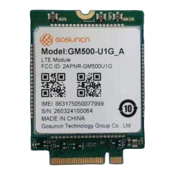
“Contains FCC ID: 2APNR-GM500U1G The FCC ID can be used only when all FCC compliance requirements are met. All Rights reserved, No Spreading abroad without GOSUNCN Permission... - Page 72 If the grantee markets their product as being Part 15 Subpart B compliant (when it also contains unintentional-radiator digital circuity), then the grantee shall provide a notice stating that the final host product still requires Part 15 Subpart B compliance testing with the modular transmitter installed. All Rights reserved, No Spreading abroad without GOSUNCN Permission...
- Page 73 This equipment complies with FCC radiation exposure limits set forth for an uncontrolled environment. This equipment should be installed and operated with minimum distance 20 cm between the radiator & your body. All Rights reserved, No Spreading abroad without GOSUNCN Permission...
Need help?
Do you have a question about the GM500-U1G A and is the answer not in the manual?
Questions and answers