Sign In
Upload
Manuals
Brands
GOSUNCN Manuals
Control Unit
GM500-U1G A
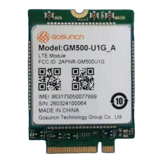
User Manuals: GOSUNCN GM500-U1G A 4G Module
Manuals and User Guides for GOSUNCN GM500-U1G A 4G Module. We have
1
GOSUNCN GM500-U1G A 4G Module manual available for free PDF download: Hardware Development Manual
GOSUNCN GM500-U1G A Hardware Development Manual (73 pages)
Brand:
GOSUNCN
| Category:
Control Unit
| Size: 3 MB
Table of Contents
About this Document
3
Safety Information
5
Table of Contents
6
Tables
9
Product Overview
13
General Description
13
Key Features
13
Table 1-1GM500-U1G_A Supported Band
13
Table 1-2GM500-U1G_A Key Features
13
Function Diagram
14
Evaluation Board
15
Figure 1-1System Connection Structure
15
Application Interface
16
General Description
16
Pin Assignment
16
Pin Description
17
Figure 2-1 Pin Assignment
17
Table 2-1 IO Parameters Definition
18
Table 2-2 Logic Levels Description
18
Table 2-3 Pin Description
18
Power Supply
25
Power Supply Pins
25
Decrease Voltage Drop
26
Reference Circuit of Power Supply
26
Table 2-4Power Supply
26
Figure 2-2 the Input Reference Circuit of VBAT
26
Turn on Scenarios
27
Figure 2-3 Reference Circuit of DC-DC
27
Figure 2-4 Reference Circuit of LDO
27
Table 2-5 Definition of POWER_ON
28
Figure 2-5 Reference Circuit of POWER_ON
28
Turn off Scenarios
29
Table 2-6 Power-On Time
29
Table 2-7Power-Off Time
29
Figure 2-6 Timing of Turning on Mode
29
Reset Scenarios
30
Figure 2-7Timing of Turning off Mode
30
Figure 2-8Reference Circuit to Reset Module
31
Figure 2-9Timing of Reset Mode
31
USIM Card Interface
32
Description of USIM Pins
32
Table 2-8Pin Definition of the USIM Interface
32
Design Considerations for USIM Card Holder
33
Figure 2-10Reference Circuit of the 8 Pin USIM Card
33
Figure 2-11Reference Circuit of the 6 Pin USIM Card
33
Table 2-9Pin Description of Molex USIM Card Holder
34
Figure 2-12Molex 91228 USIM Card Holder
34
Table 2-10Pin Description of Amphenol USIM Card Holder
35
Figure 2-13Amphenol C707 10M006 512 2 USIM Card Holder
35
USB Interface
36
Table 2-11USB Pin Description
36
Figure 2-14Reference Circuit of USB Application
36
Figure 2-15Reference Circuit of USB Communication between Module and AP
37
Figure 2-16 Reference Circuit of USB When USB Is Not the Desired Function
37
UART Interface
38
Uart Connection
38
Table 2-12Pin Definition of the Main UART Interface
38
Table 2-13Pin Definition of the Debug UART Interface
38
Uart Level Match
39
Figure 2-17Schematic of 8-Wire UART Connection
39
Figure 2-18 Schematic of 3-Wire UART Connection
39
Figure 2-19 Schematic of 4-Wire UART Connection
39
Figure 2-20Recommended TXD Circuit
40
Figure 2-21Recommended RXD Circuit
41
Figure 2-22Recommended RTS Circuit
42
Figure 2-23Recommended CTS Circuit
43
Use IC for Level Switch
44
Figure 2-24Recommended 8-Wires UART Level Switch Circuit
44
Network Status Indication
45
Table 2-14Pin Definition of Network Indicator
45
Figure 2-25Recommended 4-Wires UART Level Switch Circuit
45
Figure 2-26Recommended 2-Wires UART Level Switch Circuit
45
Figure 2-27 the Test Point of Debug UART
45
POWER_ON/OFF Status Indicator ON_STATE
46
Table 2-15Working State of the Network Indicator
46
Table 2-16Pin Definition of ON_STATE
46
Figure 2-28Reference Circuit of the Network Indicator
46
ADC Interface
47
Table 2-17 Pin Definition of the ADC
47
Table 2-18 Characteristic of the ADC
47
Table 2-19Adcinterface Features(1/3 Scaling)
47
Figure 2-29 ADC Internal Structure
47
WAKEUP_IN Signal
48
Table 2-20ADC Interface Features(X1 Scaling)
48
Table 2-21 Pin Definition of WAKEUP_IN
48
Figure 2-30 WAKEUP_IN Input Sequence
48
WAKEUP_OUT Signal
49
Table 2-22 Pin Definition of WAKEUP_OUT
49
Figure 2-31 WAKEUP_IN Reference Design
49
GPIO Interface
50
Figure 2-32 the Output Signal of WAKEUP_OUT
50
Figure 2-33 Wakeup_Outreference Design
50
Usb_Boot
51
Sdcardinterface
51
Table 2-23Pin Definition of GPIO
51
Table 2-24 Pin Definition of USB_BOOT
51
Table 2-24 Pin Definition of SD Controller Interface
51
Figure 2-34 Usb_Bootreference Design
51
Figure 2-34 SD Card Reference Design
52
SGMII Interface
53
Table 2-24 Pin Definition of SGMII Interface
53
Figure 2-34 SGMII + AR8033 Typical Connection
54
Antenna Interface
55
Pin Definition
55
Reference Design
55
Table 3-1Pin Definition Ofantenna
55
Figure 3-1Reference Circuit of Antenna Interface
56
Figure 3-2Reference Circuit of GNSS Antenna
56
Reference PCB Layout of Antenna
57
Suggestions for EMC & ESD Design
57
EMC Design Requirements
57
ESD Design Requirements
57
Test Methods for Whole-Set Antenna OTA
58
Figure 3-3 the OTA Test System of CTIA
58
Electrical, Reliability and Radio Characteristics
59
Absolute Maximum Ratings
59
Operating Temperature
59
Electrostatic Discharge
59
GM500-U1G_A Test
59
Current Consumption
59
Table 4-1Absolute Maximum Ratings
59
Table 4-2 Operating Temperature
59
Table 4-3ESD Characteristic
59
Table 4-4 Averaged Standby DC Power Consumption [1]
59
RF Output Power
60
RF Receiving Sensitivity
60
Table 4-5 Averaged Working Current [1]
60
Table 4-6 Averaged Working Current [2]
60
Table 4-7 Conducted RF Output Power
60
Table 4-8 Conducted RF Receiving Sensitivity Typical Value [1]
60
GNSS Technical Parameters
61
Table 4-9 Conducted RF Receiving Sensitivity Typical Value [2]
61
Table 4-10GNSS Technical Parameters
61
Mechanical Dimensions
62
Mechanical Dimensions of the Module
62
Figure 5-1GM500-U1G_A Top and Side Dimensions
62
Footprint of Recommendation
63
Figure 5-2GM500-U1G_A Bottom Dimensions (Perspectiveview)
63
Figure 5-3 Recommended Footprint (Perspectiveview)
64
Related Test & Test Standard
65
Testing Reference
65
Description of Testing Environment
65
Table 6-1 Testing Standard
65
Table 6-2 Testing Environment
65
Reliability Testing Environment
66
Table 6-3 Testing Instrument & Device
66
Table 6-4 Reliability Features
66
SMT Process and Baking Guide
67
Storage Requirements
67
Module Plainness Standard
67
Process Routing Selection
67
Solder Paste Selection
67
Design of Module Pad's Steel Mesh Opening on Main Board
67
Table 7-1Baking Parameters
67
Table 7-2LCC Module Pad's Steel Mesh Opening
67
Module Board's SMT Process
68
Figure 7-1 Module Board's Steel Mesh Diagram
68
Figure 7-2Material Module Pallet
68
Module Soldering Reflow Curve
69
Figure 7-3 Tape Reel Dimension
69
Reflow Method
70
Maintenance of Defects
70
Module's Baking Requirements
70
Module's Baking Environment
70
Figure 7-4Module Furnace Temperature Curve Reference Diagram
70
Baking Device and Operation Procedure
71
Advertisement
Advertisement
Related Products
GOSUNCN GR500
GOSUNCN GW500
GOSUNCN ME3630 mini-PCIE
GOSUNCN ME3630 Series
GOSUNCN ME3630-A
GOSUNCN ME3630-E
GOSUNCN ME3630-J
GOSUNCN ME3630-U
GOSUNCN Categories
Control Unit
GSM/GPRS Modules
Microphone system
Network Router
GPS
More GOSUNCN Manuals
Login
Sign In
OR
Sign in with Facebook
Sign in with Google
Upload manual
Upload from disk
Upload from URL