Sony Cyber-shot DSC-P150 Service Manual
Hide thumbs
Also See for Cyber-shot DSC-P150:
- Specification sheet (2 pages) ,
- Operating instructions manual (128 pages) ,
- Specification (2 pages)
Table of Contents
Advertisement
Quick Links
SERVICE MANUAL
Ver 1.0 2004.08
Revision History
Revision History
How to use
How to use
Acrobat Reader
Acrobat Reader
Link
Link
SPECIFICATIONS
SPECIFICATIONS
SERVICE NOTE
SERVICE NOTE
DISASSEMBLY
DISASSEMBLY
• For ADJUSTMENTS (SECTION 6), refer to SERVICE MANUAL, ADJ (987675551.pdf).
• For INSTRUCTION MANUAL, refer to SERVICE MANUAL, LEVEL 1 (987675541.pdf).
• Reference No. search on printed wiring boards is available.
• Note in Lens Frame Installation
• Exchange Method of Barrier Assy
• HELP: Sheet attachment positions and procedures of processing the flexible boards/harnesses are shown.
On the CH-146 and SY-119 boards
This service manual procides the information that is premised
the circuit board replacement service and not intended repair
inside the CH-146 and SY-119 boards.
Therefore, schematic diagram, printed wiring board and
electrical parts list of the CH-146 and SY-119 boards are not
shown.
The following pages are not shown.
DSC-P150
9-876-755-31
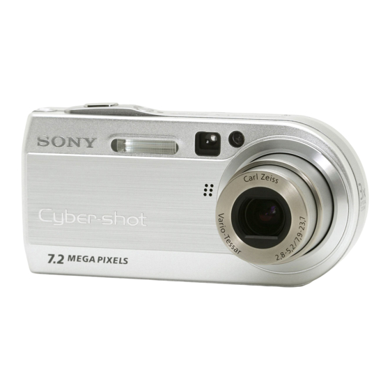
DSC-P150
Photo: Silver
BLOCK DIAGRAMS
BLOCK DIAGRAMS
FRAME SCHEMATIC DIAGRAM
FRAME SCHEMATIC DIAGRAM
SCHEMATIC DIAGRAMS
SCHEMATIC DIAGRAMS
Schematic diagram ............ Pages 4-9 to 4-28
Printed wiring board ........... Pages 4-39 to 4-42
Mounted parts location ....... Pages 4-50 and 4-51
Electrical parts list .............. Pages 5-6 and 5-8 to 5-12
The above-described information is shown in service
manual Level 3.
Sony EMCS Co.
US Model
Canadian Model
AEP Model
UK Model
Hong Kong Model
Australian Model
Brazilian Model
Chinese Model
Korea Model
Tourist Model
Japanese Model
PRINTED WIRING BOARDS
PRINTED WIRING BOARDS
REPAIR PARTS LIST
REPAIR PARTS LIST
DIGITAL STILL CAMERA
Published by DI Technical Support Section
2
LEVEL
E Model
2004H0500-1
©2004.8
Advertisement
Table of Contents

Related Manuals for Sony Cyber-shot DSC-P150


Summary of Contents for Sony Cyber-shot DSC-P150
- Page 1 CH-146 and SY-119 boards are not shown. The above-described information is shown in service The following pages are not shown. manual Level 3. DIGITAL STILL CAMERA 2004H0500-1 DSC-P150 ©2004.8 Sony EMCS Co. 9-876-755-31 Published by DI Technical Support Section...
- Page 2 SPECIFICATIONS x Camera x AC-LS5/LS5B AC Adaptor [LCD screen] [System] LCD panel Input rating 4.6 cm (1.8 type) TFT drive 100 V to 240 V AC, 50/60 Hz, 11 W, Image device 0.16 A to 0.09 A Total number of dots 9.11 mm (1/1.8 type) color CCD 134 000 (560×240) dots Output rating...
- Page 3 CRITIQUES POUR LA SÉCURITÉ DE FONCTIONNEMENT. NE COMPONENTS WITH SONY PARTS WHOSE PART NUMBERS REMPLACER CES COMPOSANTS QUE PAR DES PIÈSES SONY APPEAR AS SHOWN IN THIS MANUAL OR IN SUPPLEMENTS DONT LES NUMÉROS SONT DONNÉS DANS CE MANUEL OU PUBLISHED BY SONY.
-
Page 4: Table Of Contents
TABLE OF CONTENTS Section Title Page SERVICE NOTE 1-1. Note for Repair ································································ 1-1 1-2. Discharging of the ST-105 Flexible Board’s Charging Capacitor (C550) ····························································· 1-1 1-3. Note in Lens Frame Installation ······································ 1-2 1-4. Description on Self-diagnosis Display ···························· 1-2 DISASSEMBLY 2-1. -
Page 5: Service Note
SECTION 1 SERVICE NOTE 1-1. NOTE FOR REPAIR Make sure that the flat cable and flexible board are not cracked of When remove a connector, don’t pull at wire of connector. bent at the terminal. It is possible that a wire is snapped. Do not insert the cable insufficiently nor crookedly. -
Page 6: Note In Lens Frame Installation
1-4. DESCRIPTION ON SELF-DIAGNOSIS DISPLAY Self-diagnosis display • C: ss: ss You can reverse the camera malfunction yourself. (However, contact your Sony dealer or local authorized Sony service facility when you cannot recover from the camera malfunction.) • E: ss: ss Contact your Sony dealer or local authorized Sony service facility. -
Page 7: Disassembly
SECTION 2 HELP HELP DISASSEMBLY 2-1. FLOW CHART The following flow chart shows the disassembly procedure. Note: High-voltage cautions Capacitor R:1 kΩ/1 W (Part code: Discharging the Capacitor 1-215-869-11) Short-circuit between the two points with the short jig about 10 seconds. -
Page 8: Sy-119 Board Service Position
2-2. SY-119 BOARD SERVICE POSITION ST-105 flexible board Lens block Panel block To turn on/off the power, short the circuit between pin 5 and pin 6 (GND) of CN003 on Control switch block (SW) for 1 second. CN003 SY-119 board JK-266 flexible board Control switch block (SW) MS-207 flexible board... -
Page 9: Exchange Method Of Barrier Assy
2-3. EXCHANGE METHOD OF BARRIER ASSY Service parts Part Number Part Name Quantity 3-091-427-01 Ring (A), Ornamental X-3954-476-1 Barrier Assy 3-086-156-31 Tapping screw (P2) Tools used Torque driver Soldering iron Weight about 60g Adhesive (Super X) (Note) Note: Use adhesive (Super X) or an equivalent article. Don’t use what becomes white after drying like a quick-drying glue. -
Page 10: Remove Old Barrier Assy
2-3-2. REMOVE OLD BARRIER ASSY 1 Remove two screws. * Discard the removed screws. 2 Remove the Barrier Assy. * Discard the removed Barrier Assy. * After removing the Barrier Assy, if the “G1 Dust-Proof Ring” was removed, it must be returned to the home position. In returning the ring, adjust the location of a projection to the lens direction. -
Page 11: Adhere The Ornamental Ring A
2-3-4. ADHERE THE ORNAMENTAL RING A Apply an adhesive to four recesses on the top surface of the Barrier Assy. * Do not apply too much adhesive. (Make quantity of adhesives into the quantity in which a groove hides.) Meeting a “notch” of the Ornamental Ring A with a “projection” of the group-1 frame, push the Ornamental Ring A into the group-1 frame. * The projection of the spring for preventing static electricity must be tilted. -
Page 12: Circuit Boards Location
2-4. CIRCUIT BOARDS LOCATION ST-105 flexible (including ST-102) MS-207 flexible CD-517 flexible SY-119 (including CP-101 (CH-146 board) and IC301 (KWF board)) JK-266 flexible CH-146 (included in SY-119) Board Name Function CD-517 flexible CCD IMAGER CH-146 CCD SIGNAL PROCESS (included in SY-119) JK-266 flexible DC IN, MULTI CONNECTOR MS-207 flexible... - Page 13 HELP Sheet attachment positions and procedures of processing the flexible boards/harnesses are shown. SY spacer (MS) CN751 Battery holder assy Shield sheet (SY) DSC-P150 HELP...
-
Page 14: Block Diagrams
3. BLOCK DIAGRAMS Link Link OVERALL BLOCK DIAGRAM (1/2) POWER BLOCK DIAGRAM (1/2) OVERALL BLOCK DIAGRAM (1/2) POWER BLOCK DIAGRAM (1/2) OVERALL BLOCK DIAGRAM (2/2) POWER BLOCK DIAGRAM (2/2) OVERALL BLOCK DIAGRAM (2/2) POWER BLOCK DIAGRAM (2/2) DSC-P150... - Page 15 SECTION 3 3. BLOCK DIAGRAMS 3. BLOCK DIAGRAMS BLOCK DIAGRAMS 3-1. OVERALL BLOCK DIAGRAM (1/2) ( ) : Number in parenthesis ( ) indicates the division number of schematic diagram where the component is located. CD-517 FLEXIBLE BOARD (1/2) SY-119 BOARD (1/2) CONTROL SWITCH CP101 LENS BLOCK (1/2)
-
Page 16: Overall Block Diagram (1/2)
3. BLOCK DIAGRAMS 3. BLOCK DIAGRAMS ( ) : Number in parenthesis ( ) indicates the division number of schematic diagram where the component is located. 3-2. OVERALL BLOCK DIAGRAM (2/2) SY-119 BOARD (2/2) CN101 CN704 (MULTI CONNECTOR) (1/2) JK-266 FLEXIBLE BOARD V OUT V OUT V OUT... -
Page 17: Power Block Diagram (1/2)
3. BLOCK DIAGRAMS 3. BLOCK DIAGRAMS 3-3. POWER BLOCK DIAGRAM (1/2) ( ) : Number in parenthesis ( ) indicates the division number of schematic diagram where the component is located. JK-266 FLEXIBLE BOARD SY-119 BOARD (1/2) CN704 BATT UNREG1 ı... -
Page 18: Power Block Diagram (2/2)
3. BLOCK DIAGRAMS 3. BLOCK DIAGRAMS ( ) : Number in parenthesis ( ) indicates the division number of schematic diagram where the component is located. 3-4. POWER BLOCK DIAGRAM (2/2) SY-119 BOARD (2/2) ST-105 FLEXIBLE ST-102 BOARD BOARD CN706 T501 Q601, 602 L601... -
Page 19: Printed Wiring Boards And Schematic Diagrams
4-2. SCHEMATIC DIAGRAMS 4-2. SCHEMATIC DIAGRAMS 4-3. PRINTED WIRING BOARDS 4-3. PRINTED WIRING BOARDS SECTION 4 PRINTED WIRING BOARDS AND SCHEMATIC DIAGRAMS 4-1. FRAME SCHEMATIC DIAGRAM C550 ST-105 CHARGING CN101 CAPACITOR CAM_-7.5V FLEXIBLE BOARD CN706 STRB_ON ST_5V ST_UNREG ST_UNREG FLASH UNIT ST_UNREG ST_GND ST-102... -
Page 20: Schematic Diagrams
4-2. SCHEMATIC DIAGRAMS Link Link MS-207 FLEXIBLE BOARD MS-207 FLEXIBLE BOARD CD-517 FLEXIBLE BOARD CD-517 FLEXIBLE BOARD (CCD IMAGER) (CCD IMAGER) (MEMORY STICK CONNECTOR) (MEMORY STICK CONNECTOR) ST-105 FLEXIBLE BOARD JK-266 FLEXIBLE BOARD ST-105 FLEXIBLE BOARD JK-266 FLEXIBLE BOARD (CHARGING CAPACITOR) (DC IN, MULTI CONNECTOR) (CHARGING CAPACITOR) (DC IN, MULTI CONNECTOR) - Page 21 4-2. SCHEMATIC DIAGRAMS 4-2. SCHEMATIC DIAGRAMS 4-2. SCHEMATIC DIAGRAMS THIS NOTE IS COMMON FOR SCHEMATIC DIAGRAMS (In addition to this, the necessary note is printed in each block) (For schematic diagrams) 1. Connection • All capacitors are in µF unless otherwise noted. pF : µ Link µF.
- Page 22 4-2. SCHEMATIC DIAGRAMS 4-2. SCHEMATIC DIAGRAMS CD-517 FLEXIBLE BOARD CD-517 FLEXIBLE BOARD For Schematic Diagram • Refer to page 4-37 for printed wiring board. SIGNAL PATH CD-517 FLEXIBLE BOARD Note: CD-517 flexible complete board and IC101 VIDEO are not supplied, but there are included in CCD IMAGER (CCD BLOCK) SIGNAL CCD block assy.
- Page 23 Schematic diagrams of the CH-146 and SY-119 boards are not shown. Pages from 4-9 to 4-28 are not shown. DSC-P150...
- Page 24 CL012 CL011 CL013 CL014 CL027 (To CL054) LND522 CL008 CL017 CL018 CL019 CL020 XE_L R506 C505 0.22u CL036 CL040 CL045 CL050 Q503 CPH3209-SONY-TL-E CL041 CL029 CL046 CL051 CL037 TRANS DRIVE R505 C509 0.047u CL030 CL042 CL047 CL034 CL038 CL043 CL048...
- Page 25 4-2. SCHEMATIC DIAGRAMS 4-2. SCHEMATIC DIAGRAMS MS-207 FLEXIBLE BOARD JK-266 FLEXIBLE BOARD MS-207 FLEXIBLE BOARD JK-266 FLEXIBLE BOARD For Schematic Diagram For Schematic Diagram • Refer to page 4-45 for printed wiring board. • Refer to page 4-46 for printed wiring board. SIGNAL PATH MS-207 FLEXIBLE BOARD JK-266 FLEXIBLE BOARD...
- Page 26 4-2. SCHEMATIC DIAGRAMS 4-2. SCHEMATIC DIAGRAMS CONTROL SWITCH BLOCK (SW) CONTROL SWITCH BLOCK (RL51600) CONTROL SWITCH BLOCK (RL51600) is replaced as block, CONTROL SWITCH BLOCK (SW) is replaced as block, so that PRINTED WIRING BOARD is omitted. so that PRINTED WIRING BOARD is omitted. CN003 REG_GND CL001...
-
Page 27: Cd-517 Flexible Ccd Imager
4-3. PRINTED WIRING BOARDS Link Link CD-517 FLEXIBLE BOARD CD-517 FLEXIBLE BOARD MS-207 FLEXIBLE BOARD MS-207 FLEXIBLE BOARD ST-105 FLEXIBLE BOARD ST-105 FLEXIBLE BOARD JK-266 FLEXIBLE BOARD JK-266 FLEXIBLE BOARD ST-102 BOARD ST-102 BOARD COMMON NOTE FOR PRINTED WIRING BOARDS COMMON NOTE FOR PRINTED WIRING BOARDS MOUNTED PARTS LOCATION CIRCUIT BOARDS LOCATION... -
Page 28: Cd-517 Flexible
4-3. PRINTED WIRING BOARDS 4-3. PRINTED WIRING BOARDS 4-3. PRINTED WIRING BOARDS THIS NOTE IS COMMON FOR PRINTED WIRING BOARDS • : Uses unleaded solder. • Chip parts. Transistor Diode • : Circuit board : Flexible board Pattern from the side which enables seeing. : pattern of the rear side (The other layers’... - Page 29 4-2. SCHEMATIC DIAGRAMS 4-2. SCHEMATIC DIAGRAMS 4-3. PRINTED WIRING BOARDS 4-3. PRINTED WIRING BOARDS MOUNTED PARTS LOCATION MOUNTED PARTS LOCATION CD-517 FLEXIBLE Note for Printed Wiring Board (See page 4-35). : Uses unleaded solder. CD-517 FLEXIBLE BOARD D103 SELF TIMER/ RECORDING D103 D102...
- Page 30 Printed wiring boards of the CH-146 and SY-119 boards are not shown. Pages from 4-39 to 4-42 are not shown. DSC-P150...
- Page 31 4-2. SCHEMATIC DIAGRAMS 4-2. SCHEMATIC DIAGRAMS 4-3. PRINTED WIRING BOARDS 4-3. PRINTED WIRING BOARDS MOUNTED PARTS LOCATION MOUNTED PARTS LOCATION ST-105 FLEXIBLE ST-102 Note for Printed Wiring Board (See page 4-35). Note for Printed Wiring Board (See page 4-35). : Uses unleaded solder. : Uses unleaded solder.
- Page 32 4-2. SCHEMATIC DIAGRAMS 4-2. SCHEMATIC DIAGRAMS 4-3. PRINTED WIRING BOARDS 4-3. PRINTED WIRING BOARDS MS-207 FLEXIBLE JK-266 FLEXIBLE Note for Printed Wiring Board (See page 4-35). Note for Printed Wiring Board (See page 4-35). : Uses unleaded solder. : Uses unleaded solder. MS-207 FLEXIBLE BOARD JK-266 FLEXIBLE BOARD C103...
-
Page 33: Mounted Parts Location
4-3. PRINTED WIRING BOARDS 4-3. PRINTED WIRING BOARDS 4-4. MOUNTED PARTS LOCATION no mark : side A * mark : side B CD-517 FLEXIBLE BOARD C102 C105 C106 C107 D101 D102 D103 D104 IC101 Q101 Q102 Q103 R101 R102 R103 R104 R105 R109... - Page 34 Mounted parts location of the CH-146 and SY-119 boards are not shown. Page 4-50 and 4-51 are not shown. DSC-P150 4-51...
- Page 35 4-3. PRINTED WIRING BOARDS 4-3. PRINTED WIRING BOARDS no mark : side A * mark : side B ST-102 BOARD C505 C507 C509 C511 D501 D502 IC501 Q503 Q506 R504 R506 R510 R511 R512 T501 DSC-P150 ST-102 4-52E...
-
Page 36: Repair Parts List
NOTE NOTE 5. REPAIR PARTS LIST NOTE: Characters A to Z of the electrical parts list indicate location of exploded views in which the desired part is shown. EXPLODED VIEWS EXPLODED VIEWS Link Link CABINET BLOCK SECTION LENS BLOCK SECTION BT HOLDER BLOCK SECTION CABINET BLOCK SECTION LENS BLOCK SECTION... - Page 37 5. REPAIR PARTS LIST 5. REPAIR PARTS LIST SECTION 5 REPAIR PARTS LIST NOTE: • -XX, -X mean standardized parts, so they may have some differences from When indicating parts by reference number, the original one. please include the board name. •...
-
Page 38: Exploded Views
5. REPAIR PARTS LIST 5. REPAIR PARTS LIST 5-1. EXPLODED VIEWS 5-1-1. CABINET BLOCK SECTION ns: not supplied BT holder block section (See page 5-4.) LCD901 D901 Lens block section (See page 5-3.) MIC901 The components identified by Les composants identifiés par une mark 0 or dotted line with marque 0 sont critiques pour la mark 0 are critical for safety. -
Page 39: Lens Block Section
5. REPAIR PARTS LIST 5. REPAIR PARTS LIST 5-1-2. LENS BLOCK SECTION - 5 1 (including CD-517 flexible board and IC101 (CCD IMAGER)) (Note 2) (Note 1) (Note 1) (Note 1) SP901 (Note 1) Be sure to read “2-3. Exchange Method of Barrier Assy”... -
Page 40: Bt Holder Block Section
5. REPAIR PARTS LIST 5. REPAIR PARTS LIST 5-1-3. BT HOLDER BLOCK SECTION ns: not supplied (including BT001) (included in 112) (including ST-102 board) - 1 0 (Note) - 2 0 CN101 BT901 (ns) - 2 6 - 1 1 (Note) CN101 (multi connector) is not supplied, but this is included in JK-266 flexible complete board. -
Page 41: Electrical Parts List
CD-517 5-2. ELECTRICAL PARTS LIST Ref. No. Part No. Description Ref. No. Part No. Description A-1071-923-A CCD BLOCK ASSY CD-517 FLEXIBLE BOARD COMPLETE (Not supplied) ****************************** (CCD block assy is including CD-517 flexible board and IC101 (CCD imager).) < CAPACITOR > C102 1-107-826-11 CERAMIC CHIP 0.1uF... - Page 42 8-719-073-01 DIODE MA111- (K8).S0 0 D502 6-500-962-01 DIODE HAU160C030STP < IC > 0 IC501 6-703-635-01 IC TND721MH5-S-TL-E < TRANSISTOR > 0 Q503 6-550-183-01 TRANSISTOR CPH3209-SONY-TL-E 0 Q506 6-550-891-01 TRANSISTOR GT8G133 (T2LSONY.Q) < RESISTOR > R504 1-218-958-11 RES-CHIP 2.7K 1/16W R506...
- Page 43 Checking supplied accessories. Power cord (1) AC adaptor NP-FR1 battery pack (1) Wrist strap (1) 0 1-769-608-11 (AEP, E) AC-LS5 (1) (not supplied) 2-050-981-01 (SILVER) 0 1-776-985-11 (KR) 0 1-477-730-11 2-050-981-11 (BLUE/BLACK) 0 1-782-476-13 (CH) 0 1-783-374-11 (UK, HK) 0 1-790-107-22 (US, CND) 0 1-790-732-12 (JE, J) 0 1-827-945-11 (AUS) Other accessories...
- Page 44 [Description of main button functions on toolbar of the Adobe Acrobat Reader Ver5.0 (for Windows)] Toolbar Printing a text Reversing the screens displayed once • To reverse the previous screens (operation) one by one, click 1. Click the Print button 2.
- Page 45 Reverse 987675531.pdf Revision History S.M. Rev. Ver. Date History Contents issued 2004.08 Official Release — — DSC-P150...
Need help?
Do you have a question about the Cyber-shot DSC-P150 and is the answer not in the manual?
Questions and answers