Sony DSC-P12 Service Manual
Digital still camera
Hide thumbs
Also See for DSC-P12:
- Operating instructions manual (120 pages) ,
- Service manual (41 pages)
Table of Contents
Advertisement
Quick Links
SERVICE MANUAL
Ver 1.0 2003. 03
Revision History
Revision History
Link
Link
SPECIFICATIONS
SPECIFICATIONS
SERVICE NOTE
SERVICE NOTE
DISASSEMBLY
DISASSEMBLY
• For ADJUSTMENTS (SECTION 6), refer to SERVICE MANUAL, ADJ (987622751.pdf).
• For INSTRUCTION MANUAL, refer to SERVICE MANUAL, LEVEL 1 (987622741.pdf).
• This service manual contains information for Japanese model as well.
• Reference No. search on printed wiring boards is available.
• Note in Lens Frame Installation
• HELP: Sheet attachment positions and procedures of processing the flexible boards/harnesses are shown.
On the JK-243, JK-244 and SY-83 boards
This service manual procides the information that is premised
the circuit board replacement service and not intended repair
inside the JK-243, JK-244 and SY-83 boards.
Therefore, schematic diagram, printed wiring board and
electrical parts list of the JK-243, JK-244 and SY-83 boards are
not shown.
The following pages are not shown.
DSC-P10/P12
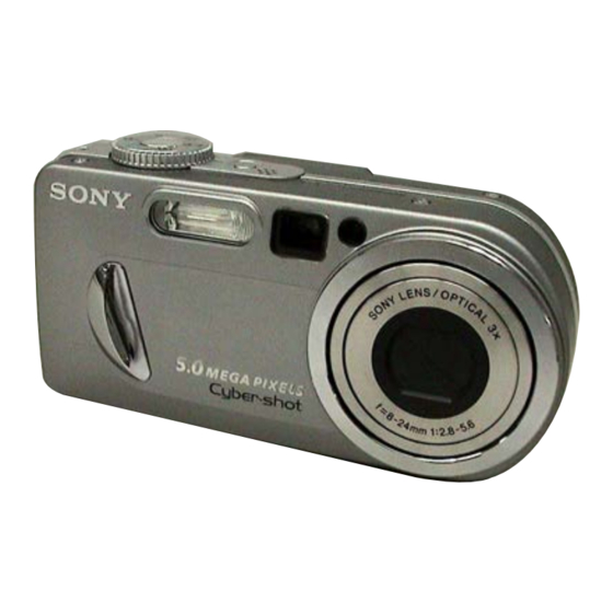
Photo: DSC-P10
BLOCK DIAGRAMS
BLOCK DIAGRAMS
FRAME SCHEMATIC DIAGRAMS
FRAME SCHEMATIC DIAGRAMS
SCHEMATIC DIAGRAMS
SCHEMATIC DIAGRAMS
JK-243, JK-244 boards
Schematic diagram ......................... Pages 4-35 to 4-36
Printed wiring board ........................ Pages 4-51 to 4-52
Electrical parts list ........................... Pages 5-6
SY-83 board
Schematic diagram ......................... Pages 4-9 to 4-28
Printed wiring board ........................ Pages 4-43 to 4-46
Electrical parts list ........................... Pages 5-9 to 5-13
The above-described information is shown in service
manual Level 3.
Canadian Model
AEP Model
Hong Kong Model
Australian Model
Chinese Model
Korea Model
Tourist Model
Japanese Model
PRINTED WIRING BOARDS
PRINTED WIRING BOARDS
REPAIR PARTS LIST
REPAIR PARTS LIST
DIGITAL STILL CAMERA
2
LEVEL
US Model
DSC-P10
UK Model
DSC-P10/P12
E Model
DSC-P10
Advertisement
Table of Contents

Related Manuals for Sony DSC-P12


Summary of Contents for Sony DSC-P12
- Page 1 DSC-P10/P12 SERVICE MANUAL LEVEL US Model Ver 1.0 2003. 03 Canadian Model DSC-P10 Revision History Revision History AEP Model UK Model DSC-P10/P12 E Model Hong Kong Model Australian Model Chinese Model Korea Model Tourist Model Japanese Model Photo: DSC-P10 DSC-P10 Link Link SPECIFICATIONS...
- Page 2 MPEG1 compliant (Monaural) –20°C to +60°C (– 4 °F to +140°F) Accessories Moving images: Dimensions MPEG1 compliant (Monaural) • NP-FC11 battery pack (DSC-P12: 2, DSC-P10: 1) 108×51.5×35.1 mm Recording media • AC-LS5 AC Adaptor (4 3/8×2 1/8×1 7/16 inches) “Memory Stick”...
- Page 3 CRITIQUES POUR LA SÉCURITÉ DE FONCTIONNEMENT. NE COMPONENTS WITH SONY PARTS WHOSE PART NUMBERS REMPLACER CES COMPOSANTS QUE PAR DES PIÈSES SONY APPEAR AS SHOWN IN THIS MANUAL OR IN SUPPLEMENTS DONT LES NUMÉROS SONT DONNÉS DANS CE MANUEL OU PUBLISHED BY SONY.
-
Page 4: Table Of Contents
DSC-P10/P12 TABLE OF CONTENTS Section Title Page SERVICE NOTE 1-1. Note for Repair ································································ 1-1 1-2. Discharging of the ST-81 Flexible Board’s Charging Capacitor (C001) ····························································· 1-1 1-3. Precaution on Replacing the Video Lens or the SY-83 Board ··············································································· 1-2 1-4. -
Page 5: Service Note
DSC-P10/P12 SECTION 1 COVER COVER SERVICE NOTE 1-1. NOTE FOR REPAIR Make sure that the flat cable and flexible board are not cracked of When remove a connector, don’t pull at wire of connector. bent at the terminal. It is possible that a wire is snapped. Do not insert the cable insufficiently nor crookedly. -
Page 6: Precaution On Replacing The Video Lens Or The
DSC-P10/P12 1-3. PRECAUTION ON REPLACING THE 1-4. NOTE IN LENS FRAME VIDEO LENS OR THE SY-83 INSTALLATION BOARD When tightening a screw, have both sides of the lens block assembly so as not for the load to depend. The DSC-P10/P12 uses the position sensor to detect the zoom position. -
Page 7: Description On Self-Diagnosis Display
1-5. DESCRIPTION ON SELF-DIAGNOSIS DISPLAY Self-diagnosis display • C: ss: ss You can reverse the camera malfunction yourself. (However, contact your Sony dealer or local authorized Sony service facility when you cannot recover from the camera malfunction.) • E: ss: ss Contact your Sony dealer or local authorized Sony service facility. -
Page 8: Disassembly
DSC-P10/P12 SECTION 2 COVER COVER HELP HELP DISASSEMBLY The following flow chart shows the disassembly procedure. DISASSEMBLY DISASSEMBLY DISASSEMBLY HELP DISASSEMBLY DISASSEMBLY DISASSEMBLY Discharging the Capacitor DISASSEMBLY HELP DISASSEMBLY DISASSEMBLY HELP DISASSEMBLY DISASSEMBLY DISASSEMBLY DISASSEMBLY HELP SERVICE POSITION DISASSEMBLY DISASSEMBLY HELP... - Page 9 DSC-P10/P12 [SERVICE POSITION] Color monitor JK-244 board SW-386 board LCD module AC power AC IN adaptor SY-83 board - 3 8 Back light unit ST-81 board Memory stick connector Control switch assembly Lens block assembly The procedure for a service position 1 2-2.
-
Page 10: Battery Lid
DSC-P10/P12 Note: Follow the disassembly procedure in the numerical order given. 2-1. BATTERY LID 4 Lid battery 2 Two claws 1 Open the BT lid. 3 BT stopper 2 Screw (1.7 × 3) 2-2. CABINET (REAR) ASSEMBLY 2 Two screws (M1.7) 4 Screw (M1.7) 5 Cabinet (rear) assembly... -
Page 11: Lcd Module
DSC-P10/P12 2-3. LCD MODULE 2 Claw 6 Two bosses 7 Two bosses 4 Flexible board (CN103) 8 LCD module 1 TWO Screws (special) Sheet attachment position 5 Flexible board (CN101) tape (K) 2-4. CABINET FRONT ASSEMBLY 1 Screw (M1.7) 2 Two screws 3 Cabinet front assembly (M1.7) -
Page 12: Control Switch Block
DSC-P10/P12 2-5. CONTROL SWITCH BLOCK Note: High-voltage cautions Discharging the Capacitor Short-circuit between the positive and the negative terminals of charged capacitor 2 Claw with the short jig about 10 seconds. R:1 kΩ/1 W (Part code: 1-215-869-11) Capacitor - 8 1 1 Tape (A) 3 Claw 6 Flexible board... -
Page 13: Cabinet (Lower) Assembly
DSC-P10/P12 2-6. CABINET (LOWER) ASSEMBLY 3 Claw 4 Cabinet (lower) assembly 2 Claw Note: To disengage the claw, pass a flat headed 1 Insert the driver driver under the flexible cable. for removing the claw. It may be a cause of breakage of the flexible Note: High-voltage cautions cable to pass a flat headed driver above the (See page 2-5) -
Page 14: Board
DSC-P10/P12 2-8. ST-81 BOARD Note: High-voltage cautions (See page 2-5) 3 Capacitor insulating sheet 1 Flexible board 4 ST-81 board (CN351) 2 Claw Sheet attachment position Capacitor Capacitor insulating sheet 2-9. SY-83 BOARD 4 Screw (BLACK) 2 Flexible board 3 Flexible board (CN805) 1 Tape (A) (CN801) -
Page 15: Ms-130 Board
DSC-P10/P12 2-10.MS-130 BOARD 2 Claw 1 Screw (BLACK) 3 MS-130 board 2-11.SW-386 BOARD 5 Two bosses 1 Two screws 7 Claw JK-244 board 0 SW-386 board 6 boss 2 Boss 9 Insulating sheet (LI) Sheet attachment position SW-386 board 4 Two screws (BLACK) Note: When you remove the sheet, be careful not to remove... -
Page 16: Cd-434 Board
DSC-P10/P12 2-12.JK-244 BOARD 4 JK-244 board 1 Two claws 3 Claw 2 Boss 2-13.CD-434 BOARD 1 Two screws qs CD-434 board 0 AF holder 4 Two screws 2 Lens frame AF holder 7 Light interception plate qa Remove solders. qs CCD block assy 6 Seal rubber (K) 8 Optical filter block 9 Video lens... -
Page 17: Circuit Boards Location
DSC-P10/P12 2-14.CIRCUIT BOARDS LOCATION SW-386 ST-81 MS-130 CD-434 SY-83 JK-244 (including JK-243) Board Name Function CD-434 CCD IMAGER JK-244 JACK (including JK-243) MS-130 MEMORY STICK CONNECTOR ST-81 FLASH DRIVE SW-386 CONTROL SWITCH, LCD DRIVE, TIMING GENERATOR SY-83 CAMERA MODULE, CAMERA DSP, 256M SDRAM, VIDEO AMP, LENS DRIVE, SH DSP, 16M FLASH, MEMORY, CLOCK GENERATOR, FRONT CONTROL, AUDIO, FLASH CONTROL, DC/DC CONVERTER... - Page 18 DSC-P10/P12 2003.03.28 Update HELP Sheet attachment positions and procedures of processing the flexible boards/harnesses are shown. MAIN BLOCK SECTION Flexible Tape (A) Lens frame board SY insulating sheet Tape (A) Video lens Strobo shade the light sheet SW-386 board Insulating sheet (LI) SY-83 board Secondary lithium battery Insulating sheet (LI)
-
Page 19: Power Block Diagram (1/2)
DSC-P10/P12 COVER COVER 3. BLOCK DIAGRAMS Link Link OVERALL BLOCK DIAGRAM (1/2) POWER BLOCK DIAGRAM (1/2) OVERALL BLOCK DIAGRAM (1/2) POWER BLOCK DIAGRAM (1/2) OVERALL BLOCK DIAGRAM (2/2) POWER BLOCK DIAGRAM (2/2) OVERALL BLOCK DIAGRAM (2/2) POWER BLOCK DIAGRAM (2/2) - Page 20 DSC-P10/P12 SECTION 3 3. BLOCK DIAGRAMS 3. BLOCK DIAGRAMS COVER COVER BLOCK DIAGRAMS 3-1. OVERALL BLOCK DIAGRAM (1/2) ( ) : Number in parenthesis ( ) indicates the division number of schematic diagram where the component is located. LENS BLOCK SY-83 BOARD (1/2) LENS IRIS...
- Page 21 DSC-P10/P12 3. BLOCK DIAGRAMS 3. BLOCK DIAGRAMS COVER COVER ( ) : Number in parenthesis ( ) indicates the division number of schematic diagram where the component is located. 3-2. OVERALL BLOCK DIAGRAM (2/2) SY-83 BOARD (2/2) JK-244 BOARD JK-243 BOARD (1/2) CN805 (1/2)
- Page 22 DSC-P10/P12 3. BLOCK DIAGRAMS 3. BLOCK DIAGRAMS COVER COVER 3-3. POWER BLOCK DIAGRAM (1/2) ( ) : Number in parenthesis ( ) indicates the division number of schematic diagram where the component is located. SY-83 BOARD (1/2) J001 JK-244 BOARD JK-243 BOARD DC IN CN805...
- Page 23 DSC-P10/P12 3. BLOCK DIAGRAMS 3. BLOCK DIAGRAMS COVER COVER ( ) : Number in parenthesis ( ) indicates the division number of schematic diagram where the component is located. 3-4. POWER BLOCK DIAGRAM (2/2) PANEL UNIT SW-386 BOARD IC001 CN802 (1/2) SY-83 BOARD (2/2) Q103...
-
Page 24: Printed Wiring Boards And Schematic Diagrams
DSC-P10/P12 4-2. SCHEMATIC DIAGRAMS 4-2. SCHEMATIC DIAGRAMS 4-3. PRINTED WIRING BOARDS 4-3. PRINTED WIRING BOARDS COVER COVER SECTION 4 PRINTED WIRING BOARDS AND SCHEMATIC DIAGRAMS 4-1. FRAME SCHEMATIC DIAGRAMS 39P CN151 PRE_LAMP CAM_P_5V ST-81 BOARD CN351 XSTRB_PWR_SAVE STB_ON1 STB_FULL ST_UNREG LENZ UNIT ST_UNREG ST_UNREG... - Page 25 DSC-P10/P12 4-2. SCHEMATIC DIAGRAMS 4-2. SCHEMATIC DIAGRAMS COVER COVER 4-2. SCHEMATIC DIAGRAMS THIS NOTE IS COMMON FOR SCHEMATIC DIAGRAMS (In addition to this, the necessary note is printed in each block) (For schematic diagrams) 1. Connection • All capacitors are in µF unless otherwise noted. pF : µ Link µF.
-
Page 26: Schematic Diagrams
DSC-P10/P12 COVER COVER 4-2. SCHEMATIC DIAGRAMS Link Link CD-434 BOARD CD-434 BOARD (CCD IMAGER) ST-81 BOARD (CCD IMAGER) ST-81 BOARD (FLASH DRIVE) (FLASH DRIVE) MS-130 BOARD MS-130 BOARD SW-386 BOARD (1/2) SW-386 BOARD (1/2) (CONTROL SWITCH) (CONTROL SWITCH) (MEMORY STICK CONNECTOR) (MEMORY STICK CONNECTOR) SW-386 BOARD (2/2) SW-386 BOARD (2/2) - Page 27 DSC-P10/P12 4-2. SCHEMATIC DIAGRAMS 4-2. SCHEMATIC DIAGRAMS CD-434 PRINTED WIRING BOARD CD-434 PRINTED WIRING BOARD COVER COVER For Schematic Diagram • Refer to page 4-41 for printed wiring board. CD-434 BOARD Note:Voltage and waveform of mounted on CD-434 board can not be measured because they are (mounted) by the side of the lens.
- Page 28 Schematic diagram of the SY-83 board are not shown. Pages from 4-9 to 4-28 are not shown.
-
Page 29: Sw-386 (1/2) (Control Switch)
DSC-P10/P12 4-2. SCHEMATIC DIAGRAMS 4-2. SCHEMATIC DIAGRAMS SW-386 PRINTED WIRING BOARD SW-386 PRINTED WIRING BOARD COVER COVER For Schematic Diagram • Refer to page 4-47 for printed wiring board. SW-386 BOARD (1/2) CONTROL SWITCH(KEY BLOCK) XX MARK:NO MOUNT NO MARK:REC/PB MODE S004~S008 CONTROL CL001... -
Page 30: Sw-386
DSC-P10/P12 4-2. SCHEMATIC DIAGRAMS 4-2. SCHEMATIC DIAGRAMS SW-386 PRINTED WIRING BOARD SW-386 PRINTED WIRING BOARD COVER COVER For Schematic Diagram • Refer to page 4-47 for printed wiring board. • Refer to page 4-56 for waveforms. SW-386 BOARD (2/2) LCD DRIVE,TIMING GENERATOR(PD BLOCK) XX MARK:NO MOUNT Q103 NO MARK:REC/PB MODE... -
Page 31: Flash Drive
L001 R006 R012 LND021 145619321 1800 FLASH 1/10W TRIGGER UNIT C006 R010 C004 3300p 0.22u C005 1/10W Q002 47000pF CPH3209-SONY-TL-E 250V TRANS DRIVE LND020 Q003 MCH3405-TL-E XE_K(L) R007 100k D002 R008 MA111-(K8).S0 C001 135uF 315V CHARGING CAPACITOR LND001 REG_GND Q004... - Page 32 Schematic diagrams of the JK-243 and JK-244 board are not shown. Pages from 4-35 to 4-36 are not shown.
-
Page 33: Control Switch Block
DSC-P10/P12 4-2. SCHEMATIC DIAGRAMS 4-2. SCHEMATIC DIAGRAMS MS-130 PRINTED WIRING BOARD MS-130 PRINTED WIRING BOARD COVER COVER For Schematic Diagram • Refer to page 4-53 for printed wiring board. MS-130 BOARD CONTROL SWITCH BLOCK MEMORY STICK CONNECTOR(MS BLOCK) CONTROL SWITCH BLOCK is replased as block, so that PRINTED WIRING BOARD is omitted. - Page 34 DSC-P10/P12 4-3. PRINTED WIRING BOARDS 4-3. PRINTED WIRING BOARDS COVER COVER 4-3. PRINTED WIRING BOARDS THIS NOTE IS COMMON FOR PRINTED WIRING BOARDS • : Uses unleaded solder. • Chip parts. • : Circuit board Transistor Diode : Flexible board Pattern from the side which enables seeing.
-
Page 35: Printed Wiring Boards
DSC-P10/P12 COVER COVER 4-3. PRINTED WIRING BOARDS Link Link CD-434 BOARD ST-81 BOARD CD-434 BOARD ST-81 BOARD SW-386 BOARD MS-130 BOARD SW-386 BOARD MS-130 BOARD COMMON NOTE FOR PRINTED WIRING BOARDS WAVEFORMS COMMON NOTE FOR PRINTED WIRING BOARDS WAVEFORMS MOUNTED PARTS LOCATION CIRCUIT BOARDS LOCATION MOUNTED PARTS LOCATION CIRCUIT BOARDS LOCATION... - Page 36 DSC-P10/P12 4-2. SCHEMATIC DIAGRAMS 4-2. SCHEMATIC DIAGRAMS 4-3. PRINTED WIRING BOARDS 4-3. PRINTED WIRING BOARDS MOUNTED PARTS LOCATION MOUNTED PARTS LOCATION COVER COVER CD-434 (CCD IMAGER) Note for Printed Wiring Board (See page 4-39). CD-434 BOARD (SIDE A) CD-434 BOARD (SIDE B) D101 SELF TIMER/ AF ILLUMINATOR...
- Page 37 Printed wiring board of the SY-83 board are not shown. Pages from 4-43 to 4-46 are not shown.
- Page 38 DSC-P10/P12 4-2. SCHEMATIC DIAGRAMS 4-2. SCHEMATIC DIAGRAMS 4-3. PRINTED WIRING BOARDS 4-3. PRINTED WIRING BOARDS MOUNTED PARTS LOCATION MOUNTED PARTS LOCATION COVER COVER SW-386 (LCD DRIVE, TIMING GENERATOR, CONTROL SWITCH) Note for Printed Wiring Board (See page 4-39). SW-386 BOARD D006 S001 S002...
- Page 39 DSC-P10/P12 4-2. SCHEMATIC DIAGRAMS 4-2. SCHEMATIC DIAGRAMS 4-3. PRINTED WIRING BOARDS 4-3. PRINTED WIRING BOARDS MOUNTED PARTS LOCATION MOUNTED PARTS LOCATION COVER COVER ST-81 (FLASH DRIVE) Note for Printed Wiring Board (See page 4-39). ST-81 BOARD (SIDE A) FLASH UNIT ST-81 BOARD (SIDE B) LND019 LND021...
- Page 40 Printed wiring board of the JK-243 and JK-244 board are not shown. Pages from 4-51 to 4-52 are not shown.
- Page 41 DSC-P10/P12 4-2. SCHEMATIC DIAGRAMS 4-2. SCHEMATIC DIAGRAMS 4-3. PRINTED WIRING BOARDS 4-3. PRINTED WIRING BOARDS COVER COVER MS-130 (MEMORY STICK CONNECTOR) Note for Printed Wiring Board (See page 4-39). MS-130 BOARD CN001 1-687-577- MS-130 4-53 4-54...
- Page 42 Waveforms of the SY-83 board are not shown. Page 4-55 is not shown.
-
Page 43: Waveforms
DSC-P10/P12 SW-386 BOARD SW-386 BOARD COVER COVER 4-4. WAVEFORMS SW-386 BOARD 5.0 Vp-p 360 mVp-p IC101 ek REC/PB IC101 wg REC/PB 360 mVp-p 8.2 Vp-p IC101 el REC/PB IC101 wa REC/PB 430 mVp-p 8.2 Vp-p IC101 r; REC/PB IC101 w; REC/PB 3.0 Vp-p 8.2 Vp-p IC101 rs REC/PB... -
Page 44: Mounted Parts Location
DSC-P10/P12 4-3. PRINTED WIRING BOARDS 4-3. PRINTED WIRING BOARDS COVER COVER 4-5. MOUNTED PARTS LOCATION no mark : side A * mark : side B CD-434 BOARD C101 C103 C104 C107 C108 C109 *D101 FB101 IC101 Q101 Q102 R101 R102 R103 R104 R105... - Page 45 Mounted parts location of the SY-83 board are not shown. Page 4-58 is not shown.
- Page 46 DSC-P10/P12 4-3. PRINTED WIRING BOARDS 4-3. PRINTED WIRING BOARDS COVER COVER no mark : side A * mark : side B SW-386 BOARD ST-81 BOARD BT001 * C001 C004 C001 C005 C003 C006 C102 C103 D001 C104 D002 C105 C106 L001 C108 C109...
- Page 47 Mounted parts location of the JK-243 board are not shown. Page 4-60 is not shown.
-
Page 48: Repair Parts List
DSC-P10/P12 COVER COVER NOTE NOTE 5. REPAIR PARTS LIST NOTE: Characters A to C of the electrical parts list indicate location of exploded views in which the desired part is shown. EXPLODED VIEWS EXPLODED VIEWS Link Link CABINET SECTION LENS SECTION BATTERY HOLDER SECTION CABINET SECTION LENS SECTION... - Page 49 DSC-P10/P12 5. REPAIR PARTS LIST 5. REPAIR PARTS LIST COVER COVER SECTION 5 REPAIR PARTS LIST NOTE: • -XX, -X mean standardized parts, so they may have some differences from When indicating parts by reference number, the original one. please include the board name. •...
- Page 50 DSC-P10/P12 5. REPAIR PARTS LIST 5. REPAIR PARTS LIST COVER COVER 5-1. EXPLODED VIEWS 5-1-1. CABINET SECTION ns: not supplied MIC901 Ref. No. Part No. Description Remark Ref. No. Part No. Description Remark X-3953-292-1 CABINET FRONT ASSY (SILVER) 3-081-764-01 FOOT, RUBBER X-3953-441-1 CABINET FRONT ASSY (DEEP BLUE) X-3953-269-2 CABINET (REAR) (A) ASSY (P10: SILVER) 3-080-198-11 SCREW (M1.7), LOCK ACE, P2 (DEEP BLUE)
- Page 51 DSC-P10/P12 5. REPAIR PARTS LIST 5. REPAIR PARTS LIST COVER COVER 5-1-2. LENS SECTION ns: not supplied LCD901 D901 - 4 3 IC101 (Note) (Note) Be sure to read “Precuations for Replacement of CCD Imager” on page 4-8 when changing the CCD imager. The components identified by Les composants identifiés par une mark 0 or dotted line with...
-
Page 52: Battery Holder Section
DSC-P10/P12 5. REPAIR PARTS LIST 5. REPAIR PARTS LIST COVER COVER 5-1-3. BATTERY HOLDER SECTION ns: not supplied - 8 1 - 3 8 - 1 3 BT901 - 8 3 (Note) : BT001 (BATTERY, LITHIUM SECONDARY) Board on the mount position. (See page 4-48.) (Note) Including the parts mounted on JK-243 board. -
Page 53: Electrical Parts List
DSC-P10/P12 CD-434 5-2. ELECTRICAL PARTS LIST Ref. No. Part No. Description Ref. No. Part No. Description A-7078-634-A CD-434 BOARD, COMPLETE *********************** (IC101 is not included in this board) < CAPACITOR > C101 1-107-826-11 CERAMIC CHIP 0.1uF C103 1-162-966-11 CERAMIC CHIP 0.0022uF 10% C104 1-107-826-11 CERAMIC CHIP... - Page 54 (FLASH/CHG (ORANGE)) 0 L001 1-456-193-11 COIL, TRIGGER D101 8-719-017-82 DIODE MA8036 < TRANSISTOR > < IC > 0 Q002 6-550-183-01 TRANSISTOR CPH3209-SONY-TL-E IC001 6-700-712-01 IC NJM2370RD5 (TE2) 0 Q003 8-729-056-01 TRANSISTOR MCH3405-TL-E IC101 8-752-109-23 IC CXA3622R-T4 0 Q004 8-729-053-74 TRANSISTOR CY25AAJ-8-T13 <...
- Page 55 DSC-P10/P12 SW-386 Ref. No. Part No. Description Ref. No. Part No. Description R116 1-208-635-11 RES-CHIP 1/16W R117 1-208-635-11 RES-CHIP 1/16W R120 1-218-973-11 RES-CHIP 1/16W R121 1-218-961-11 RES-CHIP 4.7K 1/16W R122 1-218-981-11 RES-CHIP 220K 1/16W R123 1-218-973-11 RES-CHIP 1/16W R124 1-218-979-11 RES-CHIP 150K 1/16W R125...
- Page 56 DSC-P10/P12 Checking supplied accessories. Power cord (1) AC adaptor NP-FC11 battery pack Wrist strap (1) 0 1-696-819-11 (AUS) AC-LS5 (1) (P10: 1, P12: 2) 3-050-664-11 0 1-769-608-11 (AEP, E) 0 1-477-730-11 (EXCEPT CH) 0 1-776-985-11 (KR) 0 1-477-730-21 (CH) 0 1-782-476-13 (CH) 0 1-783-374-11 (UK, HK) 0 1-790-107-22 (US, CND) 0 1-790-732-11 (JE, J)
- Page 57 DSC-P10/P12 2003C0500-1 Sony EMCS Co. 9-876-227-31 ©2003.3 — 74 — Published by DI Customer Center...
- Page 58 Reverse 987622731.pdf Revision History S.M. Rev. Ver. Date History Contents issued 2003.03 Official Release — —...
Need help?
Do you have a question about the DSC-P12 and is the answer not in the manual?
Questions and answers