Sony DSC-F55 Service Manual
Hide thumbs
Also See for DSC-F55:
- Operating instructions manual (108 pages) ,
- User manual (48 pages) ,
- Specifications (2 pages)
Table of Contents
Advertisement
Quick Links
SERVICE MANUAL
Ver 1.2
With SUPPLEMENT-1 (9-974-166-81)
With SUPPLEMENT-2 (9-974-166-82)
MICROFILM
Downloaded from:
https://www.usersmanualguide.com/
2000.10
DSC-F55/F55E
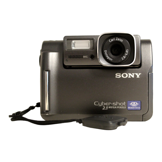
Photo : DSC-F55E
SPECIFICATIONS
US Model
Canadian Model
Tourist Model
AEP Model
UK Model
Australian Model
Hong Kong Model
Chinese Model
DIGITAL STILL CAMERA
DSC-F55
E Model
DSC-F55/F55E
DSC-F55E
Advertisement
Table of Contents

Related Manuals for Sony DSC-F55


Summary of Contents for Sony DSC-F55
- Page 1 DSC-F55/F55E SERVICE MANUAL US Model Canadian Model Tourist Model DSC-F55 Ver 1.2 2000.10 E Model With SUPPLEMENT-1 (9-974-166-81) DSC-F55/F55E With SUPPLEMENT-2 (9-974-166-82) AEP Model UK Model Australian Model Hong Kong Model Chinese Model Photo : DSC-F55E DSC-F55E SPECIFICATIONS DIGITAL STILL CAMERA...
- Page 2 MARK ! ON THE SCHEMATIC DIAGRAMS AND IN THE PARTS CRITIQUES POUR LA SÉCURITÉ DE FONCTIONNEMENT. NE LIST ARE CRITICAL TO SAFE OPERATION. REPLACE THESE REMPLACER CES COMPOSANTS QUE PAR DES PIÈSES SONY COMPONENTS WITH SONY PARTS WHOSE PART NUMBERS DONT LES NUMÉROS SONT DONNÉS DANS CE MANUEL OU APPEAR AS SHOWN IN THIS MANUAL OR IN SUPPLEMENTS DANS LES SUPPÉMENTS PUBLIÉS PAR SONY.
-
Page 3: Table Of Contents
TABLE OF CONTENTS SERVICE NOTE PRINTED WIRING BOARDS AND ····································································· 5 SCHEMATIC DIAGRAMS GENERAL 4-1. Frame Schematic Diagram ·············································· 4-1 Parts identification ····································································· 1-1 4-2. Printed Wiring Boards and Schematic Diagrams ············ 4-4 Preparation ················································································· 1-1 • CD-224 (CCD Imager) 1 Charging the battery pack ···················································... - Page 4 1-3. Video System Adjustments ············································ 5-18 Video Sync Level Adjustment (SY-54 board) ··············· 5-18 Video Burst Level Adjustment (SY-54 board) ··············· 5-18 Video Y Level Check (SY-54 board) ····························· 5-18 1-4. Camera System Adjustments ········································· 5-19 HALL Adjustment ························································· 5-19 Flange Back Adjustment (Using Minipattern Box) ·······...
-
Page 5: Service Note
The electric shock is caused by the charged voltage which is kept without discharging when the main power of the DSC-F55/F55E is simply turned off. Therefore, the remaining voltage must be discharged as described below. - Page 6 [Description on Self-diagnosis Display] Self-diagnosis display • C: ππ: ππ The contents which can be handled by customer, are displayed. Note : The “Self-diagnosis” data is backed up by the coin lithium • E: ππ: ππ battery.The data will be lost and initialized when the coin lithium The contents which can be handled battery is removed.
-
Page 7: General
DSC-F55/F55E SECTION 1 This section is extracted from GENERAL instruction manual. (DSC-F55/F55E) Downloaded from: https://www.usersmanualguide.com/... - Page 8 Downloaded from: https://www.usersmanualguide.com/...
- Page 9 Downloaded from: https://www.usersmanualguide.com/...
- Page 10 Downloaded from: https://www.usersmanualguide.com/...
- Page 11 Downloaded from: https://www.usersmanualguide.com/...
- Page 12 Downloaded from: https://www.usersmanualguide.com/...
- Page 13 Downloaded from: https://www.usersmanualguide.com/...
- Page 14 Downloaded from: https://www.usersmanualguide.com/...
- Page 15 Downloaded from: https://www.usersmanualguide.com/...
- Page 16 1-10 Downloaded from: https://www.usersmanualguide.com/...
- Page 17 1-11 Downloaded from: https://www.usersmanualguide.com/...
- Page 18 1-12E Downloaded from: https://www.usersmanualguide.com/...
-
Page 19: Disassembly
DSC-F55/F55E SECTION 2 DISASSEMBLY The following flow chart shows the disassembly procedure. DSC-F55/F55E 2-1. CABINET (FRONT) ASSEMBLY AND CHECK COVER 2-2. DD-126 BOARD 2-3. LENS CABINET ASSEMBLY 2-5. MM-39, SY-54 BOARDS 2-4. LENS ASSEMBLY, 2-6. CONTROL SWITCH BLOCK (MS) / (HF) MICROPHONE, FLASH UNIT 2-7. -
Page 20: Board
2-2. DD-126 BOARD 8 DD shield case A 6 Remove the solder. 3 Connector 7 DD shield case B CN002 3P (DD-126 board) 1 FP-109 flexible board CN004 (DD-126) 4 Connector CN601 5P (DD-126 board) 5 DD-126 board 2 Two screws (lock ace M1.7) 2-3. -
Page 21: Lens Assembly, Microphone, Flash Unit
2-4. LENS ASSEMBLY, MICROPHONE, FLASH UNIT Note : The built-in charging capacitor inside the FLASH unit is charged to the maximum of 300 V. There is a danger of electric shock due to the high voltage when the capacitor is handed by bare hand. -
Page 22: Boards
2-5. MM-39, SY-54 BOARDS !¢ Screw (lock ace M1.7) !™ FP-109 flexible board !∞ DD flame CN601 (SY-54 board) 9 Harness (SS-72) CN701 (SY-54 board) 4 FP-108 flexible board CN604 (SY-54 board) 5 Flexible board (Control switch block (MS) ) CN603 (SY-54 board) 2 MM-39 board CN351 (SY-54 board) -
Page 23: Lcd Panel Block
2-7. LCD PANEL BLOCK • Open the cabinet in the direction of the arrow A as shown, release the claw of the LCD display panel block, and remove the LCD panel block in the direction of the arrow B . Claw LCD panel block [ SERVICE POSITION 2 (DD-126 BOARD, MM-39 BOARD, SY-54 BOARD, LCD PANEL BLOCK) ]... -
Page 24: Circuit Boards Location
2-8. CIRCUIT BOARDS LOCATION FLASH UNIT CD-224 (CCD IMAGER) MM-39 (MEMORY) INVERTER TRANSFORMER UNIT DD-126 (DC-DC CONVERTER) SY-54 CAMERA, CAMERA DSP, VL-27 LCD DRIVE, TIMING GENERATOR, (BACK UP BATTERY) VIDEO, SH DSP, SERIAL I/O, AUDIO, LENS MOTOR DRIVE, HI CONTROL 2-9. -
Page 25: Block Diagrams
DSC-F55/F55E SECTION 3 BLOCK DIAGRAMS 3-1. OVERALL BLOCK DIAGRAM Downloaded from: https://www.usersmanualguide.com/... -
Page 26: Camera/Memory Stick Block Diagram (1)
3.5Vp-p 0.5V/div 100 nsec IC501 $™ 1.3Vp-p 16.384 MHz 50nsec/div 0.5V/div IC151 @∞ 20nsec/div 1V/div 3.4Vp-p 24.54 MHz (DSC-F55) 24.375 MHz (DSC-F55E) IC102 !£,@º 50 µsec/div 2 V/div 6.5Vp-p 150 µsec IC102 !¢,!ª 50 µsec/div 2 V/div 6.5Vp-p 150 µsec Downloaded from: https://www.usersmanualguide.com/... -
Page 27: Camera/Memory Stick Block Diagram (2)
DSC-F55/F55E 3-3. CAMERA/MEMORY STICK BLOCK DIAGRAM (2) IC351 !¢ (X351,C354) 1.5Vp-p 12.9 MHz 50nsec/div 0.5V/div IC301 !™ A/V OUT 20µsec/div 2.0Vp-p 0.5V/div Q252 E A/V OUT Q251 E, 20µsec/div Q255 E 0.2V/div 0.46Vp-p 0.36Vp-p 20µsec/div 0.1V/div Q253 E LCD 20µsec/div Q254 E LCD 0.1V/div... -
Page 28: Mode Control Block Diagram
DSC-F55/F55E DSC-F55/F55E 3-4. MODE CONTROL BLOCK DIAGRAM IC602 1 3.0Vp-p 32.768 kHz 20µsec/div 1V/div IC603 $º 20MHz OUT 3.0Vp-p 20 MHz 20nsec/div 1V/div 3-11 3-12 Downloaded from: https://www.usersmanualguide.com/... -
Page 29: Lcd Block Diagram
DSC-F55/F55E 3-5. LCD BLOCK DIAGRAM IC802 $¡ LCD 50µsec/div 0.5V/div 1.7Vp-p IC802 @º 4.5Vp-p 20µsec/div 2V/div IC802 @™ 4.5Vp-p 20µsec/div 2V/div IC802 @¢ 4.5Vp-p 20µsec/div 2V/div IC802 8 0.46Vp-p 20µsec/div 0.2V/div IC802 9 LCD 20µsec/div 0.1V/div 0.36Vp-p IC802 0 LCD 0.18Vp-p... -
Page 30: Power Block Diagram
DSC-F55/F55E 3-6. POWER BLOCK DIAGRAM IC001 1 OUT7 0.5µsec/div 0.2V/div 0.8Vp-p 500kHz 3-16 3-17 3-18E Downloaded from: https://www.usersmanualguide.com/... -
Page 31: Printed Wiring Boards And Schematic Diagrams
DSC-F55/F55E SECTION 4 PRINTED WIRING BOARDS AND SCHEMATIC DIAGRAMS 4-1. FRAME SCHEMATIC DIAGRAM FRAME SCHEMATIC DIAGRAM Downloaded from: https://www.usersmanualguide.com/... -
Page 32: Printed Wiring Boards And Schematic Diagrams
DSC-F55/F55E 4-2. PRINTED WIRING BOARDS AND SCHEMATIC DIAGRAMS CD-224 (CCD IMAGER) PRINTED WIRING BOARD — Ref. No. CD-224 Board; 3,000 Series — CD-224 BOARD THIS NOTE IS COMMON FOR WIRING BOARDS AND SCHEMATIC DIAGRAMS (In addition to this, the necessary note is printed in each block) -
Page 33: Camera
• Refer to page 4-37 for printed wiring board. SY-54 BOARD (1/10) 50nsec/div IC152 @§ IC151 #º 1V/div 1.0Vp-p 3.8Vp-p 150 µsec 50µsec/div 12.2727 MHz (DSC-F55) 0.5V/div 12.1875 MHz (DSC-F55E) IC151 #¢ IC152 @º, @£ 20nsec/div 50µsec/div 1V/div 1V/div 3.2Vp-p 3.2Vp-p 150 µsec... -
Page 34: Camera Dsp
DSC-F55/F55E For schematic diagram • Refer to page 4-37 for printed wiring board. SY-54 BOARD (2/10) !¡ Q251 E, 20µsec/div Q255 E 0.2V/div 0.46Vp-p !™ Q252 E A/V OUT 0.36Vp-p 20µsec/div 0.1V/div !£ Q253 E LCD 0.36Vp-p 20µsec/div 0.1V/div !¢... -
Page 35: Lcd Drive
DSC-F55/F55E DSC-F55/F55E For schematic diagram • Refer to page 4-37 for printed wiring board. SY-54 BOARD (3/10) !∞ @™ IC802 $¡ LCD IC802 8 50µsec/div 0.5V/div 0.46Vp-p 1.7Vp-p 20µsec/div 0.2V/div !§ IC802 9 LCD 20µsec/div 0.1V/div 0.36Vp-p !¶ IC802 0 LCD 0.18Vp-p... -
Page 36: Timing Generator
DSC-F55/F55E For schematic diagram • Refer to page 4-37 for printed wiring board. SY-54 BOARD (4/10) @£ IC901 2 4.8Vp-p 20µsec/div 2V/div @¢ IC901 3 4.8Vp-p 20µsec/div 2V/div @∞ IC901 4 4.8Vp-p 20µsec/div 2V/div @§ IC901 @§ 4.1Vp-p 11.722 MHz... -
Page 37: Video
DSC-F55/F55E For schematic diagram • Refer to page 4-37 for printed wiring board. SY-54 BOARD (5/10) @ª IC301 1 A/V OUT 0.46Vp-p 20µsec/div 0.2V/div #º IC301 !ª A/V OUT 0.36Vp-p 20µsec/div 0.1V/div #¡ IC301 !™ A/V OUT 2.0Vp-p 20µsec/div 0.5V/div... -
Page 38: Sh Dsp
DSC-F55/F55E For schematic diagram • Refer to page 4-37 for printed wiring board. SY-54 BOARD (6/10) #™ IC351 !¢ (X351,C354) 1.5Vp-p 12.9 MHz 50nsec/div 0.5V/div SH DSP 4-22 4-23 4-24 SY-54 (6/10) Downloaded from: https://www.usersmanualguide.com/... -
Page 39: Serial I/O
DSC-F55/F55E For schematic diagram • Refer to page 4-37 for printed wiring board. SY-54 BOARD (7/10) #£ IC501 $™ 1.3Vp-p 16.384 MHz 50nsec/div 0.5V/div SERIAL I/O 4-25 4-26 SY-54 (7/10) Downloaded from: https://www.usersmanualguide.com/... -
Page 40: Printed Wiring Board
DSC-F55/F55E For schematic diagram • Refer to page 4-37 for printed wiring board. AUDIO 4-27 4-28 SY-54 (8/10) Downloaded from: https://www.usersmanualguide.com/... - Page 41 DSC-F55/F55E For schematic diagram • Refer to page 4-37 for printed wiring board. LENS MOTOR DRIVE CONTROL SWITCH BLOCK 4-29 4-30 4-31 4-32 SY-54 (9/10) MS / HF Downloaded from: https://www.usersmanualguide.com/...
- Page 42 DSC-F55/F55E DSC-F55/F55E SY-54 BOARD (10/10) #¢ IC603 $º 20MHz OUT 3.0Vp-p 20 MHz 20nsec/div 1V/div #∞ IC602 1 3.0Vp-p 32.768 kHz 20µsec/div 1V/div HI CONTROL 4-34 4-35 4-36 SY-54 (10/10) Downloaded from: https://www.usersmanualguide.com/...
- Page 43 DSC-F55/F55E SY-54 (CAMERA, CAMERA DSP, LCD DRIVE, TIMING GENERATOR, VIDEO, SH DSP, SERIAL I/O, AUDIO, LENS MOTOR DRIVE, HI CONTROL) PRINTED WIRING BOARD SY-54 BOARD — Ref. No. SY-54 Board; 1,000 Series — C151 C284 C-12 C629 B-14 C911 B-13...
- Page 44 DSC-F55/F55E DSC-F55/F55E VL-27 (BACK UP BATTERY) PRINTED WIRING BOARD MM-39 (MEMORY) PRINTED WIRING BOARD — Ref. No. VL-27 Board; 2,000 Series — — Ref. No. MM-39 Board; 1,000 Series — VL-27 BOARD BT691 CN691 A-2 R691 For printed wiring board •...
-
Page 45: Memory
DSC-F55/F55E MEMORY 4-45 4-46 4-47 MM-39 Downloaded from: https://www.usersmanualguide.com/... -
Page 46: Dc-Dc Converter
DSC-F55/F55E DSC-F55/F55E DD-126 (DC-DC CONVERTER) PRINTED WIRING BOARD — Ref. No. DD-126 Board; 2,000 Series — DD-126 BOARD C001 IC001 R020 C002 IC002 R021 C003 R022 C004 L001 R023 C005 L002 R024 C006 L003 R025 C007 L004 R026 C008 L005... - Page 47 DSC-F55/F55E DD-126 BOARD IC001 1 OUT7 0.5µsec/div 0.2V/div 0.8Vp-p 500kHz DC-DC CONVERTER 4-51 4-52 4-53E DD-126 Downloaded from: https://www.usersmanualguide.com/...
-
Page 48: Adjustments
DSC-F55/F55E SECTION 5 ADJUSTMENTS Before starting adjustment EVR Data Re-writing Procedure When Replacing Board The data that is stored in the repair board, is not necessarily correct. Perform either procedure 1 or procedure 2 or procedure 3 when replacing board. -
Page 49: Adjusting Items When Replacing Main Parts And Boards
1-1. Adjusting items when replacing main parts and boards When replacing main parts and boards, adjust the items indicated by r in the following table. Replaced parts Block Mounted parts Board replacement replacement replacement Adjustment Adjustment Section Initialization of B, D, Initialization of D page data E, F page data Initialization of B, E, F page data... -
Page 50: Adjustments
5-1. ADJUSTMENTS 1-1. PREPARATIONS BEFORE ADJUSTMENT 1-1-1. List of Service Tools • Oscilloscope • Color monitor • Vectorscope • Regulated power supply • Digital voltmeter Ref. No. Name Parts Code Usage Auto white balance adjustment/check Filter for color temperature correction (C14) J-6080-058-A White balance adjustment/check ND filter 1.0... -
Page 51: Preparations
1-1-2. Preparations Note 1: For details of how remove the cabinet and boards, refer to “2. Pattern box DISASSEMBLY”. Note 2: When performing only the adjustments, the boards need not be disassembled. 1) Connect the equipment for adjustments according to Fig. 5-1-5. 2) Connect the Adjustment remote commander to SY-54 board CN801 via CPC-9 jig (J-6082-393-C, Note3). - Page 52 VIDEO Terminated at 75 Ω (Yellow) Vector scope Color monitor AUDIO (White) VL-27 BOARD CN691 CN002 CN003 CN604 CN603 CN151 CN602 CN201 CN001 J301 SY-54 DD-126 CN351 A/V OUT BOARD BOARD CN701 CN901 CN605 CN004 CN801 BATTERY terminal MM-39 BOARD 18 pins Extension cable CPC-9 jig...
-
Page 53: Precaution
1-1-4. Precaution 1. Setting the Switch Unless otherwise specified, set the switches as follows and perform adjustments. DEMO MODE (Menu display) ........OFF WHITE BALANCE (Menu display) ......AUTO FLASH LEVEL (Menu display) ......NORMAL EXPOSURE (Menu display) ........... 0EV EFFECT (Menu display) .......... -
Page 54: Initialization Of B, D, E, F Page Data
1-2. INITIALIZATION OF B, D, E, F PAGE DATA 3. D Page Table Note: Fixed data-1 : Initialized data. (Refer to “1. Initializing the D Page 1-2-1. INITIALIZATION OF D PAGE DATA Data”.) 1. Initializing the D Page Data Fixed data-2 : Modified data. (Refer to “2. Modification of D Page Note: If the D page data has been initialized, the following adjustments Data”.) need to be performed again. - Page 55 Remark Remark Initial value Initial value Address Address NTSC PAL NTSC PAL Fixed data-1 Fixed data-1 (Initialized data) (Initialized data) Fixed data-2 Fixed data-1 (Initialized data) Bright adj. (LCD) Battery end adj. Color adj. (LCD) Fixed data-1 White balance adj. (LCD) (Initialized data) Contrast adj.
- Page 56 Remark Remark Initial value Initial value Address Address NTSC PAL NTSC PAL Fixed data-1 Fixed data-1 (Initialized data) (Initialized data) Table. 5-1-2. Fixed data-2 (Modified data, copy the data built in the same model.) Fixed data-1 (Initialized data) Fixed data-2 (Modified data, copy the data built in the same model.) Fixed data-1...
-
Page 57: Modification Of D Page Data
1-2-2. Initializing the B, E, F Page Data 3. F Page table Note: Fixed data-1 : Initialized data. (Refer to “1. Initializing the B, E, F 1. Initializing the B, E, F Page Data Page Data”.) Fixed data-2 : Modified data. (Refer to “2. Modification of B, E, F Note: If the B, E, F Page data has been initialized, “Modification of B, E, Page Data”.) F Page Data”... - Page 58 Remark Remark Initial value Initial value Address Address NTSC PAL NTSC PAL Color reproduction adj. Mechanical shutter adj. Fixed data-1 Fixed data-2 (Initialized data) (Modified data, copy the data built in the same model.) Fixed data-1 Strobe white balance adj. (Initialized data) Fixed data-1 (Initialized data)
- Page 59 Remark Remark Initial value Initial value Address Address NTSC PAL NTSC PAL Fixed data-1 Fixed data-1 (Initialized data) (Initialized data) Table. 5-1-3. 5-12 Downloaded from: https://www.usersmanualguide.com/...
- Page 60 4. E Page Table Address Remark Note: Fixed data-1 : Initialized data. (Refer to “1. Initializing the B, E, F Fixed data-1 Page Data”.) (Initialized data) Fixed data-2 : Modified data. (Refer to “2. Modification of B, E, F Page Data”.) Address Remark Fixed data-1...
- Page 61 Address Remark Address Remark Fixed data-1 Fixed data-1 (Initialized data) (Initialized data) 5-14 Downloaded from: https://www.usersmanualguide.com/...
- Page 62 5. B Page Table Address Remark Note: Fixed data-1 : Initialized data. (Refer to “1. Initializing the B, E, F Fixed data-1 Page Data”.) (Initialized data) Fixed data-2 : Modified data. (Refer to “2. Modification of B, E, F Page Data”.) Remark Initial value Address...
- Page 63 Remark Remark Initial value Initial value Address Address NTSC PAL NTSC PAL Fixed data-1 Fixed data-1 (Initialized data) (Initialized data) CCD defect compensation 5-16 Downloaded from: https://www.usersmanualguide.com/...
- Page 64 Remark Remark Initial value Initial value Address Address NTSC PAL NTSC PAL CCD defect compensation Fixed data-1 (Initialized data) Fixed data-1 (Initialized data) Table. 5-1-5. 5-17 Downloaded from: https://www.usersmanualguide.com/...
-
Page 65: Video System Adjustments
1-3. VIDEO SYSTEM ADJUSTMENTS 2. Video Burst Level Adjustment (SY-54 board) 1. Video Sync Level Adjustment (SY-54 board) Adjust the burst level of the composite video signal output. Adjust the sync level of the composite video signal output. Mode PLAY Mode PLAY Signal... -
Page 66: Camera System Adjustments
1-4. CAMERA SYSTEM ADJUSTMENTS Before perform the camera system adjustments, check that the specified values of “VIDEO SYSTEM ADJUSTMENT” are satisfied. 1. HALL Adjustment For detecting the position of the lens iris, adjust the hall AMP gain and offset. Mode STILL Subject Arbitrary... -
Page 67: Flange Back Adjustment (Using Minipattern Box)
2. Flange Back Adjustment Adjusting method: (Using Minipattern Box) 1) Install the minipattern box so that the distance between it and The inner focus lens flange back adjustment is carried out the front of the lens of the camera is less than 3cm. automatically. -
Page 68: (Using Flange Back Adjustment Chart)
3. Flange Back Adjustment 4. Flange Back Check (Using Flange Back Adjustment Chart) Mode STILL Subject Siemens star The inner focus lens flange back adjustment is carried out (2.0 m from the front of the lens) automatically. In whichever case, the focus will be deviated during (Luminance : approx. -
Page 69: Picture Frame Setting
5. Picture Frame Setting 6. F No. Standard Data Input Compensate the unevenness of the iris meter sensitivity. Mode STILL Mode STILL Subject Color bar chart (Color reproduction adjustment frame) Subject Clear chart (Approx. 33cm from the front of the lens) (Color reproduction adjustment frame) Measurement Point Video output terminal... -
Page 70: Light Level Adjustment
8. Light Level Adjustment 9. Auto White Balance Standard Data Input Adjust the standard LV value. Adjust the white balance standard data at 3200K. Mode STILL Mode STILL Subject Clear chart Subject Clear chart (Color bar standard picture frame) (Color bar standard picture frame) Adjustment Page Adjustment Page Adjustment Address... -
Page 71: Auto White Balance Adjustment
10. Auto White Balance Adjustment Adjust to the proper auto white balance output data. If it is not correct, auto white balance and color reproducibility will be poor. Processing after Completing Adjustments: Mode STILL 1) Select page: E, address: 52, set the data noted down at step 3), Subject Clear chart and press the PAUSE button of the adjustment remote... -
Page 72: Color Reproduction Adjustment
11. Color Reproduction Adjustment 11-2. Color Reproduction Check Adjust the color Separation matrix coefficient so that proper color Mode STILL reproduction is produced. Subject Color bar chart (Color reproduction adjustment frame) 11-1. Color Reproduction Adjustment Measurement Point Video output terminal Mode STILL Measuring Instrument... -
Page 73: White Balance Check
12. White Balance Check 13. Strobe White Balance Adjustment Adjust the white balance when the strobe light flashes. Mode STILL Mode STILL Subject Clear chart (Color reproduction adjustment frame) Subject A plate which reflection rate is 18% (1.0m from the front of the lens) Filter Filter C14 for color temperature correction... -
Page 74: Strobe Light Level And White Balance Check
14. Strobe Light Level and White Balance Check 15. CCD Defect Compensation Check the light level regulation and the white balance when the Mode STILL strobe light flashes. Subject Clear chart Mode STILL (25 cm from the front of the lens) Subject A plate which reflection rate is 18% (Note1) -
Page 75: Ccd Defect Compensation Check
16. CCD Defect Compensation Check Mode STILL Subject Clear chart (25 cm from the front of the lens) (Note) Measurement Point Display data of page: 6, address: 55 Measuring Instrument Adjustment remote commander Specified Value Note 1: Check that there are no dust, no dirt and no reflection on the clear chart. -
Page 76: Lcd System Adjustment
1-5. LCD SYSTEM ADJUSTMENT 1. LCD Initial Data Input Before perform the LCD system adjustments, check that the specified Mode PLAY values of “VIDEO SYSTEM ADJUSTMENT” are satisfied. Signal Arbitrary Note 1: The back light (fluorescent tube) is driven by a high voltage AC Adjustment Page power supply. -
Page 77: Vco Adjustment (Sy-54 Board)
2. VCO Adjustment (SY-54 board) 3. D Range Adjustment (SY-54 board) Set the VCO free-run frequency. If deviated, the LCD screen will Set the D range of the RGB decoder used to drive the LCD to the be blurred. specified value. If deviated, the LCD screen will become blackish or saturated (whitish). -
Page 78: Bright Adjustment (Sy-54 Board)
4. Bright Adjustment (SY-54 board) 5. Contrast Adjustment (SY-54 board) Set the level of the VIDEO signal for driving the LCD to the specified Set the level of the VIDEO signal for driving the LCD to the specified value. If deviated, the screen image will be blackish or saturated value. -
Page 79: Color Adjustment (Sy-54 Board)
6. Color Adjustment (SY-54 board) 7. V-COM Level Adjustment (SY-54 board) Set the color saturation to the standard value. If deviated, the color Set the common electrode drive signal level of LCD to the specified will be to dark or light. value. -
Page 80: V-Com Adjustment (Sy-54 Board)
8. V-COM Adjustment (SY-54 board) 9. White Balance Adjustment (SY-54 board) Set the DC bias of the common electrode drive signal of LCD to the Correct the white balance. specified value. If deviated, the LCD screen color cannot be reproduced. If deviated, the LCD display will move, producing flicker and Mode PLAY... -
Page 81: System Control System Adjustment
1-6. SYSTEM CONTROL SYSTEM ADJUSTMENT 1. Battery End Adjustment (SY-54 board) Check the battery end voltage. Mode STILL Subject Arbitrary Measurement Point Display data of page: 2, address: 51 Measuring Instrument Adjustment remote commander Adjustment Page Adjustment Address 30 to 34, 4A Connection: 1) Connect the regulated power supply and the digital voltmeter to the battery terminal as shown in Fig. -
Page 82: Service Mode
5-2. SERVICE MODE 2-1. ADJUSTMENT REMOTE COMMANDER The adjustment remote commander is used for changing the calculation coefficient in signal processing, EVR data, etc. The adjustment remote commander performs bi-directional communication with the unit using the remote commander signal line (LANC). The resultant data of this bi-directional communication is written in the non-volatile memory. -
Page 83: Data Process
2-2. DATA PROCESS The calculation of the DDS display and the adjustment remote commander display data (hexadecimal notation) are required for obtaining the adjustment data of some adjustment items. In this case, after converting the hexadecimal notation to decimal notation, calculate and convert the result to hexadecimal notation, and use it as the adjustment data. -
Page 84: Service Mode
2-3. SERVICE MODE 2. Bit value discrimination Bit values must be discriminated using the display data of the 1. Setting the Test Mode adjustment remote commander for following items. Use the table below to discriminate if the bit value is “1” or “0”. Page D Address 10 Display on the adjustment remote commander... -
Page 85: Switch Check (1)
3. Switch check (1) Page 2 Address 43 Function When bit value=1 When bit value=0 XPOWER SW (MS block) XCAM/PLAY SW PLAY CAMERA (MS block) SHUTTR SW (MS block) XSHUTTER LOCK SW (MS block) MEMORY STICK IN SW (MS block) XSTILL/MOVIE SW MOVIE STILL... -
Page 86: Repair Parts List
DSC-F55/F55E SECTION 6 REPAIR PARTS LIST 6-1. EXPLODED VIEWS NOTE: • -XX, -X mean standardized parts, so they may • The mechanical parts with no reference number The components identified by mark ! or have some differences from the original one. -
Page 87: Cabinet (Front) Section
6-1-2. CABINET (FRONT) SECTION BT901 not supplied not supplied supplied Ref. No. Part No. Description Remarks Ref. No. Part No. Description Remarks X-3949-590-1 CABINET (FRONT) ASSY 3-050-594-01 SPRING, COMPRESSION 3-054-984-01 TRIPOD 7-624-102-04 STOPRING 1.5, TYPE -E A-7074-055-A VL-27 BOARD, COMPLETE(F55) 3-054-961-01 LID,BATTERY A-7074-059-A VL-27 BOARD, COMPLETE(F55E) 3-355-424-21 SCREW, TAPPING... -
Page 88: Camera Block Section
6-1-3. CAMERA BLOCK SECTION MIC901 IC102 121 113 Be sure to read “Precautions upon replacing CCD imager” on page 4-6 when changing the CCD imager. Ref. No. Part No. Description Remarks Ref. No. Part No. Description Remarks X-3949-592-1 BASE ASSY, LENS 3-054-555-11 RUBBER (K), SEAL 3-054-947-01 RING, FIXED A-7073-995-A CD-224 BOARD, COMPLETE... -
Page 89: Cabinet (Rear) Section
Ver 1.1 1999. 07 6-1-4. CABINET (REAR) SECTION SP901 ND901 156 160 supplied LCD901 not supplied Ref. No. Part No. Description Remarks Ref. No. Part No. Description Remarks 1-673-452-21 FP-110 FLEXIBLE BOARD 1-418-339-11 SWITCH BLOCK, CONTROL (MS) 3-056-030-01 ACE(M1.7),0 PLATE 2 MAIN LOCK X-3949-594-1 CABINET (REAR) ASSY * 153 3-054-949-02 CASE, BL SHIELD... -
Page 90: Electrical Parts List
CD-224 DD-126 6-2. ELECTRICAL PARTS LIST NOTE: • Due to standardization, replacements in the • RESISTORS When indicating parts by reference number, parts list may be different from the parts All resistors are in ohms. please include the board name. specified in the diagrams or the components METAL: metal-film resistor The components identified by mark ! or... - Page 91 DD-126 Ref. No. Part No. Description Remarks Ref. No. Part No. Description Remarks C033 1-115-566-11 CERAMIC CHIP 4.7uF L011 1-414-396-21 INDUCTOR 4.7uH C034 1-115-566-11 CERAMIC CHIP 4.7uF L012 1-414-757-11 INDUCTOR 100uH C035 1-109-994-11 CERAMIC CHIP 2.2uF L013 1-414-757-11 INDUCTOR 100uH C036 1-109-994-11 CERAMIC CHIP 2.2uF...
- Page 92 DD-126 MM-39 Ref. No. Part No. Description Remarks Ref. No. Part No. Description Remarks R012 1-208-719-11 RES,CHIP 0.50% 1/16W R069 1-218-965-11 RES,CHIP 1/16W R013 1-208-715-11 RES,CHIP 0.50% 1/16W R070 1-218-977-11 RES,CHIP 100K 1/16W R014 1-218-970-11 RES,CHIP 1/16W R071 1-218-970-11 RES,CHIP 1/16W R015 1-218-973-11 RES,CHIP...
- Page 93 MM-39 SY-54 Ref. No. Part No. Description Remarks Ref. No. Part No. Description Remarks < IC > < VIBRATOR > IC451 8-759-584-32 IC MB86189PFV-G-BND-ER X451 1-767-621-11 VIBRATOR, CERAMIC (16.93MHz) IC452 8-759-271-88 IC TC7SHU04FU-TE85R * * * * * * * * * * * * * * * * * * * * * * * * * * * * * * * * * * * * * * * * * * * * * * * * * * * * * * * * * * * * IC453 8-759-196-97 IC TC7SH32FU IC454...
- Page 94 SY-54 Ref. No. Part No. Description Remarks Ref. No. Part No. Description Remarks C217 1-164-943-11 CERAMIC CHIP 0.01uF C319 1-164-937-11 CERAMIC CHIP 0.001uF C218 1-164-943-11 CERAMIC CHIP 0.01uF C351 1-125-837-91 CERAMIC CHIP 6.3V C219 1-164-943-11 CERAMIC CHIP 0.01uF C352 1-164-939-11 CERAMIC CHIP 0.0022uF 10% C220 1-117-919-11 TANTAL.
- Page 95 SY-54 Ref. No. Part No. Description Remarks Ref. No. Part No. Description Remarks C641 1-125-777-11 CERAMIC CHIP 0.1uF C814 1-125-837-91 CERAMIC CHIP 6.3V C642 1-125-777-11 CERAMIC CHIP 0.1uF C815 1-104-851-11 TANTAL. CHIP 10uF C643 1-125-777-11 CERAMIC CHIP 0.1uF C816 1-125-777-11 CERAMIC CHIP 0.1uF C644 1-125-777-11 CERAMIC CHIP...
- Page 96 SY-54 Ref. No. Part No. Description Remarks Ref. No. Part No. Description Remarks D903 8-713-102-80 DIODE 1T369-01-T8A IC301 8-759-582-18 IC NJM2538BV(TE2) D904 8-719-976-96 DIODE MA8047-H-TX IC351 8-759-585-34 IC HD6417612RSBP IC353 8-759-484-69 IC MAX3221CAE-TE2 < FERRITE BEAD > IC501 8-752-398-19 IC CXD3147R-T6 IC601 8-759-525-51 IC S-80827HNNP-A9A-T2 FB151...
- Page 97 SY-54 Ref. No. Part No. Description Remarks Ref. No. Part No. Description Remarks Q253 8-729-037-52 TRANSISTOR 2SD2216J-QR(K8).SO R251 1-218-990-11 SHORT Q254 8-729-037-52 TRANSISTOR 2SD2216J-QR(K8).SO R252 1-218-990-11 SHORT Q255 8-729-037-52 TRANSISTOR 2SD2216J-QR(K8).SO R253 1-218-990-11 SHORT Q302 8-729-037-52 TRANSISTOR 2SD2216J-QR(K8).SO R254 1-218-990-11 SHORT Q303 8-729-037-74 TRANSISTOR UN9213J-(K8).SO R257...
- Page 98 SY-54 Ref. No. Part No. Description Remarks Ref. No. Part No. Description Remarks R383 1-218-990-11 SHORT R647 1-218-953-11 RES,CHIP 1/16W R384 1-218-953-11 RES,CHIP 1/16W R648 1-218-989-11 RES,CHIP 1/16W R385 1-218-973-11 RES,CHIP 1/16W R649 1-218-990-11 SHORT R387 1-218-973-11 RES,CHIP 1/16W R652 1-218-990-11 SHORT R390 1-125-777-11 CERAMIC CHIP...
- Page 99 SY-54 VL-27 Ref. No. Part No. Description Remarks Ref. No. Part No. Description Remarks R914 1-218-989-11 RES,CHIP 1/16W MISCELLANEOUS R915 1-218-989-11 RES,CHIP 1/16W ************* R916 1-218-969-11 RES,CHIP 1/16W R918 1-218-975-11 RES,CHIP 1/16W 1-959-605-11 HARNESS (SV-110) R920 1-208-931-11 RES,CHIP 0.50% 1/16W 1-959-606-11 HARNESS (SS-72) 1-673-451-21 FP-109 FLEXIBLE BOARD R921...
- Page 100 Ref. No. Part No. Description Remarks 3-866-543-21 MANUAL, INSTRUCTION(FRENCH)(F55:CND) 3-866-543-31 MANUAL, INSTRUCTION (TRADITIONAL CHINESE)(F55:E) 3-866-543-41 MANUAL, INSTRUCTION(KOREAN)(F55:E) 3-866-544-11 MANUAL, INSTRUCTION(ENGLISH,RUSSIAN) (F55E) 3-866-544-21 MANUAL, INSTRUCTION(GERMAN,FRENCH) (F55E:E,HK,AEP,CN) 3-866-544-31 MANUAL, INSTRUCTION(ITALIAN,DUTCH) (F55E:AEP) 3-866-544-41 MANUAL, INSTRUCTION (SPANISH,PORTUGUESE)(F55E:AEP,E,HK) 3-866-544-61 MANUAL, INSTRUCTION(ARABIC,PERSIAN) (F55E:E,CN) 3-866-544-71 MANUAL, INSTRUCTION (SIMPLIFIED CHINESE)(F55E:CN) A-7033-586-A CORD ASSY(A), POWER(F55:JE) A-7033-588-A CORD ASSY(C), POWER(F55E:AUS)
- Page 101 〈PARTS REFERENCE SHEET〉 You can find the parts position of location of mount locations applying to SY-54 board of a set. SY-54 SIDE A DSC-F55/F55E IC351 IC251 IC501 IC252 — 152 — Downloaded from: https://www.usersmanualguide.com/...
- Page 102 FOR CAMERA COLOR REPRODUCTION ADJUSTMENT 〈 〉 For NTSC model DSC-F55 Take a copy of CAMERA COLOR REPRODUCTION FRAME and Parts referencesheets with a clear sheet for use. For PAL model DSC-F55E — 153 — Downloaded from: https://www.usersmanualguide.com/...
- Page 103 DSC-F55/F55E Sony Corporation 99D1634-1 Personal VIDEO Products Company 9-974-166-11 Printed in Japan ©1999.4 — 154 — Published by Safety & Service Engineering Dept. Downloaded from: https://www.usersmanualguide.com/...
- Page 104 • Parts information correction • Korea model is added to the DSC-F55. The Korea model is same as DSC-F55: E model except accessories. For the accessories, refer to the page 16. • Suffix numbers of the boards are changed as shown below.
- Page 105 : Added portion. Page Changed contents CD-224 PRINTED WIRING BOARD (suffix No. -12) CD-224 BOARD C101 C102 C103 C104 C105 C106 C107 C108 C109 C110 C111 C112 C113 C114 C115 C116 C117 CN101 C-1 CN102 C-3 IC101 IC102 L101 L102 Q101 Q102 R101...
- Page 106 MM-39 PRINTED WIRING BOARD (suffix No. -22 and -23) DD-126 PRINTED WIRING BOARD (suffix No. -23) [ ]: Page No. shown in [ ] indicates the page to refer on the original Service Manual DSC-F55/F55E. There are few cases that the part printed on this diagram isn’t mounted in this model.
- Page 107 DSC-F55/F55E [ Page 4-51 ] DD-126 BOARD SCHEMATIC DIAGRAM [ ]: Page No. shown in [ ] indicates the page to refer on the original Service Manual DSC-F55/F55E. — 6 — — 7 — — 8 — Downloaded from: https://www.usersmanualguide.com/...
- Page 108 : Changed portion. Page Changed contents 1-2-1. INITIALIZATION OF D PAGE DATA 3. D Page Table Remark Initial value Address NTSC PAL Fixed data-2 (Modified data, copy the data built in the same model.) Fixed data-1 (Initialized data) 1-2-2. Initializing the B, E, F Page Data 3.
- Page 109 : Changed portion. Page Changed contents 3. F Page table Remark Initial value Address NTSC PAL Fixed data-1 (Initialized data) Fixed data-2 Fixed data-1 (Initialized data) Fixed data-2 Fixed data-1 (Initialized data) Fixed data-2 (Modified data, copy the data built in the same model.) Fixed data-1 Fixed data-2...
- Page 110 : Changed portion. Page Changed contents 4. E Page Table Address Remark Fixed data-2 Fixed data-1 (Initialized data) Fixed data-2 (Modified data, copy the data built in the same model.) 5-13 Fixed data-1 (Initialized data) Fixed data-2 Fixed data-1 (Initialized data) Fixed data-2 Fixed data-1 (Initialized data)
- Page 111 : Changed portion. Page Changed contents 4. E Page Table Address Remark Fixed data-2 (Modified data, copy the data built in the same model.) Fixed data-1 (Initialized data) Fixed data-2 Fixed data-1 Fixed data-2 (Modified data, copy the data built in the same model.) Fixed data-1 (Initialized data)
- Page 112 : Changed portion. Page Changed contents 4. E Page Table Address Remark Fixed data-2 Fixed data-1 (Initialized data) Fixed data-2 (Modified data, copy the data built in the same model.) Fixed data-1 (Initialized data) Fixed data-2 Fixed data-1 Fixed data-2 Fixed data-1 Fixed data-2 (Modified data, copy the data built in...
- Page 113 : Changed portion. Page Changed contents 5. B Page Table Remark Initial value Address NTSC PAL Fixed data-1 (Initialized data) 5-16 Fixed data-2 (Modified data, copy the data built in the same model.) Fixed data-1 (Initialized data) SECTION 6. REPAIR PARTS LIST : Changed portion.
- Page 114 : Added portion. : Changed portion. : Deleted portion. Page Ref. No. Part No. Description Remarks Ref. No. Part No. Description Remarks 6-2. ELECTRICAL PARTS LIST CD-224 BOARD, COMPLETE ********************** C117 1-164-943-11 CERAMIC CHIP 0.01uF 10% DD-126 BOARD, COMPLETE ********************** D062 8-719-056-61 DIODE MAZS082008SO R026...
- Page 115 DSC-F55/F55E [Addition of Korea model] The following table shows accessories of the DSC-F55: Korea model. Page DSC-F55 : Korea Model Ref. No. Part No. Description Remarks ACCESSORIES ************ 1-475-851-33 ADAPTOR, AC 1-772-118-11 COMPACT DISK 1-782-984-21 CABLE, DIGITAL STILL CAMERA(DOS/V)(1.5m) 1-783-738-31 CORD, CONNECTION (AV)(1.5m) 1-783-739-22 CORD, CONNECTION (DK-115)(1.6m)
- Page 116 (PV00-014) Subject: Change of part code. The assembly parts and the constituent parts are changed as follows. Refer to the DSC-F55/F55E Service Manual (9-974-166-11) and SUPPLEMENT-1 (9-974-166-81) together with the SUPPLEMENT-2 when repairing the units. SECTION 6. REPAIR PARTS LIST 6-1.
- Page 117 DSC-F55/F55E : Changed portion. Page Ref. No. Part No. Description Remarks Ref. No. Part No. Description Remarks X-3949-592-1 BASE ASSY, LENS X-3949-592-5 BASE ASSY, LENS X-3949-593-1 CABINET (REAR) ASSY, LENS(F55) X-3949-593-5 CABINET (REAR) ASSY, LENS(F55) X-3949-598-1 CABINET (REAR) ASSY, LENS(F55E)
- Page 118 This file has been downloaded from: www.UsersManualGuide.com User Manual and User Guide for many equipments like mobile phones, photo cameras, monther board, monitors, software, tv, dvd, and othes.. Manual users, user manuals, user guide manual, owners manual, instruction manual, manual owner, manual owner's, manual guide, manual operation, operating manual, user's manual, operating instructions, manual operators, manual operator, manual product, documentation manual, user maintenance, brochure, user reference, pdf manual Downloaded from:...
Need help?
Do you have a question about the DSC-F55 and is the answer not in the manual?
Questions and answers