Table of Contents
Advertisement
Quick Links
SERVICE MANUAL
Ver. 1.2 2006.09
HMC-MD777 is the CD player and
MD Deck section in DHC-MD777.
U.S. and foreign patents licensed form Dolby Laboratories
Licensing Corporation.
Sony Corporation
9-922-985-13
Home Audio Division
2006I05-1
Published by Sony Techno Create Corporation
© 2006.09
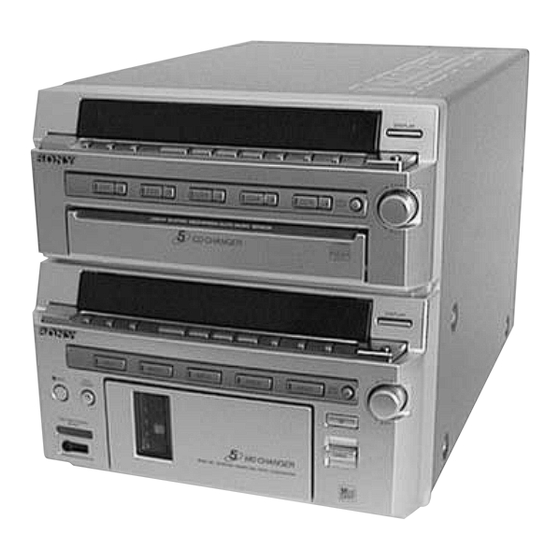
HMC-MD777
Model Name Using Similar Mechanism
CD Mechanism Type
CD
Section
Base Unit Name
Optical Pick-up Name
Model Name Using Similar Mechanism
MD Mechanism Type
MD
Section
Base Unit Name
Optical Pick-up Name
SPECIFICATIONS
CD PLAYER/MINI DISC DECK
E Model
NEW
CDM53-K1BD33
BU-K1BD33
KSM-213BFN
HCD-MD515
MDM-C1F
MBU-C1F
KMS-260B
Advertisement
Table of Contents

Related Manuals for Sony HMC-MD777


Summary of Contents for Sony HMC-MD777
- Page 1 HMC-MD777 SERVICE MANUAL E Model Ver. 1.2 2006.09 HMC-MD777 is the CD player and MD Deck section in DHC-MD777. Model Name Using Similar Mechanism U.S. and foreign patents licensed form Dolby Laboratories Licensing Corporation. CD Mechanism Type CDM53-K1BD33 Section Base Unit Name...
-
Page 2: Self-Diagnosis Function
SELF-DIAGNOSIS FUNCTION MD SECTION The self-diagnosis function consists of error codes for customers which are displayed automatically when errors occur, and error codes which show the error history in the test mode during servicing. For details on how to view error codes for the customer, refer to the following box in the instruction manual. - Page 3 Items of Error History Mode Items and Contents Display Details of History total rec Displays the recording time. Displayed as “rππππππh”. The displayed time is the total time the laser is set to the high power state. This is about 1/4 of the actual recording time. The time is displayed in decimal digits from 0h to 65535h.
- Page 4 (*2) NO DISC error code CD SECTION OPERATING THE DISPLAYED HISTORIES ** ** ** [PLAY MODE] [REPEAT] 1. Press the button simulta- neously, and the count of mechanical error and “NO DISC” that optical system judged are displyed. The number of NO DISC error. Emc= Edc= Latest one “00”...
-
Page 5: Table Of Contents
TABLE OF CONTENTS SELF-DIAGNOSIS FUNCTION ........2 SERVICING NOTES ..........6 GENERAL ..............13 DISASSEMBLY ............15 TEST MODE .............. 27 ELECTRICAL ADJUSTMENTS ......32 DIAGRAMS 6-1. Block Diagram – CD SERVO Section – ....... 41 6-2. Block Diagram – MD SERVO Section (1/2) – ..... 43 6-3. -
Page 6: Servicing Notes
COMPONENTS IDENTIFIED BY A ! MARK ON THE SCHEMATIC DIAGRAMS, EXPLODED VIEWS AND IN THE PARTS LIST ARE CRITICAL TO SAFE OPERATION. REPLACE THESE COMPO- NENTS WITH SONY PARTS WHOSE PART NUMBERS APPEAR AS SHOWN IN THIS MANUAL OR IN SUPPLEMENTS PUB- LISHED BY SONY. - Page 7 POWER SUPPLY DURING SERVICING • As this set has not own power supply, it does not operate inde- pendently. Therefore, during servicing, connect it to the Pre- Main amplifier and Tuner Unit (STR-MD777) of DHC-MD777. SYSTEM CONTROL terminal SYSTEM CONTROL terminal Pre-Main AMP and Tuner Unit Connector cable (15P)
- Page 8 MD SECTION IOP DATA RECORDING AND DISPLAY WHEN PICK-UP AND NON-VOLATILE MEMORY (IC171 ON BD (MD) BOARD) ARE REPLACED The IOP value labeled on the pick-up can be recorded in the non-volatile memory. By recording the value, it will eliminate the need to look at the value on the label of the optical pick-up.
- Page 9 AGING MODE Record 5 seconds repeat to each five discs. Note: Aging mode can not perform, if disconnect to the pre-main amplifier and tuner unit (STR-MD777) of DHC-MD777. Setting the Aging Mode 1. Insert recordable discs in all MD disc slots. [REC MODE] [REC] 2.
- Page 10 CHECKS PRIOR TO PARTS REPLACEMENT AND ADJUSTMENTS Before performing repairs, perform the following checks to determine the faulty locations up to a certain extent. Details of the procedures are described in “5 Electrical Adjustments”. Criteria for Determination Measure if unsatisfactory: (Unsatisfactory if specified value is not satisfied) Laser power check •...
- Page 11 CD SECTION CD-TEXT TEST DISC This unit is able to display the test data (character information) written in the CD on its fluorescent indicator tube. The CD-TEXT TEST DISC (TGCS-313: 4-989-366-01) is used for checking the display. To check, perform the following procedure. Checking Method: 1.
- Page 12 Table 2: CD-TEXT TEST DISC Recorded Contents and Display (In this unit, some special characters cannot be displayed. This is no a fault.) TRACK Recorded contents Display N All the same ! ” # $ % & ´ (21h to 27h)1kHz 0dB L&R + , –...
-
Page 13: General
SECTION 2 GENERAL LOCATION OF CONTROLS – Front Panel – 1 1/ALL button • CD PLAYER Section 2 PLAY MODE button 4 5 6 7 3 REPEAT button 4 fl button !º 5 π button !¡ 6 0 button !™ 7 ) button !£... - Page 14 – REAR PANEL – 1 CD ANALOG OUT jack 2 MD ANALOG IN/OUT jack 3 OPTICAL IN, DIGITAL IN connector 4 SYSTEM CONTROL terminal – 14 –...
-
Page 15: Disassembly
SECTION 3 DISASSEMBLY • This set can be disassembled in the order shown below. Case (Page 16) Front Panel Section (Page 16) CD Mechanism Deck Section (CDM53-K1BD33) (Page 17) RELAY Board CD Base Unit (BU-K1BD33) Fitting Base (Guide/Magnet) Ass’y (Page 17) (Page 19) (Page 19) Tray (Sub) - Page 16 Note: Follow the disassembly procedure in the numerical order given. CASE 3 case 1 three screws (BVTT3 × 6) 2 three screws (case 3TP2) 2 three screws (case 3TP2) FRONT PANEL SECTION 1 wire (flat type) (21 core) 5 connector (CN691) (CN1) 4 front panel section...
- Page 17 CD MECHANISM DECK SECTION (CDM53-K1BD33) 5 Remove the CD mechanism deck section (CDM53-K1BD33) in the direction of the arrow. 4 two screws 3 four screws (BV3 × 8) (BV3 × 8) 6 wire (flat type) (19 core) (CN300) 1 connector (CN713) 2 wire (flat type) (17 core) (CN701)
- Page 18 MD MECHANISM DECK SECTION (MDM-C1F) 3 connector 1 four screws (CN106) (BV3 × 8) 2 MD mechanism deck section (MDM-C1F) MICROCOMPUTER BOARD, MAIN BOARD 2 PWB holder 3 Remove the MICROCOMPUTER board in the direction of the arrow. 5 screw (BV3 ×...
- Page 19 CD BASE UNIT (BU-K1BD33) 2 CD base unit (BU-K1BD33) 1 two screws 1 two screws (PTPWHM2.6) (PTPWHM2.6) FITTING BASE (GUIDE/MAGNET) ASS’Y 7 four screws (BVTP2.6) 5 bracket (chassis) 2 four screws (BVTP2.6) 4 two screws (BVTP2.6) 6 connector (CN710) 8 fitting base (magnet) ass’y 4 two screws (BVTP2.6) 3 fitting base (guide) ass’y...
- Page 20 TRAY (SUB) 1 Rotate the pulley (LD) and move the slider (selection) in the direction of the arrow L . 2 Rotate the pulley (mode) in the direction of the arrow and adjust the tray (sub) of object. 3 Rotate the pulley (LD) and move the slider (selection) in the direction of the arrow R .
- Page 21 INSTALLATION OF GEARS 3 gear (gear B) part A Adjust the gear with Rof part A in the figure. 1 Move the slider (U/D) in the direction of the arrow fully. 4 gear (gear A) 2 gear (U/D slider) gear (gear B) gear of slider (U/D) a straight line Install the gear (gear A)
- Page 22 INSTALLATION OF STOCKER 2 part A of tray (sub) Hang the part A of tray (sub) 1 stocker on the slider (selection). part A of tray (sub) part A of claw of slider tray (sub) (selection) 3 two step screws 3 two step screws INSTALLATION OF CHASSIS (MOLD B) 3 three screws...
- Page 23 ESCUTCHEON (’98 FRONT), CHASSIS (TOP) 4 two screws (BVTT2.6 × 5) 6 screw (BVTT2.6 × 5) 5 cover (FFC) 8 bracket (Refer to note for installation of bracket when install.) 9 two screws (P2 × 5) !º chassis (top) 3 wire (flat type) (13 core) (CN552) 3 wire (flat type) (7 core) (CN551)
- Page 24 CHASSIS (ELEVATOR) (NEW) ASS’Y 1 Remove the chassis (elevator) (new) ass’y in the direction of the arrow. MOTOR (HEAD) ASS’Y (M4), HEAD RELAY BOARD 7 Break the soldering of motor. 8 HEAD RELAY board 1 connector (CNP19) 3 screw (BVTT2.6 × 5) 6 Revove the motor (head) ass’y (M4) in the direction of the arrow B .
- Page 25 MD BASE UNIT (MBU-C1F) over write head 1 two step screws 1 two step screws 2 MD base unit (MBU-C1F) 3 connector (CB108) chassis (elevaor) Take care not to catch. BD (MD) BOARD 3 two screws (P1.7 × 2.2) 2 connector (CN109) 6 flexible board (CN101)
- Page 26 OVER WRITE HEAD (HR901) 1 screw (P1.7 × 2.5) 2 over write head (HR901) OPTICAL PICK-UP (KMS-260B/J1N) (for MD) 4 Remove the optical pick-up (KMS-260B/J1N) (for MD) in the direction of the arrow. 1 screw (M1.7 × 1.4) 2 stopper 3 shaft (main) –...
-
Page 27: Test Mode
SECTION 4 TEST MODE 1. PRECAUTIONS FOR USE OF TEST MODE • As loading related operations will be performed regardless of the test mode operations being performed, be sure to check that the disc is stopped before setting and removing it. Even if the §... - Page 28 5. SELECTING THE TEST MODE There are 31 types of test modes as shown below. The groups can be switched by turning the ≠↔± dial. After selecting the group [ENTER/YES] button. After setting a certain group, turning the ≠↔± dial switches between these modes. to be used, press the Refer to “Group”...
- Page 29 5-1. Operating the Continuous Playback Mode 1. Entering the continuous playback mode (1) Set the disc in the unit. (Whichever recordable discs or discs for playback only are available) (2) Turn the ≠↔± dial to display “CPLAY MODE” (C30). [ENTER/YES] (3) Press the button to change the display to “CPLAY MID”.
- Page 30 6. FUNCTIONS OF OTHER BUTTONS Function Contents Sets continuous playback when pressed in the STOP state. When pressed during continuous playback, the tracking servo · turns ON/OFF. π Stops continuous playback and continuous recording. The sled moves to the outer circumference only when this is pressed. The sled moves to the inner circumference only when this is pressed.
- Page 31 MEANINGS OF OTHER DISPLAYS Contents Display When Off When Light · During continuous playback (CLV: ON) STOP (CLV: OFF) Tracking servo OFF Tracking servo ON Recording mode ON Recording mode OFF SYNC CLV low speed mode CLV normal mode L-SYNC ABCD adjustment completed OVER Tracking offset cancel ON...
-
Page 32: Electrical Adjustments
SECTION 5 ELECTRICAL ADJUSTMENTS 4. Use the following tools and measuring devices. MD SECTION • Extension cable (19P) (Part No. J-2501-011-B) Relay connector (Part No. J-2501-167-A) 1. PRECAUTIONS FOR CHECKING LASER DIODE (BD (CD) board CN101 to MICROCOMPUTER board EMISSINON CN300) To check the emission of the laser diode during adjustments, never •... - Page 33 [ENTER/YES] 5. CHECK PRIOR TO REPAIRS Note 1: After step 4, each time the button is pressed, the display will be switched between “LD 0.7 mW $ ”, “LD These checks are performed before replacing parts according to 6.2 mW $ ”, and “LD Wp ”.
- Page 34 [ENTER/YES] 5-4. Focus Bias Check 9. Press the button to display “EFB = MO-P”. Then, the optical pick-up moves to the pit area automatically Change the focus bias and check the focus tolerance amount. and servo is imposed. Checking Procedure : 10.
- Page 35 6. INITIAL SETTING OF ADJUSTMENT VALUE 8. TEMPERATURE COMPENSATION OFFSET ADJUTMENT Note: Save the temperature data at that time in the non-volatile memory Mode which sets the adjustment results recorded in the non-volatile as 25 ˚C reference data. memory to the initial setting value. However the results of the tempera- Note : ture compensation offset adjustment will not change to the initial setting 1.
- Page 36 7. Then, turn the ≠↔± dial to display “LDPWR 10. TRAVERSE ADJUSTMENT CHECK” (C02). [ENTER/YES] Note 1:Data will be erased during MO reading if a recorded disc is 8. Press the button once to display “LD 0.9 mW used in this adjustment. ”.
- Page 37 [ENTER/YES] 8. Turn the ≠↔± dial so that the waveform of the oscil- 18. Press the button, display “EFB = SAVE” loscope becomes the specified value. for a moment and save the adjustment results in the non-vola- (When the ≠↔± dial is turned, the of “EFB- ”...
- Page 38 12. ERROR RATE CHECK 14. AUTO GAIN CONTROL OUTPUT LEVEL 12-1. CD Error Rate Check ADJUSTMENT Checking Procedure : Be sure to perform this adjustment when the pickup is replaced. 1. Load a check disc (MD) TDYS-1. If the adjustment results becomes “Adjust NG!”, the pickup may 2.
- Page 39 RF signal waveform CD SECTION VOLT/DIV: 200 mV Note: TIME/DIV: 500 ns 1. CD Block is basically designed to operate without adjustment. There- fore, check each item in order given. 2. Use YEDS-18 disc (3-702-101-01) unless otherwise indicated. level: 1.2 ± 0.2 Vp-p 3.
- Page 40 Connecting points: [BD (MD) Board] (Side A) [BD (MD) Board] (Side B) CN101 TP167 D101 TP233 IC101 (VC) (TEO) TP170 IC124 (I+3V) TP169 (IOP) [BD (CD) Board] (Side B) [MICROCOMPUTER Board] (Side B) TP308 (ADJ) IC102 (VC) (AGCCON) (FEO) (RF) IC101 IC300 TP (VC)
-
Page 41: Diagrams
HMC-MD777 SECTION 6 DIAGRAMS 6-1. BLOCK DIAGRAM – CD SERVO Section – FILTER DIGITAL SIGNAL PROCESSOR, DIGITAL FILTER, D/A CONVERTER IC101 (1/2) RF AMP, 56 53 FOCUS/TRACKING ERROR AMP IC103 DETECTOR D+5V PCMD LRCK INTERFACE C2PO RFAC RF EQ ASYMMETRY... -
Page 42: Block Diagram - Md Servo Section (1/2)
HMC-MD777 6-2. BLOCK DIAGRAM – MD SERVO Section (1/2) – IC121 (1/2) OVER WRITE EFMO ADDT ADDT (Page 45) HEAD DRIVE IC181, Q181, 182 DATAI HR901 DIGITAL SIGNAL PROCESSOR, FILI SAMPLING OVER WRITE HEAD SCTX XBCKI EFM/ACIRC ENCODER/DECODER, RATE SHOCK PROOF MEMORY CONTROLLER,... - Page 43 HMC-MD777 6-3. BLOCK DIAGRAM – MD SERVO Section (2/2) – S681 LIMIT-IN (LIMIT) A/D, D/A CONVERTER IC201 S682 REFLECT J901 (2/2) (REFLECT) S683 PROTECT 59 VINL1 (PROTECT) ADDT DATAO DIGITAL MIXER, DECIMATION VINL2 (Page 44) DIGITAL AGC FILTER MD ANALOG IN...
-
Page 44: Block Diagram - Display/Power Supply Section
HMC-MD777 6-4. BLOCK DIAGRAM – DISPLAY/POWER SUPPLY Section – MASTER CONTROLLER FLUORESCENT (CD MECHANISM CONTROLLER) LED DRIVER FL DRIVER INDICATOR TUBE IC300 (2/2) FL601 IC661 IC601 S604, 613, D661 – 665 KEY0 S661 – 665 SDATA DRVDAT DATA DRVCLK DRVCS... -
Page 45: Note For Printed Wiring Boards And Schematic Diagrams
• Circuit Boards Location 6-5. NOTE FOR PRINTED WIRING BOARDS AND SCHEMATIC DIAGRAMS CD SW board Note on Printed Wiring Board: Note on Schematic Diagram: MICROCOMPUTER board • X : parts extracted from the component side. • All capacitors are in µF unless otherwise noted. pF: µµF CONNECTOR board •... - Page 46 HMC-MD777 6-6. PRINTED WIRING BOARD – BD (CD) Section – • See Page 49 for Circuit Boards Location. (Page 72) • Semiconductor • Semiconductor Location Location (SIDE A) (SIDE B) Ref. No. Location Ref. No. Location Q101 IC101 IC102 IC103 –...
- Page 47 HMC-MD777 6-7. SCHEMATIC DIAGRAM – BD (CD) Section – • See page 65 for Waveforms. • See page 99 for IC Block Diagrams. (Page 73) The components identified by mark ! or dotted line with mark ! are critical for safety.
- Page 48 HMC-MD777 6-8. PRINTED WIRING BOARDS – CD MOTOR/SENSOR Section – • See page 49 for Circuit Boards Location. (Page 55) (Page 56) (Page 55) (Page 72) (Page 56) (Page 72) – 55 – – 56 –...
- Page 49 HMC-MD777 6-9. SCHEMATIC DIAGRAM – CD MOTOR/SENSOR Section – • See page 100 for IC Block Diagram. (Page 73) (Page 73) – 57 – – 58 –...
-
Page 50: Schematic Diagram - Bd (Md) Section (1/2)
HMC-MD777 6-10. SCHEMATIC DIAGRAM – BD (MD) Section (1/2) – • See page 65 for Waveforms. • See page 101 for IC Block Diagrams. (Page (Page 78) (Page 62) (Page 81) (Page 62) The components identified by mark ! or dotted line with mark ! are critical for safety. -
Page 51: Schematic Diagram - Bd (Md) Section (2/2)
HMC-MD777 6-11. SCHEMATIC DIAGRAM – BD (MD) Section (2/2) – • See page 66 for Waveform. (Page 70) (Page (Page 69) (Page 69) (Page (Page 77) (Page 60) (Page 59) – 61 – – 62 –... - Page 52 HMC-MD777 6-12. PRINTED WIRING BOARDS – BD (MD) Section – • See page 49 for Circuit Boards Location. (Page 76) (Page 67) (Page 76) (Page 68) (Page 68) (Page 80) (Page 68) • Semiconductor Location • Semiconductor Location (SIDE A) (SIDE B) Ref.
- Page 53 • Waveforms – BD (CD) Board – – BD (MD) Board – – MICROCOMPUTER Board – – MD DISPLAY Board – 1 IC103 !§ (RF O) (CD Play Mode) 5 IC101 ^§ (XTAI) 1 IC101 #• (RF) (MD Play Mode) 5 IC121 @•...
-
Page 54: Printed Wiring Boards - Md Motor/Sensor Section
HMC-MD777 6-13. PRINTED WIRING BOARDS – MD MOTOR/SENSOR Section – • See page 49 for Circuit Boards Location. (Page 63) (Page 63) (Page 63) (Page 68) (Page 64) (Page 67) – 67 – – 68 –... -
Page 55: Schematic Diagram - Md Motor/Sensor Section
HMC-MD777 6-14. SCHEMATIC DIAGRAM – MD MOTOR/SENSOR Section – • See page 103 for IC Block Diagram. (Page 62) (Page 62) (Page 61) (Page 62) – 69 – – 70 –... -
Page 56: Printed Wiring Board - Microcomputer Section
HMC-MD777 6-15. PRINTED WIRING BOARD – MICROCOMPUTER Section – • See page 49 for Circuit Boards Location. (Page 56) MICROCOMPUTER BOARD MICROCOMPUTER BOARD (SIDE A) (SIDE B) (Page 52) (Page 56) (Page 80) (Page 79) • Semiconductor Location Ref. No. - Page 57 HMC-MD777 6-16. SCHEMATIC DIAGRAMS – MICROCOMPUTER Section – • See page 66 for Waveform. (Page 81) (Page (Page 81) (Page 81) (Page (Page (Page • Voltages and waveforms are dc with respect to ground under no-signal conditions. no mark : CD PLAY ∗...
-
Page 58: Printed Wiring Boards - Relay Section
HMC-MD777 6-17. PRINTED WIRING BOARDS – RELAY Section – • See page 49 for Circuit Boards Location. (Page 64) (Page 91) (Page 64) RELAY BOARD LINK (Page 80) • Semiconductor Location Ref. No. Location IC401 IC402 IC451 Q400 Q401 Q403 Q404 –... -
Page 59: Schematic Diagram - Relay Section
HMC-MD777 6-18. SCHEMATIC DIAGRAM – RELAY Section – • See page 103 for IC Block Diagram. (Page 62) (Page 60) (Page 93) (Page 81) • Voltages are dc with respect to ground under no-signal conditions. no mark : CD PLAY ) : MD PLAY –... -
Page 60: Printed Wiring Board - Main Section
HMC-MD777 6-19. PRINTED WIRING BOARD – MAIN Section – • See page 49 for Circuit Boards Location. (Page 75) (Page 72) • Semiconductor Location Ref. No. Location D001 D002 D003 D004 D201 CD ANALOG OUT D202 D203 D204 D205 D206... -
Page 61: Schematic Diagram - Main Section
HMC-MD777 6-20. SCHEMATIC DIAGRAM – MAIN Section – • See page 104 for IC Block Diagram. (Page (Page 78) (Page 74) (Page 74) (Page 74) • Voltages are dc with respect to ground under no-signal conditions. no mark : CD PLAY –... -
Page 62: Printed Wiring Boards - Cd Jog/Sw Section
HMC-MD777 6-21. PRINTED WIRING BOARDS – CD JOG/SW Section – • See page 49 for Circuit Boards Location. (SIDE A) • Semiconductor (SIDE B) Location Ref. No. Location D661 D662 D663 D664 D665 IC661 (page 83) (page 88) (SIDE A) -
Page 63: Schematic Diagram - Cd Jog/Sw Section
HMC-MD777 6-22. SCHEMATIC DIAGRAM – CD JOG/SW Section – • See page 104 for IC Block Diagram. (page 74) (page 98) • Voltages are dc with respect to ground under no-signal conditions. no mark : CD1 PLAY/CD2 STOCK – 85 –... -
Page 64: Printed Wiring Board - Cd Display Section
HMC-MD777 6-23. PRINTED WIRING BOARD – CD DISPLAY Section – • See page 49 for Circuit Boards Location. (page 84) – 87 – – 88 –... -
Page 65: Schematic Diagram - Cd Display Section
HMC-MD777 6-24. SCHEMATIC DIAGRAM – CD DISPLAY Section – • See page 66 for Waveforms. • See page 104 for IC Block Diagarm. (page 86) • Voltages and waveforms are dc with respect to ground under no-signal conditions. no mark : CD STOP –... -
Page 66: Printed Wiring Boards - Md Jog/Sw Section
HMC-MD777 6-25. PRINTED WIRING BOARDS – MD JOG/SW Section – • See page 49 for Circuit Boards Location. (SIDE A) • Semiconductor Location Ref. No. Location (SIDE B) D801 (page 96) D802 D803 D804 D805 D806 D807 D808 IC802 Q802... -
Page 67: Schematic Diagram - Md Jog/Sw Section
HMC-MD777 6-26. SCHEMATIC DIAGRAM – MD JOG/SW Section – • See page 104 for IC Block Diagram. (page 98) (page 77) • Voltages are dc with respect to ground under no-signal conditions. no mark : MD1 PLAY/MD2 STOCK – 93 –... -
Page 68: Printed Wiring Board - Md Display Section
HMC-MD777 6-27. PRINTED WIRING BOARD – MD DISPLAY Section – • See page 49 for Circuit Boards Location. (page 84) (page 92) – 95 – – 96 –... -
Page 69: Schematic Diagram - Md Display Section
HMC-MD777 6-28. SCHEMATIC DIAGRAM – MD DISPLAY Section – • See page 66 for Waveforms. (page 93) (page 86) • Voltages and waveforms are dc with respect to ground under no-signal conditions. no mark : MD STOP – 97 –... - Page 70 • IC Block Diagrams IC103 CXA2568M-T6 – BD (CD) BOARD – IC101 CXD2587Q HOLD APC PD AMP LC/PD APC LD AMP – LD ON – – ERROR – DIGITAL CORRECTOR DIGITAL ASYMMETRY CORRECTION HOLD SW AGC CONT OPERATIONAL LRCK AMPLIFIER AGC VTH 50µA ANALOG SWITCH...
- Page 71 – BD (MD) BOARD – IC101 CXA2523AR 43 42 USROP – RF AGC – USRC RFA1 BPF3T RFA2 RFA3 PEAK3T – HLPT –1 – – –2 – OFST PTGR TEMP PEAK – –2 – 36 BOTM BOTTOM – –1 GRVA PBSW 35 ABCD 34 FE...
- Page 72 IC121 CXD2654R 100 99 98 97 96 95 94 93 92 91 90 89 88 87 86 85 84 83 82 81 80 79 78 77 76 SPINDLE GENERATOR SERVO 75 TE MNT0 74 SE MNT1 EACH MONITOR 73 AVSS BLOCK CONTROL MNT2...
- Page 73 IC172 BA6287F OUT1 OUT2 DRIVER DRIVER VREF CONTROL LOGIC POWER SAVE IC201 UDA1341TS/N2 VSS(AD) 1 VREF 0dB/6dB ADC1L VINL1 2 VSS(DAC) SWITCH VDD(AD) 3 VOUTL 0dB/6dB DIGITAL ADC1R VINR1 4 VDD(DAC) SWITCH INTERFACE VADCN 5 VOUTR VINL2 6 ADC2L DIGITAL VADCP 7 VINR2 8 ADC2R...
- Page 74 – MAIN BOARD – – CD JOG BOARD/MD JOG BOARD – IC204 P82B715PN IC661 NJU3718G (TE2) (CD JOG Board) IC802 NJU3718G (TE2) (MD JOG Board) DIG11 DIG12 DIGITAL OUTPUT BUFFER DIG0 DIG15 CIRCUIT BUFFER INDICATION SERIAL CONTROLLER RECEIVE CIRCUIT DATA INDICATION OUTPUT CONTROL...
-
Page 75: Ic Pin Function Description
6-29. IC PIN FUNCTION DESCRIPTION • BD (MD) BOARD IC101 CXA2523AR (RF AMP, FOCUS/TRACKING ERROR AMP) Pin No. Pin Name Function I-V converted RF signal I input from the optical pick-up block detector I-V converted RF signal J input from the optical pick-up block detector Middle point voltage (+1.65V) generation output terminal 4 to 9 A to F... - Page 76 • BD (MD) BOARD IC121 CXD2654R (DIGITAL SIGNAL PROCESSOR, DIGITAL SERVO PROCESSOR, EFM/ACIRC ENCODER/DECODER, SHOCK PROOF MEMORY CONTROLLER, ATRAC ENCODER/DECODER) Pin No. Pin Name Function Focus OK signal output to the MD mechanism controller (IC316) MNT0 (FOK) “H” is output when focus is on (“L”: NG) MNT1 (SHOCK) Track jump detection signal output to the MD mechanism controller (IC316) MNT2 (XBUSY)
- Page 77 Pin No. Pin Name Function Address signal output to the D-RAM (IC124) XRAS Row address strobe signal output to the D-RAM (IC124) “L” active Write enable signal output to the D-RAM (IC124) “L” active Two-way data bus with the D-RAM (IC124) I (S) MVCI Digital in PLL oscillation input from the external VCO Not used (fixed at “L”)
- Page 78 Pin No. Pin Name Function SRDR Sled servo drive PWM signal (–) output to the BH6511FS (IC152) SFDR Sled servo drive PWM signal (+) output to the BH6511FS (IC152) SPRD Spindle servo drive PWM signal (–) output to the BH6511FS (IC152) SPFD Spindle servo drive PWM signal (+) output to the BH6511FS (IC152) I (S)
- Page 79 • BD (MD) BOARD IC316 M30624MG-205B (MD MECHANISM CONTROLLER) Pin No. Pin Name Function WMOUT Serial data output to the equipment connected to MD WALKMAN LINK jack (J1) Serial data transfer clock signal input from the equipment connected to MD WALKMAN LINK WMCLK jack (J1) LEVEL-L...
- Page 80 Pin No. Pin Name Function SCLK Serial clock signal output to the CXD2654R (IC121) OPTSEL0 Selection signal output for the optical input signal Not used (open) SENSOR Elevator position detect sensor (PH570) input terminal SENSOR2 Elevator position detect sensor (PH571) input terminal Over write head up/down motor control signal output to the motor driver IC (IC172) HEADDOWN “H”...
- Page 81 Pin No. Pin Name Function Laser modulation select signal output to the HF module switch circuit Playback power: “H”, Stop: “L”, Recording power: 0.5 sec 2 sec XLATCH Serial data latch pulse signal output to the CXD2654R (IC121) Laser power select signal output to the CXD2654R (IC121) and HF module switch circuit WRPWR “L”: playback mode, “H”: recording mode LOADING...
- Page 82 Pin No. Pin Name Function Key input terminal (A/D input) KEY1 S603, S604, S606 to S609 (PLAY MODE, REPEAT, π, fl, 0, )) keys input AVSS — Ground terminal (for A/D converter) Key input terminal (A/D input) S602, S610 to S613, S802 (1/ALL, NAME EDIT, MENU/NO, KEY0 ENTER/YES, CLEAR, DISPLAY) keys input VREF...
- Page 83 • MICROCOMPUTER BOARD IC300 µPD784215AYGF-501-3BA (MASTER CONTROLLER (CD MECHANISM CONTROL)) Pin No. Pin Name Function 1, 2 OPEN Not used (open) LEDLAT Serial data latch pulse output to the LED driver IC (IC661) DRVCS Chip select signal output to the FL driver IC (IC601) “L” active Output enable signal output to the static RAM (IC302) “L”...
- Page 84 Pin No. Pin Name Function BUSD0 CD digital signal selection control signal output terminal BUSD1 Not used (open) BUSD2 Not used (open) I2CHELP Busy signal output for the I2C bus “L” active (BUSD3) — Power supply terminal (+5V) Main system clock output terminal (12.5 MHz) Main system clock input terminal (12.5 MHz) —...
- Page 85 Pin No. Pin Name Function LPH (XMODE) Laser power control signal output to the CXA2568M (IC103) on the CD block SENSE2 Monitor detection signal input of the internal status Not used (open) I2CDATA Data input/output terminal for the I2C bus SENSE Internal status detection monitor input from the CXD2587Q (IC101) on the CD block I2CCLK...
-
Page 86: Exploded Views
SECTION 7 EXPLODED VIEWS NOTE: • -XX and -X mean standardized parts, so they • Items marked “*” are not stocked since they The components identified by mark ! or dotted line with mark may have some difference from the original are seldom required for routine service. - Page 87 (2) FRONT PANEL SECTION supplied supplied supplied supplied supplied Ref. No. Part No. Description Remark Ref. No. Part No. Description Remark X-4950-483-1 PANEL ASSY, FRONT * 67 A-4724-393-A CD JOG BOARD, COMPLETE X-4950-488-1 LID (MD) ASSY 4-951-620-11 SCREW (2.6X10), +BVTP * 53 4-930-336-71 FOOT (FELT) * 69...
- Page 88 (3) CHASSIS SECTION SS202 supplied supplied supplied supplied supplied supplied supplied Ref. No. Part No. Description Remark Ref. No. Part No. Description Remark * 101 3-346-265-11 HOLDER, PC BOARD 1-790-266-11 WIRE (FLAT TYPE) (17 CORE) * 102 A-4724-389-A MAIN BOARD, COMPLETE * 106 4-213-359-11 PANEL, BACK 1-790-268-11 WIRE (FLAT TYPE) (21 CORE)
- Page 89 (4) CD MECHANISM DECK SECTION-1 (CDM53-K1BD33) (including not supplied not supplied M702 Ref. No. Part No. Description Remark Ref. No. Part No. Description Remark 4-951-620-41 SCREW (2.6), +BVTP * 164 1-671-505-11 IN SW BOARD * 152 1-671-508-11 LOAD MOTOR BOARD A-4672-623-C BASE (MAGNET) ASSY, FITTING 4-211-215-01 GEAR (EJECT) * 166...
- Page 90 (5) CD MECHANISM DECK SECTION-2 (CDM53-K1BD33) not supplied not supplied S707 not supplied M701 not supplied BU-K1BD33 Ref. No. Part No. Description Remark Ref. No. Part No. Description Remark 4-985-672-01 SCREW (+PTPWH M2.6), FLOATING 4-212-677-01 SLIDER (SHUTTER) 4-211-871-11 INSULATOR (M) (BLUE) 4-212-678-01 SPRING (SHUTTER), TENSION 4-211-871-01 INSULATOR (M) (BLACK) 4-211-233-01 SLIDER (SELECTION)
- Page 91 Ver. 1.1 (6) CD BASE UNIT SECTION (BU-K1BD33) not supplied not supplied not supplied M102 The components identified by mark 0 or dotted line with mark 0 are critical for safety. Replace only with part number specified. Ref. No. Part No. Description Remark Ref.
- Page 92 (7) MD MECHANISM DECK SECTION-1 (MDM-C1F) not supplied not supplied not supplied MBU-C1F Ref. No. Part No. Description Remark Ref. No. Part No. Description Remark 4-987-327-01 INSULATOR 3-701-438-21 WASHER (E-2.3), NYLON 4-987-240-01 SCREW, STEP 3-018-636-01 GEAR (PULLEY) (C) 4-986-932-01 HOLDER (R) 3-018-203-01 GEAR (HEAD) (A) 4-212-592-01 ESCUTCHEON (’98 FRONT) 3-018-204-01 GEAR (HEAD) (B)
- Page 93 (8) MD MECHANISM DECK SECTION-2 (MDM-C1F) S573 S572 M572 M571 353 352 Ref. No. Part No. Description Remark Ref. No. Part No. Description Remark 4-986-951-01 GEAR (4) * 368 1-671-469-11 ELEVATOR RELAY BOARD 4-987-243-01 BELT, TOOTHED LOCK 1-782-909-11 WIRE (FLAT TYPE) (13 CORE) 4-986-947-01 STOPPER X-4947-928-1 BRACKET (1A) ASSY 3-701-438-21 WASHER (E-2.3), NYLON...
- Page 94 (9) MD BASE UNIT SECTION (MBU-C1F) M681 HR901 M682 The components identified by mark ! or dotted line with mark ! are critical for safety. Replace only with part number specified. Ref. No. Part No. Description Remark Ref. No. Part No. Description Remark * 401...
-
Page 95: Electrical Parts List
SECTION 8 BD (CD) ELECTRICAL PARTS LIST NOTE: The components identified by • Due to standardization, replacements in the • Items marked “*” are not stocked since they mark ! or dotted line with mark are seldom required for routine service. ! are critical for safety. - Page 96 BD (CD) BD (MD) Ref. No. Part No. Description Remark Ref. No. Part No. Description Remark R119 1-216-041-00 METAL CHIP 1/10W C123 1-163-038-00 CERAMIC CHIP 0.1uF R123 1-216-073-00 METAL CHIP 1/10W R124 1-216-097-00 RES,CHIP 100K 1/10W C124 1-163-038-00 CERAMIC CHIP 0.1uF R131 1-216-037-00 METAL CHIP...
- Page 97 BD (MD) Ref. No. Part No. Description Remark Ref. No. Part No. Description Remark C503 1-125-822-11 TANTALUM 10uF L401 1-414-813-11 FERRITE C509 1-125-822-11 TANTALUM 10uF L502 1-414-813-11 FERRITE C510 1-125-822-11 TANTALUM 10uF C522 1-163-038-00 CERAMIC CHIP 0.1uF < TRANSISTOR > C527 1-163-038-00 CERAMIC CHIP 0.1uF...
- Page 98 BD (MD) Ref. No. Part No. Description Remark Ref. No. Part No. Description Remark R167 1-216-065-00 RES,CHIP 4.7K 1/10W R802 1-216-025-00 RES,CHIP 1/10W R169 1-219-724-11 METAL CHIP 1/4W R803 1-216-025-00 RES,CHIP 1/10W R170 1-216-073-00 METAL CHIP 1/10W R171 1-216-073-00 METAL CHIP 1/10W R804 1-216-025-00 RES,CHIP...
- Page 99 BD (MD) CD DISPLAY CD JOG Ref. No. Part No. Description Remark Ref. No. Part No. Description Remark R1002 1-216-001-00 METAL CHIP 1/10W < TRANSISTOR > R1003 1-216-001-00 METAL CHIP 1/10W R2000 1-216-073-00 METAL CHIP 1/10W Q601 8-729-620-05 TRANSISTOR 2SC2603-EF R2001 1-216-073-00 METAL CHIP 1/10W...
- Page 100 CD JOG CD SW CLAMP MOTOR CONNECTOR CONNECTOR (CD) DISC SW Ref. No. Part No. Description Remark Ref. No. Part No. Description Remark R675 1-216-041-00 METAL CHIP 1/10W S613 1-771-544-11 SWITCH, TACTILE (CLEAR) ************************************************************ R676 1-216-045-00 METAL CHIP 1/10W R677 1-216-049-11 RES,CHIP 1/10W 1-671-507-11 CLAMP MOTOR BOARD...
- Page 101 Ver. 1.2 DISC SW ELEVATOR RELAY HEAD RELAY HEAD SW INIT/COUNT SW IN SW LOAD MOTOR Ref. No. Part No. Description Remark Ref. No. Part No. Description Remark < SWITCH > 1-671-470-11 HEAD RELAY BOARD ***************** 1-771-225-12 SWITCH, LEVER (DISC 1) 1-771-225-12 SWITCH, LEVER (DISC 2) <...
- Page 102 LOAD MOTOR MAIN Ref. No. Part No. Description Remark Ref. No. Part No. Description Remark < RESISTOR > C951 1-126-964-11 ELECT 10uF C952 1-164-159-11 CERAMIC 0.1uF R703 1-249-411-11 CARBON 1/4W C953 1-126-059-11 ELECT 10uF R704 1-249-401-11 CARBON 1/4W C954 1-106-359-00 MYLAR 4700PF 200V ************************************************************...
- Page 103 MAIN MD DISPLAY Ref. No. Part No. Description Remark Ref. No. Part No. Description Remark < FERRITE BEAD > R215 1-260-096-11 CARBON 1/2W R216 1-249-422-11 CARBON 2.7K 1/4W FB201 1-410-397-21 FERRITE BEAD INDUCTOR R217 1-249-429-11 CARBON 1/4W FB204 1-410-397-21 FERRITE BEAD INDUCTOR FB205 1-410-397-21 FERRITE BEAD INDUCTOR R218...
- Page 104 MD DISPLAY MD JOG Ref. No. Part No. Description Remark Ref. No. Part No. Description Remark < CAPACITOR > < SWITCH > C801 1-162-282-31 CERAMIC 100PF S802 1-762-875-21 SWITCH, KEYBOARD (DISPLAY) C802 1-162-282-31 CERAMIC 100PF ************************************************************ C803 1-162-282-31 CERAMIC 100PF C804 1-162-282-31 CERAMIC 100PF...
- Page 105 MD JOG MD SW MECH RELAY MICROCOMPUTER Ref. No. Part No. Description Remark Ref. No. Part No. Description Remark R833 1-216-057-00 METAL CHIP 2.2K 1/10W S608 1-771-544-11 SWITCH, TACTILE (0) R834 1-216-061-00 METAL CHIP 3.3K 1/10W S609 1-771-544-11 SWITCH, TACTILE ()) R835 1-216-065-91 RES,CHIP 4.7K...
- Page 106 MICROCOMPUTER Ref. No. Part No. Description Remark Ref. No. Part No. Description Remark < CONNECTOR > R314 1-216-065-00 RES,CHIP 4.7K 1/10W R315 1-216-065-00 RES,CHIP 4.7K 1/10W CN300 1-784-741-11 CONNECTOR, FFC 19P R316 1-216-073-00 METAL CHIP 1/10W CN301 1-784-739-11 CONNECTOR, FFC 17P R317 1-216-073-00 METAL CHIP 1/10W...
- Page 107 MICROCOMPUTER OUT SW RELAY SENSOR Ref. No. Part No. Description Remark Ref. No. Part No. Description Remark R394 1-216-065-00 RES,CHIP 4.7K 1/10W < CONNECTOR > R395 1-216-065-00 RES,CHIP 4.7K 1/10W CN401 1-564-723-11 PIN, CONNECTOR (SMALL TYPE) 7P < VIBRATOR > CN451 1-784-745-11 CONNECTOR, FFC 23P CN453...
- Page 108 HMC-MD777 Ver. 1.1 SENSOR SENSOR 2 Ref. No. Part No. Description Remark Ref. No. Part No. Description Remark < LED > 1-790-266-11 WIRE (FLAT TYPE) (17 CORE) 0 253 A-3328-818-A OPTICAL PICK-UP (KSM-213BFN) (for CD) D704 8-719-055-84 LED GL-528VS1 (DISC IN DETECT SENSOR)
Need help?
Do you have a question about the HMC-MD777 and is the answer not in the manual?
Questions and answers