Alinco DR-M03R Service Manual
Hide thumbs
Also See for DR-M03R:
- Instruction manual (55 pages) ,
- Service manual (34 pages) ,
- Instruction manual (55 pages)
Table of Contents
Advertisement
Quick Links
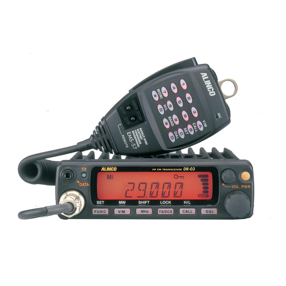
DR-M03R I DR-03T
S e r v i c e M a n u a l
C O N T E N T S
GENERAL............................ ...................... ............. 2
TRANSMITTER.................... .................................2
RECEIVER....................................................... ....... 2
1) Receiver System....................
2) Transmitter System ............................................4
3) PLL Synthesizer Circuit.........
4) CPU and Peripheral Circuit............... ...................5,6
5)
Power Supply Circuit............................ ......... ........6
6)
M38268MCA082GP#U0 (XA1170A)..... ........
1) NJM7808FA(XA0102)................. .......... ............. 10
2) . TC4S66F (XA0115)......................................... .......10
3) TC4W53FU (XA0348)..............
4) TA31136FN (XA0404)............................ ......... ...... 11
5)
LA4425A (XA0410)......................
6)
BR24L32FJ (XA0604Z)...........................................12
7) S-80845ALMP (XA0620)............. .............. ...........12
8)
N JM78M05DL1A (XA0947)................. .................. 12
9)
MB15A01PFV1 (XA1010).......................................13
10) LM2904PWR (XA1103)................................... .......14
11) LM2902PWR (XA1106)........................ ..................14
12) TA78DS10F (XA1249)........................................... 14
14) RD16HHF1 (XE0056)......
15) LCD Connection (TTR3626UPFDHN):.........
E X P L O D E D V IE W
1) Top.and Front View........................
2)
Bottom View........
3) LCD Assembly.............................
ALINCO,
.............
3,4
....................... 4,5
7-9
................ ....... 10
..... ............ 11
15
......... ......... ......... 16
17
..... ................18
.....
......... .......19
........... ....... 20
Inc
CPU Unit................................ ................... ...... 21
MAIN Unit......................................... .....
PA U nit............. ....... ............................... .......24
Mechanical Parts..................................... ....... 24
Packing Parts....................... .......................... 25
ACCESSORIES..................................... ....... 25
ACCESSORIES (SCREW SET)...... .............25
1) Adjustment Spot..................................... .......26
3) TX Adjustment Specification.......... ....... ...... 27
4)
RX Test Specification............... ............. ...... 28
5) TX Test Specification............................. .......28
1) CPU Unit Side A(UP0584)..... ................... 29
2) CPU Unit Side B (UP0584)................... ......29
3)
MAIN / PA Unit Side A (UP0584).......... ....... 30
4)
MAIN / PA Unit Side B (UP0584).........
SCHEMATIC DIAGRAM
1) CPU Unit............................................. ..........31
2) MAIN Unit................... ............. ..................... 32
1)
DR-M03R / DR-03T...................................
21-24
*
27
30
33
Advertisement
Table of Contents

Related Manuals for Alinco DR-M03R


Summary of Contents for Alinco DR-M03R
-
Page 1: Table Of Contents
DR-M03R I DR-03T S e r v i c e M a n u a l C O N T E N T S PARTS LIST S P E C IF IC A T IO N S GENERAL............... 2 CPU Unit........ -
Page 2: Specifications
SPECIFICATIONS ■ General DR-M 03R D R -03T Frequency coverage 28.000 ~ 29.700M H z ( RX, T X ) Operating mode 16K0F3E Frequency resolution 5 , 8.33 , 10 , 12.5 , 15 , 20 , 25 , 30 , 50 Number of memory Channels Antenna impedance... -
Page 3: C Ir C U It D Is C R E T Io N
C I R C U I T D E S C R I P T I O N 1) Receiver System The receiver system is a double super-heterodyne system with a 10.7M Hz first IF and a 450kH z second IF. 1. -
Page 4: Transmitter System
5. Squelch Circuit The detected output which is outputted from pin 9 of IC108 is inputted to pin 8 of 1C108 after it was been amplified IC120:A and it is outputted from pin 7 after the noise component was been eliminated from the composed band pass filter in the built in amplifier of the iC, then the signal is rectified by the internal diode in IC108 to convert into DC component. -
Page 5: Cpu And Peripheral Circuit
3. Phase Comparator Circuit The PLL (IC116) uses the reference frequency, 5 or 6.25 kHz. The phase comparator in the 10116 compares the phase of the frequency from the VCO with that of the comparison frequency, 5 or 6.25 kHz, which is obtained by the internal divider in IC116. -
Page 6: Power Supply Circuit
7. CTCSS, DCS Decoder The voice band of the AF output signal from pin 1 of IC120:A is cut by sharp active filter IC104:A, B and C (VCVS) and amplified, then led to pin 4 of CPU. The input signal is compared with the programmed tone frequency code in the CPU. - Page 7 6) M38268MCL082GP#U0 (XA1170A) Terminal Connection (TOP VIEW) O O O O r - C S ] n ^ L D t D f > C O O ) 0 ’" N C O ^ I i ) < O h ' T - T - C M C v l C N J C S J C S l N C S I C M C S l C v l C O C O C O C O C O C O O O Q5 CD C5 C5 Q T J Q T J ^rj Q T J ^rj ^ rj Q...
- Page 8 Term inal Description Signal P67/AN7 S-meter input P66/AN6 Noise level input for squelch P65/AN5 Band plan 5 P64/AN4 CTCSS tone input / DCS code input P63/SCLK22/AN3 r~ Band plan 1 b p i P62/SCLK21/AN2 Band plan 2 P61/SOUT2/AN1 DCS signal mute DCSW P60/SIN2/AN0 Rotary encoder input...
- Page 9 Signal Description Terminal P 1 3 /S E G 3 7 D O W N M ic down input P 1 2 /S E G 3 6 P 1 1 /S E G 3 5 P 1 0 /S E G 3 4 M ic up input S 3 3 P 0 7 /S E G 3 3...
-
Page 10: S E M Ic O N D U C T O R D A Ta
S E M I C O N D U C T O R D A T A 1) NJM7808FA (XA0102) 8V (1A) Voltage Regulator 1. INPUT 2. COMMON 3. OUTPUT 1 2 3 2) TC4S66F (XA0115) Bilateral Switch s ____ a 1. -
Page 11: Ta31136Fn (Xa0404)
4) TA31136FN (XA0404) Narrow Band FM IF IC 1 6 1 5 1 4 1 3 1 2 1 1 1 0 9 1. OSCIN 9.AF OUT flflflflyn 2. OSC OUT 10. QUAD 3. MIX OUT 11. IF OUT 4 . Vcc 12. -
Page 12: Br24L32Fj (Xa0604Z)
6) BR24L32FJ (XA0604Z) 32K-Bit EEPROM 1. AO 8 7 6 5 Name Function 2. A1 R -ELELFL A0...A2 User Configurable Chip Select 3.A2 Ground 4. Vss Serial Address / Data / I/O 5. SDA Serial Clock 6. SCL Write Protect Input 7. -
Page 13: Mb15A01Pfv1 (Xa1010)
9) MB15A01PFV1 (XA1010) PLL Synthesizer 16 15 14 13 12 11 10 9 1. OSCIN 9. Clock 2. OSC OUT 10. Data 3. Vp 11. LE 15A01 12. FC 4. Vcc 5. Do 13. N. C. 6. GND 14. fout 7. -
Page 14: Lm2904Pwr (Xa1103)
10) LM2904PWR (XA1103) Dual Operational Amplifiers 8 7 6 5 1. Output A 2. Inverting Input A 3. Non-inverting Input A 4. GND 5. Non-inverting Input B 6. Inverting Input B 7. Output B 8. Vcc 1 2 3 4 11) LM2902PWR (XA1106) Quad Operational Amplifiers 1 4 1 3 1 2 1 1 1 0 9... -
Page 15: Transistor, Diode And Led Outline Drawing
13) Transistor, Diode and LED Outline Drawing Top View D A N 2 3 5 E S V C 3 4 7 S V D Z 5 .1 B S 3 V 6 0 D A 2 0 4 U 1 S V 2 6 8 M l 4 0 7 X D Ö... -
Page 16: Rd16Hhf1 (Xe0056)
14) RD16HHF1 (XE0056) Nch MOS FET O U T L I N E D R A W I N G P IN © GATE (2) SOURCE ® DRAIN <D FIN (SOURCE) ABSOLUTE MAXIMUM RATING ( Tc = 25°C, unless otherwise noted ) Conditions Symbol Parameter... - Page 19 2) Top and Front View A A 0050 N K 0073...
-
Page 20: Bottom View
3) Bottom View AA0050... - Page 21 EXPLODED VIEW 1) LCD Assembly FF0017...
-
Page 22: Parts List Cpu Unit
PARTS LIST CPU Unit Qty. Qtv. Ref No Part No. Description Parts Name Ref No. Part No. Description Parts Name DR-M03R □R-03T DR-M03R DR-03T Chip R. CU3554 Chip C. GRM155B11A104KA01D RK3538 ERJ2GEJ102X Chip R. CU3554 Chip C. GRM155B11A104KA01D RK3570 ERJ2GEJ474X CU3549 Chip C. - Page 23 Ref No. Part No. Description Parts Name Qty. Ref No. Part No. Description Parts Name Qty. C140 CU 0108 CU3535 Chip C. GRM155B11H102KA01D C258 Chip C. LMK212BJ105KG-T C143 CU3554 Chip C. GRM155B11A104KA01D C260 CE0339 Electrolytic C. 16 M E1OSWB+T S-A LC C144 CU3535 Chip C.
- Page 24 Ref No Parts Name Part No. Description Qty. Ref No. Part No. Description Parts Name Qty. D10B XD0130 Chip Diode DA204U T106 RK2012 R119 Chip R. ERJ12YJ470U D109 XD0301 Chip Diode 1SV268-TD RK3538 ERJ2GEJ102X R125 Chip R. Diode D110 XD0013 XB15A407A2G8N MI407 RK3562 Chip R.
-
Page 25: Pa Unit
ERJ2GEJ332X R320 RK3542 Chip R. ERJ2GEJ222X Qty. Ref No. Part No. Description Parts Name Jumper R322 RD0108 J1/6ZC DR-M03R DR-03T ES0035 Speaker 57-8BC-35 ROMS R325 RK3566 Chip R. ERJ2GEJ224X UX1047 W ire W IRE DR130 R337 RK3570 Chip R. ERJ2GEJ474X... -
Page 26: Packing Parts
Label NITTO 13X13 LABEL(W) PR0514 Label EPSON 10X49 LABELfW) ACCESSORIES Qtv. Ref No. Part No. Description Parts Name DR-M03R DR-03T ADFM78 Bracket BRACKET DR130 ADUA38 Power Cable R-B2.0X3M RECEPT.15A PH T3.5+10 FE/N 1 AJ0025 Screw Mic Hanger „ MIC HANGER... -
Page 27: Adjustment
Power Supply Voltage 13.8V Output of SSG is all EMF indication. If without instruction, SSG output is MOD 1KHz DEV 3.5KHz/DEV. (DR-M03R) If without instruction, SSG output is MOD 1 KHz DEV 1.75KHz/DEV. (DR-03T) Standard modulation is also based above. -
Page 28: Vco And Rx Adjustment Specification
LOW POWER 29.00MHz MAIN Confirm if it becomes 1- 4W Confirmation LOW POWER Maximum 29.00MHz MAIN VR107 4.5 +/- 0.1 KHz/DEV (DR-M03R) Deviation 2.2 +/- 0.1 KHz/DEV (DR-03T) Adjustment 1 KHz 40mVemf Mic Gain 29.00MHz MAIN VR106 3.0 +/- 0.1 KHz/DEV... -
Page 29: Rx Test Specification
Less than 3% Less than 4% Distortion TXS/N 29.00MHz More than More than 0.3 ~ 3KHz BPF ON 40dB (DR-M03R) 38dB (DR-M03R) 34dB (DR-03T) 32dB (DR-03T) * Modulation Level, CTCSS, DCS, 1750Hz, DTMF : Upper ine DR-M03R, Lower line DR-03T... -
Page 30: Pc Board View
PC BOARD VIEW 1) CPU Unit SIDE A DR-M03RI DR-03T (UP0584) 2) CPU Unit SIDE B DR-M03R DR-03T (UP0584) Bonding... -
Page 31: Main / Pa Unit Side A (Up0584)
3) MAIN / PA Unit Side A DR-M03RI DR-03T (UP0584) -
Page 32: Main / Pa Unit Side B (Up0584)
4) MAIN / PA Unit Side B DR-M03R / DR-03T (UP0584) MAIN Unit -■ O S • hitch S o ’ 'ilUilii.Bg: .rnnrn yl . K2?i C 1 6 2 . 3 1 lg , s r<0H-i PA Unit «17 ^~T,2 ■... - Page 33 SCHEMATIC DIAGRAM 1) CPU Unit DR-M03R DR-03T P O W E R M03R JUMPER fM ACT-0*GG)
- Page 34 2) MAIN Unit DR-M03RI DR-03T...
-
Page 35: Block Diagram
BLOCK DIAGRAM... - Page 36 ALINCO, INC. Head Office: Shin-Dai Building 9th Floor 2-6,1-Chôme, Dojimahama, Kita-ku, Osaka 530-0004, JAPAN Phone: +81-6-4797-2136 Fax: +81-6-4797-2157 E-mai I : export@alinco.co.jp Dealer/Distributor PM0099 Copyright Alineo, Inc. O saka Japan FNNK-NJ/AE3753 Printed in Japan...
Need help?
Do you have a question about the DR-M03R and is the answer not in the manual?
Questions and answers