Advertisement
Quick Links
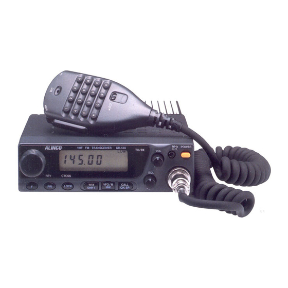
DR-130
CONTENTS
SPECIFICATIONS
1)
General
2)
Transmitter
3)
Receiver
CIRCUIT DESCRIPTION
1)
Receiver System
2)
Transmitter System
3)
PLL Circuit
4)
Terminal Function of Microprocessor
5)
Terminal Connection of Microprocessor
SEMICONDUCTOR DATA
1)
AK2341
2)
AN78LO5M
3)
AN8010M
4)
BU4052BF
5)
LR408721
6)
M5218FP
7)
M56760FP
8)
MC7808CT
9)
RH5VA32AA-T1
10) RH5VA45AA-T1
11) S-AV17
12) TK10487MTR
13) AT24CO2N-10SI-2.7
14) AT24CO8-10SI-2.7
15) uPC1241H
16)
Transistor, Diode and LED Outline Drawings
17) LCD Connection
EXPLODED VIEW
1)
Bottom View
2)
LCD View
3)
Top, Front View 1
4)
Top, Front View 2
VERSION TABLE
Service Manual
2
PARTS LAST
2
MAIN Unit
2
CPU Unit
VCO Unit
3
SP Unit
4
EJ19u.
4
Mechanical Parts
5 - 7
Others
8
Packing..
EJ20u
9
EMS-5A
10
EMS-11
10
ADJUSTMENT
10
1) Required Test Equipment.
11
2) Adjustment for DR-130
11
3) Adjustment Points
12
4) Adjustment Quick Reference
13
CIRCUIT DIAGRAM
13
1) EMS-5A
13
2) EMS-11
14
3) Main Unit (T/E/EZ/EA/TA)
15
4) Main Unit (TEl1/TE2)
15
5) CPU Unit
15
PC BOARD VIEW
16
1) Main Unit Side A
16
2) Main Unit Side B
17
3) CPU Unit Side A.
4) CPU Unit Side B
18
5) VCO Unit Side A
18
6) VCO Unit Side B
19
BLOCK DIAGRAM
20
21
ALINCO INCORPORATED
TWIN 21 M.I.D. TOWER BUILDING 23F, 1-61, 2-CHOME,
SHIROMI CHUO-KU , OSAKA, 540-8580 JAPAN
Tel (81)6-6946-8150 fax (81)6-6946-8175
e-mail: export@alinco.co.jp
22-23
24
25
25
25
25
25
25
26
26
26
27
28~29
30
30
31
31
32
33
34
35
36
37
37
38
38
39
Advertisement

Related Manuals for Alinco DR-130


Summary of Contents for Alinco DR-130
- Page 1 Packing.. SEMICONDUCTOR DATA EJ20u AK2341 EMS-5A AN78LO5M EMS-11 AN8010M ADJUSTMENT BU4052BF 1) Required Test Equipment. LR408721 2) Adjustment for DR-130 28~29 M5218FP 3) Adjustment Points M56760FP 4) Adjustment Quick Reference MC7808CT CIRCUIT DIAGRAM RH5VA32AA-T1 1) EMS-5A 10) RH5VA45AA-T1 2) EMS-11...
- Page 2 SPECIFICATIONS 1) General Frequency Coverage: RX: 136.000 ~ 174.000MHz (T version) TX: 144.000 ~ 148.000MHz (T version) RX: 144.000 ~ 146.000MHz (E/EZ version) TX: 144.000 ~ 146.000MHz (E/EZ version) RX: 130.000 ~ 174.000MHz (EA/TA version) TX: 130.000 ~ 174.000MHz (EA/TA version) RX: 136.000 ~ 155.000MHz (TE1 version) TX: 136.000 ~ 155.000MHz...
- Page 3 CIRCUIT DESCRTPTION 1) Receiver System 1. Front End The signal from the antenna is passed through a low-pass filter and input to the voltage step up circuit consisting Of L14. The signal from L14 is led to the gate of Q1. D19 is the diode limiter circuit against the excessive input power of more than 20dBm.
- Page 4 2) Transmitter System 1. Modulation Circuit 3) PLL Circuit The microphone amplifier IC1 (IDC, LPF) consists of two operational amplifi- ers. The signal from the microphone is led to pre-emphasis circuit consisting of C36 and R47 and then to the limiter circuit. The limiter circuit uses the saturation of the OP amplifier.
- Page 5 4) Terminal Function of Microprocessor Port No. I/O Logic PinName Description SEG19 LCDSegment19 Output SEG20 LCDSegment20 Output SEG21 LCDSegment21 Output SEG22 LCDSegment22 Output SEG23 LCDSegment23 Output AnalogGround 0V Vref Reference Voltage Input 5V CPU Power Supply hnput 5V 1750_ ToneBurstOutput 10 O Clock BEEP BeepToneOutput...
- Page 6 Port No. I/O Logic PinName Description 40 I/O Clock Data Output for EEPROM 41 O Clock Clock Output 42 O Clock DataOutput 43 O Clock Strobe Output for PLL IC 44 O Clock Strobe Output for CTCSS IC I Active Low SFT Shift Key Input I Active High SD Signal Detection Input...
- Page 7 Page-8...
- Page 8 Page-9...
- Page 9 Page-10...
- Page 10 Page-11...
- Page 11 Page-12...
- Page 12 Page-13...
- Page 13 Page-14...
- Page 14 Page-15...
- Page 15 Page-16...
- Page 16 Page-17...
- Page 18 ES0017 KZ0047AZ FM0152 FF0028 FF0031 KS0041B Page-19...
- Page 19 FF0030 FM0152 SS0052B FP0034 NK0009B NK0010A Page-20...
- Page 20 VERSION TABLE 1)CPU UNIT W3/W4 R284 R286 R296 R297 CN204 IC208 R294/R295 UE0165 - UE0165 - AT24CO8-10SI UE0165 - UE0165 - UE0165 - UE0165 - TX Free RX Free Tranking 12.5k/5k Tranking V/U 2) MAIN UNIT C71,7 4,75,7 C112 C139 C149 T/E/EZ/EA/TA 1000p 10u/16V...
- Page 26 ADJUSTMENT 11. Distortion Meter 1) Required Test Equipment 1. Digital Multimeter Measurable frequency 1kHz Voltage range: FS= 18V or so Input level: Up to 40dB Input resistance: 1M ohm or more Distortion level: 1% - l00% 2. Regulated Power Supply 12.
- Page 27 2) Adjustment for DR130 SSG Mod:1KHz +/-3.5KHz/DEV SP terminal is connected to 8ohm dummy load. RX speaker output level is 50 to 100mW 1. Power supply voltage is 13.8V. Power switch is off. 2. Turn the squelch and volume knobs counterclockwise. 3.
- Page 28 TX Adjustment Condition Measurement Adjustment Specification/ Item Test equipmen Unit Terminal Unit Parts Method Remarks VR1: max Power:High PTT: ON High Power Frequency:145.00MHz Power:High +/- 1.0W PTT: ON Power Meter Back Main Below 10.5A Frequency:130.00MHz Above 5W Power:High Check (T.E.EZ) PTT: ON Frequency:174.00MHz Above 5W...
- Page 29 3) Adjustment Points 4) Adjustment Quick Reference SSG Output = EMF Parts Item Specifications Specifications RX Sensitivity -10dBpV (12dB SINAD) -10dBpV (12dB SINAD) RX Sensitivity -10dBpV (12dB SINAD) -10dBpV (12dB SINAD) RX Sensitivity -10dBpV (12dB SINAD) -10dBpV (12dB SINAD) RX Sensitivity -10dBpV (12dB SINAD) -10dBpV (12dB SINAD) L302...
- Page 33 Page-34...
Need help?
Do you have a question about the DR-130 and is the answer not in the manual?
Questions and answers