Table of Contents
Advertisement
Quick Links
SERVICE MANUAL
Ver 1.0 2004.02
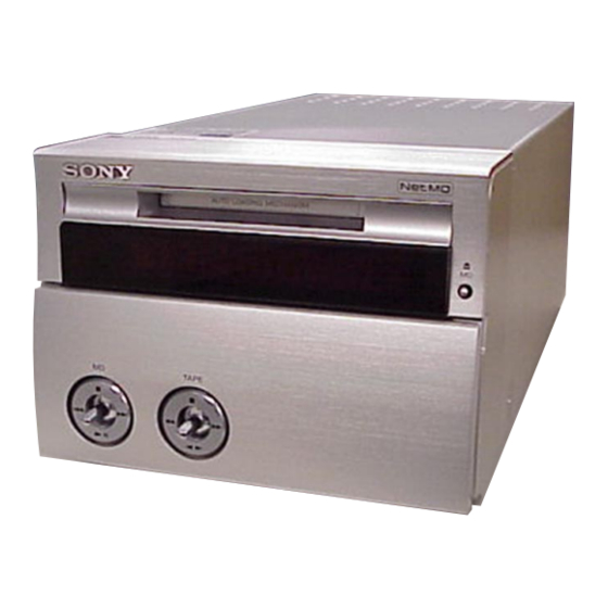
MDS-SE9 is MD deck and Tape deck
section in CMT-SE9.
MD deck section
System
Laser
Sampling frequency
Frequency response
Sony Corporation
9-961-479-01
2004B1678-1
Home Audio Company
© 2004.02
Published by Sony Engineering Corporation
Model Name Using Similar Mechanism
MD
MD Mechanism Type
Section
Optical Pick-up Type
Model Name Using Similar Mechanism
Tape deck
Section
Tape Transport Mechanism Type
SPECIFICATIONS
Tape deck section
Minidisc digital audio
Recording system
system
Frequency response
Semiconductor laser
(λ=780 nm)
Emission duration:
General
continuous
Power requirements
44.1 kHz
Power consumption
5 Hz – 20 kHz
Dimensions(w/h/d)
Mass
Design and specifications are subject to change
without notice.
MDS-SE9
4-track 2-channel stereo
50 – 13,000 Hz, using
Sony TYPE I cassettes
230 V AC, 50/60 Hz
13 W
Approx. 155 × 120 × 345 mm
Approx. 4.0 kg
MD/TAPE DECK
UK Model
HCD-CP505
MDM-7S2D
KMS-262E
NEW
CMAL2Z8
Advertisement
Table of Contents

Related Manuals for Sony MDS-SE9


Summary of Contents for Sony MDS-SE9
- Page 1 MDS-SE9 SERVICE MANUAL UK Model Ver 1.0 2004.02 MDS-SE9 is MD deck and Tape deck section in CMT-SE9. Model Name Using Similar Mechanism HCD-CP505 MD Mechanism Type MDM-7S2D Section Optical Pick-up Type KMS-262E Model Name Using Similar Mechanism Tape deck...
- Page 2 Note 1: MDS-SE9 does not operate independently. HCD-SE9 is required to operate this. In this case of a service, please connect HCD-SE9. Note 2: Incorrect operations may be performed if the test mode is not entered properly.
-
Page 3: Table Of Contents
MDS-SE9 TABLE OF CONTENTS 1. SERVICING NOTES 7. DIAGRAMS ····················································· 10 ······································································ 41 7-1. Block Diagrams – Main Section – ························································ 42 2. GENERAL ········································································ 13 – MD Section – ·························································· 43 – USB Section – ························································· 44 3. DISASSEMBLY ······························································... - Page 4 The sound source is a copy of a commercially refer to the following list. If any problem available music software or CD-R. persists, consult your nearest Sony dealer. cThe Serial Copy Management System prevents making a digital copy. In addition, you cannot copy from a CD-R.
- Page 5 MDS-SE9 Incomplete! Messages Adjustment of the recording level after recording or Fade-in and Fade-out procedures have failed since One of the following messages may appear or the system was either subject to vibration or there is flash in the display during operation.
- Page 6 MDS-SE9 Track End You have reached the end of the track while adjusting the dividing point during the Divide Function. Tr Protected Tracks and other data that have been checked out on Net MD equipment are protected, so you cannot use some of the MD editing functions.
- Page 7 MDS-SE9 Note 1: MDS-SE9 does not operate independently. HCD-SE9 is required to operate this. In this case of a service, please connect HCD-SE9. Note 2: Incorrect operations may be performed if the test mode is not entered properly. In this case, press the ?/1 button to turn the power off, and retry to enter the test mode.
- Page 8 MDS-SE9 Items of Error History Mode Items and Contents Display History op rec tm Displays the accumulated recording time. When the accumulated recording time is more than 1 minute, displays the hour and minute When less than 1 minute, displays “Under 1 min”...
- Page 9 MDS-SE9 Table of Error Codes Error Code Description Could not perform loading The changer error occurred Loading switches combined incorrectly Timed out without reading the top of PTOC Could read top of PTOC, but detected error Timed out without accessing UTOC...
-
Page 10: Servicing Notes
MDS-SE9 SECTION 1 SERVICING NOTE Service Position (Checking TC) Disassemble the MD mechanism deck and the MD DIGITAL board. Connect the wire (flat type, 25 cores) as shown in the figure to check the tape mechanism. MD mechanism deck (MDM-7S2D) Please put MD mechanism deck on a rest with an insulation sheet etc. - Page 11 MDS-SE9 Jig For Checking BD Board Waveform The special jig (J-2501-196-A) is useful for checking the waveform of the BD board. The names of terminals and the checking items to be performed are shown as follows. I+3V : For measuring Iop (Check the deterioration of the optical pick-up laser)
- Page 12 MDS-SE9 Iop DATA RECORDING AND DISPLAY WHEN OPTICAL PICK-UP AND NON-VOLATILE MEMORY (IC195 OF BD BOARD) ARE REPLACED The Iop value labeled on the optical pick-up can be stored in the non-volatile memory. By storing the value, it will eliminate the need to look at the value on the label of the optical pick-up.
-
Page 13: General
MDS-SE9 SECTION 2 GENERAL This section is extracted from instruction manual. Main unit BUTTON DESCRIPTIONS ALPHABETICAL ORDER x (stop) 46 N – Z A – M ./> (go back/go forward) NET MD 2 DIRECTION 8 REC 8 DISPLAY 3 NX (play/pause) 4... - Page 14 MDS-SE9 Remote control ALPHABETICAL ORDER BUTTON DESCRIPTIONS ?/1 (power) 1 A – F G – Z MD N (play) 5 ALBUM +/–* qd GROUP SKIP 7 PC N (play) 5 ANGLE* 8 MD GROUP 7 SA-CD/DVD N/SELECT (play) AUDIO* 8 MENU/NO 4 CLEAR w;...
-
Page 15: Disassembly
MDS-SE9 SECTION 3 DISASSEMBLY • The equipment can be removed using the following procedure. • The dotted square with arrow ( ) prompts you to move to the next job when all of the works within the dotted square ( ) are completed. -
Page 16: Top Cover
MDS-SE9 Note: Follow the disassembly procedure in the numerical order given. 3-1. TOP COVER 4 top cover 1 two screws (+BVTP 3 × 8) 3 case screw 2 case screw 3-2. FRONT PANEL SECTION 2 earth wire 7 claw 3 Peel off the himeron tape. -
Page 17: Panel Board
MDS-SE9 3-3. PANEL BOARD 2 wire (flat type) (13 core) (CN801) 1 eight screws (+BV 2.6 × 8) 3 PANEL board 3-4. POWER TRANSFORMER 4 power transformer 2 connector (CN51) 3 connector (CN2) 1 four screws (+BVTP 3 × 8) -
Page 18: Md Digital Board
MDS-SE9 3-5. MD DIGITAL BOARD 1 two screws (+BVTP 3 × 8) (CN501) 5 MD DIGITAL board 2 wire (flat type) (25 core) 3 connector (CN705) 4 connector (CN703) (CN704) 3-6. MD MECHANISM DECK (MDM-7S2D) 1 four step screws (+BVTTWH M3) -
Page 19: Holder Assy
MDS-SE9 3-7. HOLDER ASSY 3 holder assy 1 tension spring (holder) 2 hook 3-8. BD BOARD 1 Remove the two solderings. (sled motor) 2 Remove the two solderings. (spindle motor) M102 6 flexible board M101 (CN101) M103 3 Remove the two solderings. -
Page 20: Loarding Motor, Spindle Motor, Sled Motor
MDS-SE9 3-9. LOARDING MOTOR, SPINDLE MOTOR, SLED MOTOR 1 lever (head) 8 tapping screw 3 torsion spring (spindle) (M1.7 ) 2 belt (loading) 9 gear (sa) 4 two screws 0 two screws (PWH 1.7 × 3.5) (PWH 1.7 × 2.5) -
Page 21: Optical Pick-Up (Kms-262E)
MDS-SE9 3-11. OPTICAL PICK-UP (KMS-262E) 8 optical pick-up (KMS-262E) 6 main shaft 3 screw (+B (P) TRI 2 × 6 CZN) 7 flexible board 4 base (BU-A) 5 two screws (+KTP 2 × 6) 1 screw (+B (P) TRI 2 × 6 CZN) 2 base (BU-D) 3-12. -
Page 22: Main Board
MDS-SE9 3-13. MAIN BOARD qa MAIN board 6 three screws (+BV sumitite B3 3 × 8) q; connector (CN52) 2 two screws (+BVTP 3 × 8) 3 connector (CN431) 1 five screws (+BVTP 3 × 8) 8 connector (CN301) 7 connector... -
Page 23: Tape Mechanism Deck
MDS-SE9 3-15. TAPE MECHANISM DECK 1 four screws 5 tape mechanism deck (+BV sumitite B3 3 × 6) (CN321) 4 wire (flat type) (10 core) 2 connector 3 connector (CN201) (CN301) -
Page 24: Test Mode
SECTION 4 TEST MODE Note 1: MDS-SE9 does not operate independently. HCD-SE9 is required to operate this. In this case of a service, please connect HCD-SE9. Note 2: Incorrect operations may be performed if the test mode is not entered properly. - Page 25 MDS-SE9 5. Key Test Mode Procedure: Press the ?/1 button to turn on the power.(HCD-SE9) Press three bottons Z TAPE , TAPE X and TAPE x simultaneously, and be in the state of version test mode. Press [TAPE DIRECTION] button to select the key test mode.
- Page 26 MDS-SE9 Group Display Details Mark Check Service AUTO CHECK Automatic self-diagnosis Err Display Error history display, clear TEMP ADJUST Temperature compensation offset adjustment LDPWR ADJUST Laser power adjustment Iop Write Iop data writing Iop NV Save Writes current Iop value in read nonvolatile memory using microprocessor...
- Page 27 MDS-SE9 5-2. Operating the Continuous Recording Mode (Use only when performing self-recording/playback check) Entering the continuous recording mode (1) Set a recordable disc in the unit. (2) Press the MD . or MD > button to display “CREC 2MODE” (C37).
-
Page 28: Mechanical Adjustments
MDS-SE9 SECTION 5 SECTION 6 MECHANICAL ADJUSTMENTS ELECTRICAL ADJUSTMENTS PRECAUTION TAPE SECTION 0 dB=0.775V Clean the following parts with a denatured-alcohol-moistened swab: Demagnetize the record/playback head with a head demagne- record/playback head pinch roller tizer. erase head rubber belts Do not use a magnetized screwdriver for the adjustments. - Page 29 MDS-SE9 Mode: Playback Record Bias Adjustment Procedure : test tape 1. Press the [FUNCTION] button to select TAPE. (HCD-SE9) MD/TAPE OUT (J401) P-4-A100 2. Insert a tape into deck, press the [TAPE REC] button, and then (10kHz, –10dB) L-CH oscilloscope press the TAPE X button to start recording.
-
Page 30: Md Section
MDS-SE9 MD SECTION 1. Parts Replacement and Adjustment If malfunctions caused by optical pick-up such as sound skipping are suspected, follow the following check. Check before replacement Start 6-2. Laser Power Check (See page 33) 6-3. Iop Compare (See page 33) 6-4. - Page 31 MDS-SE9 Flow Chart for Adjustment Start After turning the power off and on, initialises the non-volatile IC195 replacement memory (EEPROM). 7. Initial setting of adjustment value (See page 36) OP or IC195 replacement IC101, IC195 or D101 9. Temperature compensation offset adjustment (See page 36)
- Page 32 MDS-SE9 Precautions for Checking Laser Diode 4. Precautions for Adjustments Emission 1. When replacing the following parts, perform the adjustments To check the emission of the laser diode during adjustments, never and checks with in the order shown in the following table.
- Page 33 MDS-SE9 Using the Continuously Recorded Disc Procedure: Set the laser power meter on the objective lens of the optical * This disc is used in focus bias adjustment and error rate check. pick-up. (When it cannot be set properly, press the TAPE m The following describes how to create a continuous recording button or TAPE M button to move the optical pick-up.)
- Page 34 MDS-SE9 6-4. Auto Check 6-6. Traverse Check This test mode performs CREC and CPLAY automatically for mainly checking the characteristics of the optical pick-up. To Note 1:Data will be erased during MO reading if a recorded disc is used in this adjustment.
- Page 35 MDS-SE9 9. Press the [ENTER/START] button to display “EFB = 6-7. Focus Bias Check Change the focus bias and check the focus tolerance amount. P”. Procedure: Then, the optical pick-up moves to the pit area automatically 1. Load the test disc (MDW-74/GA-1).
- Page 36 MDS-SE9 Initial Setting of Adjustment Value 5. When the [ENTER/START] button is pressed, “TEMP = SAVE” will be displayed and turned back to “TEMP ADJUST” Note: Mode which sets the adjustment results recorded in the non-volatile (C03) display then. memory to the initial setting value. However the results of the tempera-...
- Page 37 MDS-SE9 6. Press the MD or MD button so that the reading of save?”, press the [ENTER/ > After the display changes to “Iop = the laser power meter becomes the specified value, press the START] button. [ENTER/START] button to save it.
- Page 38 MDS-SE9 8. Press the MD or MD button so that the waveform of 19. Press the Z MD button and take out the check disc. > the oscilloscope becomes the specified value. Adjustment Location: BD board (see page 40) (When the MD...
- Page 39 MDS-SE9 14. Error Rate Check 16. Auto Gain Control Output Level Adjustment Be sure to perform this adjustment when the optical pick-up is 14-1. CD Error Rate Check replaced. Procedure: If the adjustment results becomes “Adjust NG!”, the optical pick- 1.
- Page 40 MDS-SE9 Adjustment and checking Loacation: — BD BOARD (Side A) — — BD BOARD (Side B) — CN102 CN103 IC195 IC933 IC201 IC701 CN101 CN105 IC101 D101 Note: If is useful to use the jig for checking the waveform. (Refer to Servicing Notes on page 11).
-
Page 41: Diagrams
MDS-SE9 SECTION 7 DIAGRAMS • Circuit Boards Location THIS NOTE IS COMMON FOR PRINTED WIRING • Signal path. : DIGITAL IN BOARDS AND SCHEMATIC DIAGRAMS. MD DIGITAL board : DIGITAL OUT (In addition to this, the necessary note is printed : PB (TAPE) in each block.) -
Page 42: Block Diagrams
MDS-SE9 7-1. BLOCK DIAGRAMS – MAIN SECTION – SECTION (Page 44) IC401 SELECTOR LOUT IC402 J401(1/2) SECTION BUFFER (Page 44) J401(2/2) MD/TAPE IN A MD/TAPE R-CH OUT B R-CH IC201 IC151 PB/REC EQ AMP SYSTEM CONTROLLER Q421 INVERTER B IN... -
Page 43: Md Section
MDS-SE9 – – MD SECTION IC201 DIGITAL SERVO DIGITAL SIGNAL PROC. DATAI IC181 DATAI Q181,182 LRCKI HR901 LRCKI OVER WRITE XBCKI OVER WRITE EFMO XBCKI HEAD DRIVE HEAD MCLK FS256 SECTION DOUT (Page 44) DOUT DIN1 DIN1 OPTICAL PICK-UP BLOCK... -
Page 44: Usb Section
MDS-SE9 – – USB SECTION IC701 AD/DA CONVERTER IC441 IC442 DIGITAL DIGITAL DIN-CD 44 RX2 OPTICAL OPTICAL DIGITAL IN DIGITAL OUT OPTICAL C OPTICAL D 42 RX1 LOUT MAIN LOUT SECTION ROUT R-CH MAIN (Page 42) SECTION (Page 42) 4 RX4... -
Page 45: Printed Wiring Board - Bd Board
MDS-SE9 7-2. PRINTED WIRING BOARD – BD BOARD – • : Uses unleaded solder. • See page 41 for Circuit Boards Location. MD DIGITAL MD DIGITAL BOARD BOARD CN701 CN702 (Page 52) (Page 52) IC181 IC803 IC933 IC201 (REC) IC926... -
Page 46: Schematic Diagram - Bd Board (1/2)
MDS-SE9 7-3. SCHEMATIC DIAGRAM – BD BOARD (1/2) – (1/2) R707 4.7k C704 0.047 R712 TP701 Q704 L701 2SA1576A-T106 R703 R705 IC701 4.7k TLV2361CDBV R710 R713 COMPARATOR C702 R706 2.2k R709 Q702 2.2k FMW1-T-148 R704 L202 Q701-704 R702 C703 R708... -
Page 47: Schematic Diagram - Bd Board (2/2)
MDS-SE9 7-4. SCHEMATIC DIAGRAM – BD BOARD (2/2) – IC195 is a written in and settled EEPROM. Supply with a single article has not been carried out. In case you exchange by BD board (A-4731-095-A), please put on IC195 currently used with the model again. -
Page 48: Printed Wiring Board - Main Board (Side A)
MDS-SE9 7-5. PRINTED WIRING BOARD – MAIN BOARD (SIDE A) – • : Uses unleaded solder. • See page 41 for Circuit Boards Location. -
Page 49: Printed Wiring Board - Main Board (Side B)
MDS-SE9 7-6. PRINTED WIRING BOARD – MAIN BOARD (SIDE B) – • : Uses unleaded solder. • See page 41 for Circuit Boards Location. MD DIGITAL MD DIGITAL BOARD BOARD CN703 CN705 TAPE (Page 52) (Page 52) MECHANISM DECK(1/2) (FOR FLASH WRITER) -
Page 50: Schematic Diagram - Main Board (1/2)
MDS-SE9 7-7. SCHEMATIC DIAGRAM – MAIN BOARD (1/2) – J401 CN301 CN431 CN321 Q324 IC301 2SB1116A-TP-LK BA6956AN D432 UDZSTE-176.2B R321 R328 R323 2.2k FB431 D433 IC442 D431 TOTX179L UDZSTE-176.2B 1SS355TE-17 C444 TP321 R401 R451 R329 FB432 Q322 2.2k 2SB1068TP-K Q431... -
Page 51: Schematic Diagram - Main Board (2/2)
MDS-SE9 7-8. SCHEMATIC DIAGRAM – MAIN BOARD (2/2) – • See page 61 for IC Pin Function Description. R159 4.7k IC202 BA3126N CN151 C267 R263 R264 C266 R265 6.8k 470p 2.2k X151 C264 C268 R266 R267 6.8k C262 0.01 C265... -
Page 52: Printed Wiring Board - Md Digital Board
MDS-SE9 7-9. PRINTED WIRING BOARD – MD DIGITAL BOARD – • : Uses unleaded solder. • See page 41 for Circuit Boards Location. MAIN BOARD POWER CN502 BOARD (Page 49) CN91 (Page 56) R1018 R1020 R1019 • Semiconductor Location BOARD... -
Page 53: Schematic Diagram - Md Digital Board
MDS-SE9 7-10. SCHEMATIC DIAGRAM – MD DIGITAL BOARD – • See page 62, 63 for IC Pin Function Description. C716 CN705 R1018 100 FB705 FL-CLK R1019 100 FL-DATA R712 FB704 C714 FL-CS C713 IC722 R1020 100 6.3V TC7WH00FK MAIN (TE85R) -
Page 54: Printed Wiring Board - Panel Board
MDS-SE9 7-11. PRINTED WIRING BOARD – PANEL BOARD – • : Uses unleaded solder. • See page 41 for Circuit Boards Location. IC 851 MAIN BOARD CN181 (Page 49) NET MD DISPLAY TAPE SYNC REC ENTER/START MODE REC/REC IT REC MODE... -
Page 55: Schematic Diagram - Panel Board
MDS-SE9 7-12. SCHEMATIC DIAGRAM – PANEL BOARD – FL851 C860 220p R858 C861 220p R857 Q851 2SC3052F-T1-LF R860 Q852 2SC3052F-T1-LF R859 R851 R852 R853 R854 C855 C856 (Page 51) R801 R802 R803 2.2k 2.2k CN801 IC851 MSM9202-07G4-KDR1 S801 S802 S803... -
Page 56: Printed Wiring Board - Power Board
MDS-SE9 7-13. PRINTED WIRING BOARD – POWER BOARD – • : Uses unleaded solder. • See page 41 for Circuit Boards Location. MAIN BOARD CN101 (Page 49) T101 MD DIGITAL POWER BOARD TRANSFORMER CN704 (Page 52) • Semiconductor Location Ref. No. Location... -
Page 57: Schematic Diagram - Power Board
MDS-SE9 7-14. SCHEMATIC DIAGRAM – POWER BOARD – AC OUTLET 1SS355TE-17 T1AL/250V CN51 R76 R77 1/4W 10EDB40-TB3 1SS355TE-17 UDZSTE-1730B 1SS355TE-17 10EDB40-TB3 10EDB40-TB3 CN91 2.2k 1/2W 0.01 10EDB40-TB3 2SB798-T1DK 1/2W D3SBA20-4101 (Page 53) 10000 1SS355TE-17 1.8k 1SS355TE-17 1SS355TE-17 (Page 50) EPT51... - Page 58 MDS-SE9 • IC BLOCK DIAGRAMS – BD Board – IC201 CXD2664R IC401 BH6519FS-E2 114 113 112 110 109 108 107 106 105 104 103 102 101 100 99 98 97 93 92 INTERFACE INTERFACE DCHG AVS2 CHARGE PREDRIVE PREDRIVE AVD2 SPINDLE PUMP.
- Page 59 MDS-SE9 – MD DIGITAL Board – IC701 AK4584VQ TEST2 33 ROUT LOUT A_LRCK D_LRCK A_BICK D_BICK DATT DATT IPGA A_DATA D_DATA VCOM SMUTE A_MCLK D_MCLK S_LRCK AUDIO S_BICK INTERFACE S_DATAI 29 M/S S_DATAO R_LRCK T_LRCK INT0 LRCK R_BICK T_BICK R_DATA...
- Page 60 MDS-SE9 IC705 CXD1875TQ CPU_SO XTAL CPU_SI EXTAL VSC3 VDEA1 CPU_XCS VDC1 VDC2 DNK_RS CPU_INT DNK_ST CONTROL PLLSW DNK_SI VDEC0 DNK_SO RESET DNK_CS DNK_CK VSC4 VSC1 TEST2 EXT_IF3 TEST3 AUDIO IC721 M62016FP-E1 IC781 LB1830M-S-TE-L VREF VCONT VREF INTERRUPT SIGNAL – GENERATOR...
-
Page 61: Ic Pin Function Description
MDS-SE9 7-15. IC PIN FUNCTION DESCRIPTION • IC151 M38514M6-C12FP SYSTEM CONTROLLER (MAIN Board) Pin No. Pin Name Description – Power supply terminal VREF – Reference voltage input terminal AVSS – Ground terminal (analog) 4052A Selection signal input to the selector (IC401) - Page 62 MDS-SE9 • IC702 M3062VMWP-A18GP MD MASTER CONTROLLER (MD DIGITAL Board) Pin No. Pin Name Description – Power supply terminal VREF – Reference voltage input terminal AVSS – Ground terminal (analog) 4052A Selection signal input to the selector (IC401) 4052B Selection signal input to the selector (IC401) P.DOWN...
- Page 63 MDS-SE9 • IC703 MB89051PFM-101-BNDE1 USB I/F (MD DIGITAL Board) Pin No. Pin Name Description Clock input from the MD Master Controller (IC702) VBUSDET VBUS check signal input MDCS Chip selection signal from the MD Master Controller (IC702) 4, 5 Not used (open)
-
Page 64: Exploded Views
MDS-SE9 SECTION 8 EXPLODED VIEWS NOTE: • -XX, -X mean standardized parts, so they may • The mechanical parts with no reference The components identified by mark 0 or have some differences from the original one. number in the exploded views are not supplied. -
Page 65: Front Panel Section
4-245-464-01 DAMPER 1-769-972-11 WIRE (FLAT TYPE) (13 CORE) X-4955-754-1 LID (MD) ASSY 4-931-757-31 SCREW(DIA.2.6X8)(IT3B),TAPPING 4-245-354-01 WINDOW (FL) A-4732-544-A PANEL BOARD, COMPLETE 4-969-961-11 EMBLEM (NO.4), SONY 4-245-356-01 KNOB (LEVER) 4-247-906-01 BRACKET(B0) 4-232-478-31 FOOT 4-247-905-01 PLATE (ALUMINUM PANEL), GROUND 4-245-372-01 BRACKET (LID) -
Page 66: Chassis Section
MDS-SE9 8-3. CHASSIS SECTION supplied supplied supplied F101 supplied T101 supplied Ref. No. Part No. Description Remarks Ref. No. Part No. Description Remarks A-4732-542-A MAIN BOARD, COMPLETE A-4732-549-A POWER BOARD, COMPLETE 1-796-665-11 DECK, MECH 4-232-478-31 FOOT 1-827-281-11 WIRE (FLAT TYPE) (10 CORE) -
Page 67: Md Mechanism Deck Section-1 (Mdm-7S2D)
MDS-SE9 8-4. MD MECHANISM DECK SECTION-1 (MDM-7S2D) supplied supplied not supplied MD mechanism deck section-2 (MDM-7S2D) Ref. No. Part No. Description Remarks Ref. No. Part No. Description Remarks * 151 4-996-267-01 BASE (BU-D) A-4680-638-B RETAINER COMPLETE ASSY 4-231-319-01 SCREW (2X6) CZN, +B (P) TRI... -
Page 68: Md Mechanism Deck Section-2 (Mdm-7S2D)
MDS-SE9 8-5. MD MECHANISM DECK SECTION-2 (MDM-7S2D) HR901 S102 M101 M102 M103 Ref. No. Part No. Description Remarks Ref. No. Part No. Description Remarks 4-231-319-01 SCREW (2X6) CZN, +B (P) TRI 4-227-004-01 GEAR (LC) 3-372-761-01 SCREW (M1.7), TAPPING 4-227-005-01 GEAR (LD) -
Page 69: Electrical Parts List
MDS-SE9 SECTION 9 ELECTRICAL PARTS LIST NOTE: • Due to standardization, replacements in the • COILS When indicating parts by reference number, parts list may be different from the parts uH: µH please include the board name. specified in the diagrams or the components •... - Page 70 MDS-SE9 Ref. No. Part No. Description Remarks Ref. No. Part No. Description Remarks CN102 1-784-835-21 CONNECTOR, FFC (LIF (NON-ZIF)) 27P R106 1-216-845-11 METAL CHIP 100K 1/16W CN103 1-784-869-41 CONNECTOR, FFC (LIF (NON-ZIF)) 17P R107 1-216-819-11 METAL CHIP 1/16W * CN104...
- Page 71 MDS-SE9 MAIN Ref. No. Part No. Description Remarks Ref. No. Part No. Description Remarks R710 1-218-887-11 METAL CHIP 0.5% 1/10W C243 1-162-961-11 CERAMIC CHIP 330PF R711 1-216-833-11 METAL CHIP 1/16W C244 1-162-928-11 CERAMIC CHIP 120PF R712 1-216-809-11 METAL CHIP 1/16W...
- Page 72 MDS-SE9 MAIN Ref. No. Part No. Description Remarks Ref. No. Part No. Description Remarks C504 1-162-964-11 CERAMIC CHIP 0.001uF IC301 8-759-598-69 IC BA6956AN C505 1-128-057-11 ELECT 330uF 20.00% 6.3V IC401 8-759-385-76 IC MC14052 BDR2 C506 1-162-964-11 CERAMIC CHIP 0.001uF IC402...
- Page 73 MDS-SE9 MAIN Ref. No. Part No. Description Remarks Ref. No. Part No. Description Remarks R159 1-216-829-11 METAL CHIP 4.7K 1/16W R301 1-216-821-11 METAL CHIP 1/16W R160 1-216-809-11 METAL CHIP 1/16W R161 1-216-809-11 METAL CHIP 1/16W R302 1-216-827-11 METAL CHIP 3.3K...
- Page 74 MDS-SE9 MAIN Ref. No. Part No. Description Remarks Ref. No. Part No. Description Remarks RV291 1-241-768-11 RES, ADJ, CARBON 220K C759 1-164-360-11 CERAMIC CHIP 0.1uF RV321 1-241-761-11 RES, ADJ, CARBON 1K C762 1-164-360-11 CERAMIC CHIP 0.1uF C763 1-164-360-11 CERAMIC CHIP 0.1uF...
- Page 75 MDS-SE9 PANEL Ref. No. Part No. Description Remarks Ref. No. Part No. Description Remarks < LINE FILTER > R769 1-216-835-11 METAL CHIP 1/16W R770 1-216-835-11 METAL CHIP 1/16W LF781 1-419-521-21 INDUCTOR R771 1-216-833-11 METAL CHIP 1/16W < TRANSISTOR > R772...
- Page 76 MDS-SE9 PANEL POWER Ref. No. Part No. Description Remarks Ref. No. Part No. Description Remarks C867 1-162-960-11 CERAMIC CHIP 220PF S815 1-762-875-21 SWITCH, KEYBOARD (REC (TAPE)) C868 1-162-960-11 CERAMIC CHIP 220PF S816 1-762-875-21 SWITCH, KEYBOARD (MODE (SYNC REC)) C869 1-162-960-11 CERAMIC CHIP...
- Page 77 MDS-SE9 POWER Ref. No. Part No. Description Remarks < LINE FILTER > 0 LF1 1-419-625-11 COIL, LINE FILTER < TRANSISTOR > 8-729-101-07 TRANSISTOR 2SB798-T1DK < RESISTOR > 1-216-817-11 METAL CHIP 1/16W 1-216-817-11 METAL CHIP 1/16W 1-216-824-11 METAL CHIP 1.8K 1/16W...
Need help?
Do you have a question about the MDS-SE9 and is the answer not in the manual?
Questions and answers