Table of Contents
Advertisement
Quick Links
SERVICE MANUAL
Compact disc player
Laser
Inputs/Outputs (i.LINK S200)
i.LINK connector
General
Power requirements
Power consumption
Dimensions (approx.) (w/h/d)
Mass (approx.)
SPECIFICATIONS
Semiconductor laser (λ = 800 nm)
Emission duration: continuous
4 pins - 4 pins (S200)
230 V AC, 50/60 Hz
22 W
430 × 70 × 315 mm
incl. projecting parts
4.6 kg
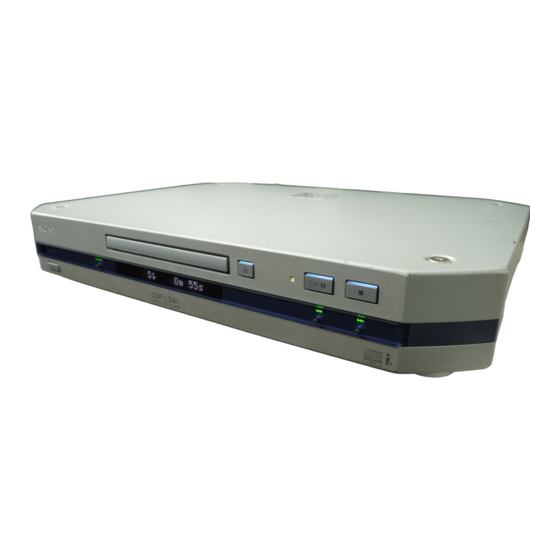
CDP-LSA1
Model Name Using Similar Mechanism
CD Mechanism Type
Base Unit Type
Optical Assy
Supplied accessories
i.LINK connecting calbe (4 pins - 4 pins) (1)
Remote commander (remote) (1)
Design and specifications are subject to change without
notice.
COMPACT DISC PLAYER
AEP Model
UK Model
NEW
CDM55B-21BD53A
BU-21BD53A
A-MAX.2
1
Advertisement
Table of Contents

Related Manuals for Sony CDP-LSA1


Summary of Contents for Sony CDP-LSA1
- Page 1 CDP-LSA1 SERVICE MANUAL AEP Model UK Model Model Name Using Similar Mechanism CD Mechanism Type CDM55B-21BD53A Base Unit Type BU-21BD53A Optical Assy A-MAX.2 SPECIFICATIONS Compact disc player Supplied accessories Laser Semiconductor laser (λ = 800 nm) i.LINK connecting calbe (4 pins - 4 pins) (1)
-
Page 2: Table Of Contents
TABLE OF CONTENTS 1. SERVICING NOTES ............3 2. GENERAL ................5 3. DISASSEMBLY 3-1. Case (Top) ................9 3-2. CD Mechanism Deck ............10 3-3. Base (Front) Assy, Panel ............. 10 3-4. Sub Main Board and Main Board ........11 3-5. -
Page 3: Servicing Notes
COMPONENTS IDENTIFIED BY MARK 0 OR DOTTED LINE WITH MARK 0 ON THE SCHEMATIC DIAGRAMS AND IN THE PARTS LIST ARE CRITICAL TO SAFE OPERATION. REPLACE THESE COMPONENTS WITH SONY PARTS WHOSE PART NUMBERS APPEAR AS SHOWN IN THIS MANUAL OR IN SUPPLEMENTS PUBLISHED BY SONY. - Page 4 • AFTER REPAIRING THE UNIT, PERFORM THE FOLLOWING STEPS BEFORE RETURNING TO CUSTOMER. Open tray. While pressing the DISPLAY button, press the Z button, the x button, and the . button in that order. Check to make sure that the STANDBY indicator lights up and remove the AC cord from its socket. Insert cushion in tray and close tray manually.
-
Page 5: General
SECTION 2 This section is extracted from instruction manual. GENERAL Remote sensor STANDBY indicator DISPLAY button and indicator A button PLAY/PAUSE indicator 7 button x button > button and indicator . button and indicator H.A.T.S. indicator +/1 button... -
Page 9: Disassembly
SECTION 3 DISASSEMBLY Note : Follow the disassembly procedure in the numerical order given. Case (Top) CD Mechanism Deck Tray, Gear And Cam Base Unit-1 (Page 10) (Page 12) (Page 12) Base (Front) Assy, Panel (Page 10) Base Unit-2 (BU-21BD53A) Optical pick-up Section (CD) (Page 13) (Page 13) -
Page 10: Cd Mechanism Deck
3-2. CD MECHANISM DECK 5 CD mechanism deck 3 screw (BVTT 3x6) Note : Be careful not to damage the surface of the tray in the case of the installation and the removal. two claws 1 flat type wire (31 core) (CN520) 2 connector (CN650) 3-3. -
Page 11: Sub Main Board And Main Board
3-4. SUB MAIN BOARD AND MAIN BOARD 2 SUB MAIN board 3 connector (CNP701) 6 two screws (BVTP 3x8) 5 two screws (BVTP 3x8) 8 MAIN board 1 connector (CN992) 4 two screws (BVTT 2.6x6) 3-5. TRANS BOARD 4 four screws 1 connector (BVTT 3x6) (CN752) -
Page 12: Tray, Gear And Cam
3-6. TRAY, GEAR AND CAM 4 belt (CDM55) 5 spacer (55) 6 pulley (LDG) 8 gear (B) 9 gear (A) 7 roller 0 cam (CDM55) 2 Push the claw in tne direction of arrow C. 1 Pull out the tray in the arrow direction A, and release the lock while pressing this claw in the arrow direction B. -
Page 13: Base Unit-2 (Bu-21Bd53A)
3-8. BASE UNIT-2 (BU-21BD53A) 2 three floating screws (DIA. 12) 1 floating screw (PTPWH M2.6) 3 base unit (BU-21BD53A) 4 spring, cone coil 4 spring, cone coil holder (BU) assy 3-9. OPTICAL PICK-UP SECTION (CD) 4 optical pick-up (CD) 1 flat type wire (14 core) (CN102) 3 sled shaft 2 Release the lever in the... -
Page 14: Bd Board
3-10. BD BOARD 6 BD board 1 flat type wire (14 core) (CN102) 4 Remove the two solders. sled motor 3 screw (BTP 2.6x6) 2 flat type wire (31 core) (CN101) spindle motor 5 Remove the two solders. -
Page 15: Test Mode
SECTION 4 TEST MODE Note that in order to enter test mode, it is first necessary to turn off test mode disabling. 4-1. How to release from test mode prohibition 1. While pressing the DISPLAY button, press the A button. 2. - Page 16 4-3. CD TEST MODE 1. While pressing the DISPLAY button, press the x button. 2. First release the x button press and then release the DISPLAY button. The following menu is displayed in CD TEST MODE. The . and > buttons may be used to make selections from this menu. The DISPLAY button is used to confirm menu selections and to enter test mode.
- Page 17 MODE DISPLAY DESCRIPTION Display after execution Note A>TRK ON Tracking servo on/off for E-F Switches each time DISPLAY balance button is pressed. TRK ON y TRK OFF B>SJI Used for E-F balance and S- Press DISPLAY button to begin. character checking. Press DISPLAY button again to end.
- Page 18 4-4. i.LINK TEST MODE DISPLAY “0”, “1”, and “2” will be displayed each time the DISPLAY button is pressed and the command will then be executed. Note DISPLAY 1 DISPLAY 2 Description DISPLAY 0 <[BACK]> The display mode will change every time D>i.LINK check the DISPLAY button is pressed.
- Page 19 DISPLAY 0 DISPLAY 1 DISPLAY 2 Description Note LINK IC [44] 0044 zzzzzzzz FUNCTION LINK IC Register [44] LINK IC [48] 0048 zzzzzzzz FUNCTION LINK IC Register [48] LINK IC [4C] 004C zzzzzzzz FUNCTION LINK IC Register [4C] LINK IC [50] 0050 zzzzzzzz FUNCTION LINK IC Register [50]...
- Page 20 26 Not linear PCM Sony DVs are designed to allow the use of 63 channels. MDs also have the same design, and it is impossible to use the same channel after it has already been used (i.e., the same...
-
Page 21: Electrical Adjustments
SECTION 5 ELECTRICAL ADJUSTMENTS Note : Note: Clear RF signal waveform means that the shape “◊” can be 1. CD Block is basically designed to operate without adjustment. clearly distinguished at the center of the waveform. Therefore, check each item in order given. RF signal waveform 2. - Page 22 Adjustment Location : [ BD BOARD ] — SIDE B — TP(VC) TP(FE) TP(TE) TP(RFAC) TP(XPCK) IC103...
-
Page 23: Diagrams
CDP-LSA1 SECTION 6 DIAGRAMS 6-1. CIRCUIT BOARDS LOCATION THIS NOTE IS COMMON FOR PRINTED WIRING • Indication of transistor BOARDS AND SCHEMATIC DIAGRAMS. (In addition to this, the necessary note is printed in each block.) These are omitted. For schematic diagrams. -
Page 24: Bd Section
CDP-LSA1 6-2. BLOCK DIAGRAMS – BD SECTION – SWITCH IC102 OPTICAL ASSY (A-MAX.2) A+5V DETECTOR IC101 IC103 DIGITAL SERVO D+5V RF AMP DIGITAL SIGNAL PRCESSOR ERROR DIGITAL D OUT IC104 CORRECTOR INV. RFAC PCM-D RF AC RF EQ REGISTER ADATA... -
Page 25: Main Section
CDP-LSA1 – MAIN SECTION – X502 24.576MHz IC503 IC504(1/3) C2P0 C2P0 AUDIO LINK TB2N IC530 D0-3 DATA0-3 CN571 TB2P DATA1 ADATA i.LINK TR/RE TA2N LINK BCK1 IC522 BCLK TA2P BUFFER LRCK1 LINK CONTROL LRCK UNIT CTL1 CTL1 TB0N CN570 CTL0... -
Page 26: Printed Wiring Board - Bd Section
CDP-LSA1 6-3. PRINTED WIRING BOARD – BD SECTION – • See page 23 for Circuit Board Location. • Semiconductor Location Ref. No. Location • Semiconductor IC101 Location IC102 IC103 Ref. No. Location IC171 IC191 IC104 There are a few cases that the part isn't mounted... -
Page 27: Schematic Diagram - Bd Section
CDP-LSA1 6-4. SCHEMATIC DIAGRAM – BD SECTION – • See page 33 for Waveforms. • See page 40 for IC Block Diagrams. • See page 41 for IC Pin Functions. FUNCTION OPTICAL ASSY (A-MAX.2) -
Page 28: Printed Wiring Board - Main (Side A) Section
CDP-LSA1 6-5. PRINTED WIRING BOARD – MAIN (SIDE A) SECTION – • See page 23 for Circuit Board Location. i.LINK S200 • Semiconductor Location Ref. No. Location Ref. No. Location Ref. No. Location D590 IC501 IC530 D591 IC503 D592 IC504... -
Page 29: Printed Wiring Board - Main (Side B) Section
CDP-LSA1 6-6. PRINTED WIRING BOARD – MAIN (SIDE B) SECTION – • See page 23 for Circuit Board Location. • Semiconductor Location Ref. No. Location Ref. No. Location Ref. No. Location D701 IC502 Q582 D704 IC650 Q583 Q602 D705 IC701... -
Page 30: Schematic Diagram - Main (1/3) Section
CDP-LSA1 6-7. SCHEMATIC DIAGRAM – MAIN (1/3) SECTION – • See page 28 for Printed Wiring Board. -
Page 31: Schematic Diagram - Main (2/3) Section
CDP-LSA1 6-8. SCHEMATIC DIAGRAM – MAIN (2/3) SECTION – • See page 28 for Printed Wiring Board. This is a written EEPROM. Not supplied in independently but is supplied as the MAIN BOARD, COMPLETE. FUNCTION... -
Page 32: Schematic Diagram - Main (3/3) Section
CDP-LSA1 6-9. SCHEMATIC DIAGRAM – MAIN (3/3) SECTION – • See page 28 for Printed Wiring Board. i.LINK S200 FUNCTION FUNCTION... - Page 33 CDP-LSA1 • WAVEFORMS – BD Board – – MAIN Board – – PANEL Board – IC901 tl (OSCI) IC101 t; (RFAC) IC501 qd (XOUT) 3.3Vp-p 3.3Vp-p 1.2Vp-p 10 MHz 2.23 MHz IC101 rd (RFDC) IC503 ed (XI) 3.2Vp-p 1.0Vp-p 24.576 MHz...
-
Page 34: Printed Wiring Board - Panel Section
CDP-LSA1 6-10. PRINTED WIRING BOARD – PANEL SECTION – • See page 23 for Circuit Board Location. • Semiconductor Location Ref. No. Location D901 D902 D903 D904 B-13 D905 D906 D908 D911 B-10 D912 B-11 IC901 A-12 IC902 B-13 There are a few cases that the part isn't mounted... -
Page 35: Schematic Diagram - Panel Section
CDP-LSA1 6-11. SCHEMATIC DIAGRAM – PANEL SECTION – • See page 33 for Waveforms. -
Page 36: Printed Wiring Board - Power Section
CDP-LSA1 6-12. PRINTED WIRING BOARD – POWER SECTION – • See page 23 for Circuit Board Location. There are a few cases that the part isn't mounted in model is printed on diagram. -
Page 37: Schematic Diagram - Power Section
CDP-LSA1 6-13. SCHEMATIC DIAGRAM – POWER SECTION –... -
Page 38: Printed Wiring Board - Flexible Section
CDP-LSA1 6-14. PRINTED WIRING BOARD – FLEXIBLE SECTION – • See page 23 for Circuit Board Location. OPTICAL ASSY (A-MAX.2) FLEXIBLE BOARD (Not supplied) (PAGE 26) FOCUS COIL TRACKING COIL There are a few cases that the part isn't mounted... -
Page 39: Printed Wiring Board - Loading Section
6-15. PRINTED WIRING BOARD – LOADING SECTION – • See page 23 for Circuit Board Location. (Page 29) (OPEN/CLOSE SW) There are a few cases that the part isn't mounted in model is printed on diagram. 6-16. SCHEMATIC DIAGRAM – LOADING SECTION – OPEN/CLOSE SWITCH CLOSE... - Page 40 6-17. IC PIN FUNCTIONS IC103 CXA2581N (BD BOARD) OFST RW/ROM RFDCI DVCC 11 RFDCO EQ IN 26 RFC 25 VFC 24 BST AC SUM ON/OFF 23 RFG VOFST 22 VCC RW/ROM VOFST RW/ROM RW/ROM 19 TE_BAL RW/ROM DVCC 18 TE APC-OFF(Hi-Z) RW/ROM SW 12...
- Page 41 6-18. IC PIN FUNCTIONS • IC101 CXD3008Q DIGITAL SIGNAL PROCESSOR (BD BOARD) Pin No. Pin Name Function DVDD0 — Digital power supply XRST System reset MUTE Muting selection pin DATA Serial data input, supplied from CPU XLAT Latch input, supplied from CPU CLOK Serial data transfer clock input, supplied from CPU SENS...
- Page 42 Pin No. Pin Name Function Tracking error signal input Center servo analog input RFDC RF signal input ADI0 Test pin (Not used) AVSS0 — Analog ground IGEN Power supply pin operational amplifiers AVDD — Analog power supply ASYO EFM full swing output ASYI Asymmetry comparate voltage input RFAC...
- Page 43 • IC501 M30624FGLFP-301FP1 SYSTEM CONTROL (MAIN BOARD) Pin. No. Pin Name Function FLDATA Serial data signal output to the display driver. FLCLK Serial clock signal output to the display driver. FLRESET Reset signal output to the display driver. FLLAT Serial latch signal output to the display driver. Not used.
- Page 44 Pin. No. Pin Name Function — Ground. 65 to 72 A7 to A0 Address bus signal output for IEEE1394. 73 to 88 D15 to D0 Data bus signal output for IEEE1394. RESET(1394) Reset signal output for IEEE1394. KEY1 Key input. KEY0 Key input.
- Page 45 • IC530 CXD3202AR AUDIO LINK (MAIN BOARD) Pin. No. Pin Name Function — Ground. 512FSI 512 fs input (used for flow control and ATRAC reception) (Conected to ground.) — Ground. XREQO/I ATRAC data request (Output for transmission, input for reception) (Pull up R) ADTI ATRAC transmission data input (Conected to ground.) XLATI...
- Page 46 Pin. No. Pin Name Function — Ground. XINT Interrupt signal transmitted to host. (Not used.) Chip select signal from host Write signal from host Read signal from host Address latch signal from host (enabled for M16); Fixed at "H" for Intel XRDY Ready signal transmitted to host (L = Ready) —...
- Page 47 Pin. No. Pin Name Function XCAS/TS20 DRAM XCAS. (Not used.) XOE/TS19 DRAM XOE. (Not used.) DRAM XWE. (Not used.) — Ground. 127 to 134 DT15 to 8 DRAM data bit 15 to 8. (Not used.) — Power supply. 136 to 143 DT7 to 0 DRAM data bit 7 to 0.
- Page 48 • IC503 CXD1945R PHY, I LINK I/F (MAIN BOARD) Pin. No. Pin Name Function Connected to ground. Connected to ground. DVSS — Ground. DVSS — Ground. Link power status. Indicates whether link power is off or on. L: OFF H: ON LREQ Link request.
- Page 49 Pin. No. Pin Name Function Arbitration / strobe output; arbitration / speed signal / data input. Reverse-phase I/O pins.(Not used) TA1P TBON Arbitration / speed signal / data output; arbitration / strobe input. Reverse-phase I/O pins. TB0P Arbitration / speed signal / data output; arbitration / strobe input. Reverse-phase I/O pins. TA0N Arbitration / speed signal / data output;...
-
Page 50: Exploded View
SECTION 7 EXPLODED VIEWS NOTE: • -XX, -X mean standardized parts, so they may The components identified by mark 0 or dotted line with mark 0 are critical for safety. have some differences from the original one. Replace only with part number specified. •... -
Page 51: Chassis Section
7-2. CHASSIS SECTION CDM55B-21BD53A T751 not supplied The components identified by mark 0 or dotted line with mark 0 are critical for safety. Replace only with part number specified. Ref. No. Part No. Description Remarks Ref. No. Part No. Description Remarks 4-225-902-01 PANEL,BACK 4-225-913-01 PANEL, LOADING... -
Page 52: Cd Mechanism Deck (Cdm55B-21Bd53A)
7-3. MECHANISM SECTION-1 (CDM55B-21BD53A) not supplied not supplied BU-21BD53A M103 Ref. No. Part No. Description Remarks Ref. No. Part No. Description Remarks 4-985-672-01 SCREW (+PTPWHM 2.6), FLOATING 4-925-315-31 DAMPER 4-220-230-01 CHASSIS 4-226-180-01 TRAY (55-L) 1-674-336-12 LOADING BOARD 4-220-951-02 SHEET (KH) 4-220-229-01 LEVER (SW) 4-230-386-01 INSULATOR (BU21) 4-220-239-01 SPRING, TORSION... -
Page 53: Base Unit (Bu-21Bd53A)
7-4. MECHANISM SECTION-2 (BU-21BD53A) not supplied not supplied not supplied not supplied not supplied Ref. No. Part No. Description Remarks Ref. No. Part No. Description Remarks A-4725-106-A BD BOARD, COMPLETE 1-792-396-11 WIRE, (FLAT TYPE) (31 CORE) A-4677-299-A BASE UNIT (BU-21BD53A) 3-317-552-71 SCREW (M1.7) A-4735-001-A PULLEY ASSY, DISC A-4735-000-A CAP ASSY, CENTERING... -
Page 54: Electrical Parts List
SECTION 8 ELECTRICAL PARTS LIST NOTE: Ref. No. Part No. Description Remarks Ref. No. Part No. Description Remarks • Due to standardization, replacements in the • COILS When indicating parts by reference number, parts list may be different from the parts uH: µH please include the board name. - Page 55 FLEXIBLE LOADING MAIN Ref. No. Part No. Description Remarks Ref. No. Part No. Description Remarks R127 1-216-033-00 METAL CHIP 1/10W 1-115-339-11 CERAMIC CHIP 0.1uF 1-163-009-11 CERAMIC CHIP 0.001uF R128 1-216-033-00 METAL CHIP 1/10W R151 1-216-097-11 RES-CHIP 100K 1/10W < JUMPER RESISTOR > R152 1-216-093-91 RES-CHIP 1/10W...
- Page 56 MAIN Ref. No. Part No. Description Remarks Ref. No. Part No. Description Remarks C551 1-115-339-11 CERAMIC CHIP 0.1uF < DIODE > C552 1-115-339-11 CERAMIC CHIP 0.1uF D590 8-719-058-24 DIODE RB501V-40TE-17 C553 1-115-339-11 CERAMIC CHIP 0.1uF D591 8-719-058-24 DIODE RB501V-40TE-17 C554 1-115-339-11 CERAMIC CHIP 0.1uF D592...
- Page 57 MAIN PANEL Ref. No. Part No. Description Remarks Ref. No. Part No. Description Remarks Q702 8-729-119-76 TRANSISTOR 2SA1175TP-HFE R572 1-216-019-00 METAL CHIP 1/10W R573 1-216-019-00 METAL CHIP 1/10W Q703 8-729-120-28 TRANSISTOR 2SC2412K-T-146-QR R574 1-216-066-00 METAL CHIP 5.1K 1/10W R575 1-216-019-00 METAL CHIP 1/10W <...
- Page 58 SUB MAIN TRANS PANEL Ref. No. Part No. Description Remarks Ref. No. Part No. Description Remarks < CONNECTOR > S906 1-762-875-21 SWITCH, KEYBOARD (.) S907 1-762-875-21 SWITCH, KEYBOARD (DISPLAY) * CN901 1-568-832-11 SOCKET, CONNECTOR 13P ************************************************************** CN903 1-568-834-11 SOCKET, CONNECTOR 15P 1-679-064-12 SUB MAIN BOARD <...
- Page 59 Ref. No. Part No. Description Remarks Ref. No. Part No. Description Remarks MISCELLANEOUS ************* 1-792-397-11 WIRE (FLAT TYPE) (13 CORE) 1-792-398-11 WIRE (FLAT TYPE) (15 CORE) * 53 1-543-830-11 CLAMP, SLEEVE FERRITE 0 55 1-782-603-11 CORD, POWER 1-792-396-11 WIRE, (FLAT TYPE) (31 CORE) FL901 1-517-900-11 INDICATOR TUBE, FLUORESCENT M103...
- Page 60 CDP-LSA1 Ref. No. Part No. Description Remarks Ref. No. Part No. Description Remarks Sony Corporation 9-929-531-11 2000H097548-1 Audio Entertainment Group Printed in Hungary ©2000.8 Published by HA Quality Assurance Dept.
Need help?
Do you have a question about the CDP-LSA1 and is the answer not in the manual?
Questions and answers