Advertisement
CDP-C160Z/C260Z/CE215/CE315
SERVICE MANUAL
Compact Disc Player
Laser
Semiconductor laser (λ = 780 nm)
Emission duration: continuous
Max 44.6 µW*
Laser output
* This output is the value measured at a
distance of 200 mm from the objective
lens surface on the Optical Pick-up
block with 7 mm aperture.
Frequency response
2 Hz to 20 kHz ± 0.5 dB
Signal-to-noise ratio
More than 102 dB
Dynamic range
More the 98 dB
Harmonic distortion
Less than 0.0045%
Output
Jack
type
LINE OUT
Phono
jacks
DIGITAL OUT
Optical
(OPTICAL)
output
(AEP,UK,CIS,
connector
North European,
East European
models only)
MICROFILM
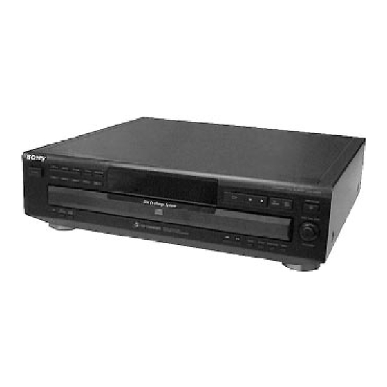
Photo : CDP-CE315
Model Name Using Similar Mechanism
CD Mechanism Type
Base Unit Type
Optical Pick-up Type
SPECIFICATIONS
Maximum
Load
output
impedance
level
2V
Over 10 kilohms
(at 50 kilohms)
–18 dBm
Wave length:
660nm
CDP-C160Z/C260Z/CE215/CE315
Australian Model
CDP-C250Z/C350Z/CE305/CE405
CDM27A2-5BD20
BU-5BD20
KSS-213BA/F-NP
General
Power requirements
Where purchased
US, Canadian
AEP, UK, CIS, Singapore
North European, East European
Australian
E
Power consumption
14W
430 × 120 × 385 mm
Dimensions (approx.)
(17 × 4 3/4 × 15 1/4 in.) incl. projecting parts
(w/h/d)
Mass (approx.)
5.4 kg (11 lbs 15 oz)
Supplied accessories
Audio cord (2 phono plugs–2 phono plugs) (1)
Remote commander (remote) (CDP-CE315 and CDP-C260Z
only)
Sony SUM-3 (NS) batteries (2) (CDP-CE315 and CDP-C260Z
only)
Design and specifications are subject to change without notice.
COMPACT DISC PLAYER
US Model
Canadian Model
CDP-C260Z/CE215/CE315
AEP Model
CDP-CE215/CE315
UK Model
E Model
CDP-CE315
Power requirements
120V AC, 60 Hz
220-230V AC, 50/60 Hz
240V AC, 50/60 Hz
110-120V, 220-240V
adjustable, 50/60 Hz
Advertisement
Table of Contents

Related Manuals for Sony CDP-C160Z


Summary of Contents for Sony CDP-C160Z
- Page 1 Audio cord (2 phono plugs–2 phono plugs) (1) level Remote commander (remote) (CDP-CE315 and CDP-C260Z only) LINE OUT Phono Over 10 kilohms Sony SUM-3 (NS) batteries (2) (CDP-CE315 and CDP-C260Z jacks (at 50 kilohms) only) DIGITAL OUT Optical –18 dBm...
-
Page 2: Table Of Contents
CRITIQUES POUR LA SÉCURITÉ DE FONCTIONNEMENT. NE COMPONENTS WITH SONY PARTS WHOSE PART NUMBERS REMPLACER CES COMPOSANTS QUE PAR DES PIÈSES SONY APPEAR AS SHOWN IN THIS MANUAL OR IN SUPPLEMENTS DONT LES NUMÉROS SONT DONNÉS DANS CE MANUEL OU PUBLISHED BY SONY. - Page 3 4-987- Check the antenna terminals, metal trim, “metallized” knobs, screws, and all other exposed metal parts for AC leakage. Check leakage as described below. CDP-C160Z US Model : 782-4π LEAKAGE CDP-C260Z US Model : 783-7π...
- Page 4 HOW TO OPEN THE DISC TRAY WHEN POWER SWITCH TURNS OFF Insert a tapering driver into the aperture of the unit bottom, and turn in the direction of arrow (to OUT direction). * To close the disc tray, turn the driver in the reverse direction (to IN direction).
-
Page 5: General
SECTION 1 GENERAL Identifying the Parts Front Panel !¡ !£ 1 23456 7 !™ !¢ @¢ @¡ !ª !¶ @∞ @£ @™ @º !• !§ !∞ !£ POWER switch DISC SKIP button !¢ CONTINUE button 6 OPEN/CLOSE button !∞ SHUFFLE button AMS knob !§... -
Page 6: Disassembly
SECTION 2 DISASSEMBLY Note : Follow the disassembly procedure in the numerical order given. 2-1. CASE, BOTTOM PLATE AND FRONT PANEL 4 Case 1 Two screws (M3 × 8) 3 Two screws (BV3 × 8) !º Two screws (BVTT3 × 8) 9 Flat type wire (9 core) 2 Two screws (MAIN board, to CN402) -
Page 7: Optical Pick-Up Block Assembly
2-3. OPTICAL PICK-UP BLOCK ASSEMBLY 2 Screw (PTPWH3 × 12) 3 Two screws (PTPWH2.6 × 6) 4 Two screws (PTPWH2.6 × 6) 8 Optical pick-up block assembly 6 Compression spring (BU) 1 Flat type wire (16 core) (BD board, to CN101) 5 Holder (BU) 7 Compression spring (BU) 2-4. -
Page 8: Electrical Block Checking
SECTION 3 ELECTRICAL BLOCK CHECKING Note : Note : A clear RF signal waveform means that the shape “ ◊ ” can CD Block is basically designed to operate without adjustment. Therefore, check each item in order given. be clearly distinguished at the center of the waveform. Use YEDS-18 disc (3-702-101-01) unless otherwise indicated. - Page 9 RF PLL Free-run Frequency Check Adjustment Location : Procedure : [ BD BOARD ] — Conductor Side — Connect frequency counter to test point (PLCK) with lead wire. frequency counter BD board TP (PLCK) (FE) (RF) (FEI) IC103 Turned Power switch on. (TE) Put the disc (YEDS-18) in to play the number five track.
-
Page 10: Diagrams
SECTION 4 DIAGRAMS 4-1. CIRCUIT BOARDS LOCATION BD BOARD TABLE MOTOR BOARD SENSOR BOARD LOADING MOTOR BOARD POWER SW BOARD KEY BOARD MAIN BOARD DISPLAY BOARD —... - Page 11 G E N E R A T O R P L M P L M C L O C K N O I S E S H A P E R 3 R D O R D E R H O L D ( X 1 ) D I T H E R S A M P L E I I R...
-
Page 12: Ic Pin Functions
4-9. IC PIN FUNCTIONS • IC101 DIGITAL SIGNAL PROCESSOR (CXD2545Q) Pin No. Pin Name Function SRON Sled drive output (Not used) SRDR Sled drive output SFON Sled drive output (Not used) TFDR Tracking drive output TRON Tracking drive output (Not used) TRDR Tracking drive output TFON... - Page 13 Pin No. Pin Name Function — Digital power supply ASYE Asymmetry circuit ON/OFF PSSL Audio data output mode selection input WDCK 48-bit slot D/A interface. Word clock. LRCK 48-bit slot D/A interface. LR clock. DATA DA 16 output when PSSL=1.48-bit slot serial data when PSSL=0 BCLK DA 15 output when PSSL=1.48-bit slot data when PSSL=0 64DATA...
- Page 14 Pin No. Pin Name Function XRST System reset DIRC Used in 1-track jump mode (+5v) SCLK SENS serial data read-out clock DFSW DFCT selection pin (Ground) ATSK Input pin for anti-shock (Ground) DATA Serial data input, supplied from CPU XLAT Latch input, supplied from CPU CLOK Serial data transfer clock input, supplied from CPU...
-
Page 15: Ic302 System Control (Cxp82324-082Q)
• IC302 SYSTEM CONTROL (CXP82324-082Q) Pin No. Pin Name Function BUS IN Not used. (Pull up) RM IN Remote control signal input ADJ mode setting pin CXD2545 latch output LD ON Laser diode ON output TSENS Table position sensor input PRGL CXD8567 latch output CXD2545/CXD8567 serial clock output... - Page 16 Pin No. Pin Name Function FL display tube segmant output 4 FL display tube segmant output 5 FL display tube segmant output 6 FL display tube segmant output 7 FL display tube segmant output 8 FL display tube segmant output 9 FL display tube segmant output 10 FL display tube segmant output 11 FL display tube segmant output 12...
-
Page 17: Exploded Views
4-987-779-01 WINDOW (FL) (C160Z/CE215) 3-703-685-21 SCREW (+BV 3X8) 4-987-779-11 WINDOW (FL) (C260Z/CE315) 3-704-366-01 SCREW (CASE) (M3X8) 4-977-589-01 BUTTON (POWER) X-4946-618-1 FOOT ASSY (US,CND) 3-008-600-01 EMBLEM (5-AR), SONY X-4946-641-1 FOOT ASSY (EXCEPT US,CND) 4-951-620-01 SCREW (2.6X8), +BVTP * 15 4-978-398-21 CUSHION 1-664-522-11 DISPLAY BOARD...
Need help?
Do you have a question about the CDP-C160Z and is the answer not in the manual?
Questions and answers