Table of Contents
Advertisement
Quick Links
SERVICE MANUAL
Ver 1.0 1999. 12
MICROFILM
SPECIFICATIONS
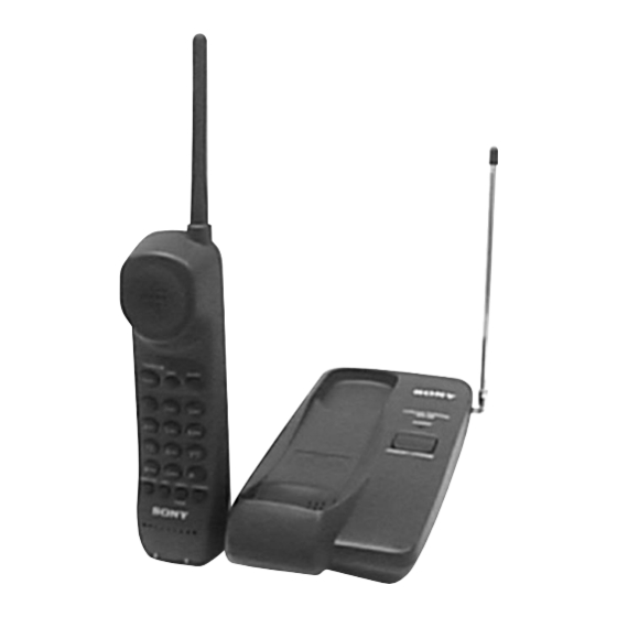
General
Frequency control
Crystal-controlled PLL
Operation mode
FM, duplex
Operation channel
10 channels
Supplied accessories
AC power adaptor AC-T56 (1)
Telephone line cord (1)
Rechargeable battery pack BP-T16 (1)
Screws (2)
Directories (2 sheets)
Handset
Power source
Rechargeable battery pack BP-T16
Battery life
Standby: Approx. 14 days
Talk:
Approx. 6 hours
Dimensions
Approx. 2
3/8
excluded (approx. 58 × 194 × 47 mm)
Antenna: Approx. 4
Mass
Approx. 7.8 oz (approx. 220 g), battery included
Base unit
Power source
DC 9V from AC power adaptor
Battery charging time
Approx. 12 hours
Dimensions
Approx. 5
1/4
excluded (approx. 132 × 56 × 220 mm)
Antenna: Approx. 12
Mass
Approx. 11 oz (approx. 310 g)
Design and specifications are subject to change without notice.
– 1 –
SPP-69/79
× 7
× 1
inches (w/h/d), antenna
3/4
7/8
inches (approx. 110 mm)
3/8
× 2
× 8
inches (w/h/d), antenna
1/4
3/4
inches (approx. 310 mm)
1/4
CORDLESS TELEPHONE
Singapore Model
Advertisement
Table of Contents

Related Manuals for Sony SPP-69


Summary of Contents for Sony SPP-69
- Page 1 SPP-69/79 SERVICE MANUAL Singapore Model Ver 1.0 1999. 12 SPECIFICATIONS General Frequency control Crystal-controlled PLL Operation mode FM, duplex Operation channel 10 channels Supplied accessories AC power adaptor AC-T56 (1) Telephone line cord (1) Rechargeable battery pack BP-T16 (1) Screws (2)
-
Page 2: Table Of Contents
COMPONENTS IDENTIFIED BY MARK 0 OR DOTTED LINE WITH MARK 0 ON THE SCHEMATIC DIAGRAMS AND IN THE PARTS LIST ARE CRITICAL TO SAFE OPERATION. REPLACE THESE COMPONENTS WITH SONY PARTS WHOSE PART NUMBERS APPEAR AS SHOWN IN THIS MANUAL OR IN SUPPLEMENTS PUBLISHED BY SONY. -
Page 3: General
SECTION 1 GENERAL This section is extracted from instruction manual. – 3 –... - Page 4 – 4 –...
- Page 5 – 5 –...
-
Page 6: Disassembly
SECTION 2 DISASSEMBLY Note : Follow the disassembly procedure in the numerical order given. 2-1. CABINET (LOWER) (BASE UNIT) 1 P 3x10 2 P 3x10 4 cabinet (lower) 3 CN301 2-2. CABINET (REAR) (HANDSET) 3 claws 4 claw 1 battery case lid assy 2 BTP 2.6x10 5 cabinet (rear) –... -
Page 7: Test Mode
SECTION 3 TEST MODE BASE UNIT SECTION MACHINE TEST MODE Set the Test Mode: 1. With one of the CH setting terminals in “H” input state, cause MANUAL TEST MODE Reset of Power ON. Equipment enters machine test mode. Set the Test Mode: 2. - Page 8 Channel Setting: During startup in machine test mode, make the following channel settings by loading the terminal input data. Pin No. TX frequency RX frequency (MHz) (MHz) Channel (TP61) (TP62) (TP63) (TP64) 46.610 49.670 46.630 49.845 46.670 49.860 46.710 49.770 46.730 49.875 46.770...
-
Page 9: Handset Section
HANDSET SECTION MACHINE TEST MODE Set the Test Mode: 1. When power on reset is applied while a “H” (high) is input the MANUAL TEST MODE TEST SW (TP43) terminal (IC501 r; pin), the RING (Level Set the Test Mode: H, 500 msec) sounds. - Page 10 Channel Setting: During startup in machine test mode, make the following channel settings by loading the terminal input data. Pin No. TX frequency RX frequency ROW5 ROW4 ROW3 ROW2 ROW1 (MHz) (MHz) Channel (TP13) (TP14) (TP15) (TP16) (TP17) 48.760 43.720 48.840 43.740 48.860...
- Page 11 Key Processing (Setting the Manual Test Mode) : 1. (Upper position) (Lower position) Set with #. 2. 3X# can be substituted with X . Upper position Lower position QUIT 10 ch 20 ch Batt Alarm KEY TEST 1 ch 11 ch 21 ch CHARGE DET 2 ch...
-
Page 12: Electrical Adjustments
SECTION 4 ELECTRICAL ADJUSTMENTS BASE UNIT SECTION RX SECTION ADJUSTMENT RX LEVEL Adjustment Note: Note: • Apply 9V dc from regurated DC power supply. • Perform the adjustment at TEST3CH (28CH : 49.910 MHz) as a • Perform the adjustment at TEST3CH (28CH : 49.910 MHz) as a rule. - Page 13 Adjustment Location : – base main board (component side) – L101 FL101 RV101 – base main board (conductor side) – TP104 TP19 TP105 TP23 IC101 IC501 – 13 –...
-
Page 14: Handset Section
HANDSET SECTION RX SECTION ADJUSTMENT RX LEVEL Adjustment Note: Note: • Apply 3.6 V dc from regurated DC power supply. • Perform the adjustment at TEST1CH (26CH : 43.780 MHz) as a • Perform the adjustment at TEST1CH (26CH : 43.780 MHz) as a rule. - Page 15 Adjustment Location : – hand main board (side A) – RV101 L102 FL101 – hand main board (side B) – TP27 TP26 IC501 IC101 TP30 – 15 –...
-
Page 16: Diagrams
SECTION 5 DIAGRAMS 5-1. IC PIN DESCRIPTIONS • IC501 SB662104A-4L63-TLM (SYSTEM CONTROL) (BASE UNIT) Pin No. Pin Name Pin Description Strobe signal output to PLL. DATA Serial data output to PLL. Serial clock output to PLL. RX-DATA RX data input SIG-IN RSSI/PLL-LOCK signal input (L: RSSI, H: PLL-LOCK) H-MUTE... - Page 17 • IC501 SH66356C-4L62 (SYSTEM CONTROL) (HANDSET) Pin No. Pin Name Pin Description TEST CH Test mode channel control output (L: Active) KEY LED Key LED ON/OFF control output (L: ON) (Fixed at “H” in this set.) SIG-IN RSSI/PLL-LOCK signal input (L: RSSI, H: PLL-LOCK) PLL-STB Strobe signal output to PLL.
-
Page 18: Block Diagram -Base Unit Section
SPP-69/79 5-2. BLOCK DIAGRAM — BASE UNIT SECTION — ANT1 TELESCOPIC ANTENNA D101 B+ (+5.2V) FL101 460kHz MJ201 MIX, IF AMP, DET RX LEVEL EXPANDER LINE IC101 (1/3) IC101 (2/3) D205 BPF1 CF101 RECT 46MHz 460kHz B+ (+5.2V) T201 RECEIVER... -
Page 19: Block Diagram -Handset Section
SPP-69/79 5-3. BLOCK DIAGRAM — HANDSET SECTION — ANT2 B+ (+3.6V) HELICAL ANTENNA S101 FL101 460kHz MIX, IF AMP, DET RX LEVEL EXPANDER IC101 (1/3) IC101 (2/3) RECEIVER BPF1 CF101 49MHz 460kHz RECE-IN QUAD SPEAKER – CF102 E-MUTE 10.68MHz IF-IN... -
Page 20: Printed Wiring Board -Base Unit Section
SPP-69/79 5-4. PRINTED WIRING BOARD — BASE UNIT SECTION — • Semiconductor Location Ref. No. Location D101 D201 D203 D204 D205 D206 D207 D208 D301 D401 D501 IC101 IC301 G-10 IC302 IC303 IC501 PH201 PH202 Q201 Q202 Q203 Q302 F-10... -
Page 21: Schematic Diagram -Base Unit Section
SPP-69/79 5-5. SCHEMATIC DIAGRAM — BASE UNIT SECTION — • Refer to page 31 for IC Block Diagram. – 25 – – 26 –... -
Page 22: Printed Wiring Board -Handset Section
SPP-69/79 5-6. PRINTED WIRING BOARD — HANDSET SECTION — • Semiconductor Location Ref. No. Location Ref. No. Location Ref. No. Location D502 A-10 D202 B-13 D504 A-11 D301 A-13 Q201 Note: (D401) IC101 Q301 A-13 • X : parts extracted from the component side. -
Page 23: Schematic Diagram -Handset Section
SPP-69/79 5-7. SCHEMATIC DIAGRAM — HANDSET SECTION — • Refer to page 31 for Note. – 29 – – 30 –... -
Page 24: Exploded Views
SECTION 6 EXPLODED VIEWS Note on Schematic Diagram: NOTE: • All capacitors are in µF unless otherwise noted. pF: µµF • The mechanical parts with no reference • -XX and -X mean standardized parts, so • Accessories and packing materials and 50 WV or less are not indicated except for electrolytics number in the exploded views are not supplied. -
Page 25: Handset Section
6-2. HANDSET SECTION MIC1 ANT2 Ref. No. Part No. Description Remark Ref. No. Part No. Description Remark X-3377-828-1 LID ASSY (G), BATTERY CASE * 58 3-033-764-01 CUSHION (BUZZER) 3-038-923-01 CABINET (REAR) 1-771-708-11 SWITCH, RUBBER KEY (HAND) (69) * 53 A-3622-383-A HAND MAIN BOARD, COMPLETE (69) 1-771-708-21 SWITCH, RUBBER KEY (HAND) (79) * 53 A-3622-385-A HAND MAIN BOARD, COMPLETE (79) -
Page 26: Electrical Parts List
SECTION 7 BASE MAIN ELECTRICAL PARTS LIST NOTE: • Due to standardization, replacements in • Items marked “*” are not stocked since The components identified by mark 0 or dotted line with mark the parts list may be different from the they are seldom required for routine service. - Page 27 BASE MAIN Ref. No. Part No. Description Remark Ref. No. Part No. Description Remark C504 1-163-104-00 CERAMIC CHIP 30PF JR16 1-216-296-00 SHORT C505 1-163-137-00 CERAMIC CHIP 680PF JR17 1-216-296-00 SHORT C506 1-163-104-00 CERAMIC CHIP 30PF JR18 1-216-296-00 SHORT JR19 1-216-296-00 SHORT <...
- Page 28 BASE MAIN Ref. No. Part No. Description Remark Ref. No. Part No. Description Remark 1-216-069-00 METAL CHIP 6.8K 1/10W R404 1-216-005-00 METAL CHIP 1/10W 1-216-264-00 RES-CHIP 560K 1/8W R405 1-216-025-11 RES-CHIP 1/10W 1-216-097-11 RES-CHIP 100K 1/10W R406 1-216-073-00 METAL CHIP 1/10W 1-216-057-00 METAL CHIP 2.2K...
- Page 29 HAND MAIN Ref. No. Part No. Description Remark Ref. No. Part No. Description Remark A-3622-383-A HAND MAIN BOARD, COMPLETE (69) C121 1-165-319-11 CERAMIC CHIP 0.1uF A-3622-385-A HAND MAIN BOARD, COMPLETE (79) C122 1-163-235-11 CERAMIC CHIP 22PF C123 1-165-319-11 CERAMIC CHIP 0.1uF *************************** C124...
- Page 30 HAND MAIN Ref. No. Part No. Description Remark Ref. No. Part No. Description Remark D403 8-719-059-94 LED SML-010MT-T86 (79) < MICROPHONE > D404 8-719-059-94 LED SML-010MT-T86 (79) D501 8-719-059-87 LED SLR-342VRTB7 (TALK/BATT LOW) MIC1 1-542-118-11 MICROPHONE, ELECTRET CONDENSER D502 8-719-914-43 DIODE DAN202K D504 8-719-941-04 DIODE SB007-03CP <...
- Page 31 HAND MAIN Ref. No. Part No. Description Remark Ref. No. Part No. Description Remark R130 1-216-077-11 RES-CHIP 1/10W < VIBRATOR > R141 1-216-206-00 RES-CHIP 2.2K 1/8W R142 1-216-057-00 METAL CHIP 2.2K 1/10W X101 1-760-326-11 VIBRATOR, CRYSTAL (10.2MHz) R144 1-216-061-00 METAL CHIP 3.3K 1/10W X501...
- Page 32 SPP-69/79 Sony Corporation 1999L04012-1 9-927-627-11 Personal Audio Division Company Printed in Japan ©1999. 12 – 40 – Published by General Engineering Dept.
Need help?
Do you have a question about the SPP-69 and is the answer not in the manual?
Questions and answers