Table of Contents
Advertisement
Quick Links
SERVICE MANUAL
Ver 1.1 2001.12
General
Operating frequency
Base phone: 902-905 MHz (310µW)
Hand set:
Operating channel
10 channels
Dial signal
Tone, 10 PPS (pulse) selectable
Supplied accessories
AC power adaptor AC-T122
Telephone line cord
Rechargeable battery pack BP-T18
Wall bracket
Directory
Handset
Power source
Rechargeable battery pack BP-T18
Battery life
Standby: Approx. 7 days
Talk:
Dimensions
Approx. 2
antenna excluded
(approx. 55 x 47 x 183 mm)
Antenna: Approx. 1
(approx. 34 mm)
Mass
Approx. 7.7 oz (approx. 220 g), battery
included
Sony Corporation
9-873-224-02
2001L0500-1
Personal Audio Company
C 2001.12
Published by Sony Engineering Corporation
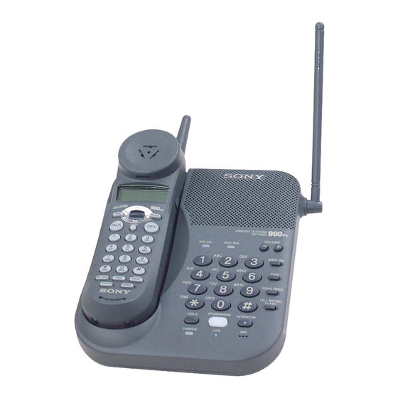
SPP-N1025/N1026
Photo: SPP-N1025
SPECIFICATIONS
925-928 MHz (400µW)
Approx. 7 hours
1
7
1
⁄
x 1
⁄
x 7
⁄
inches (w/h/d),
4
8
4
3
⁄
inches
8
Base phone
Power source
DC 9V from AC power adaptor AC-T122
Battery charging time
Approx. 12 hours
Dimensions
1
1
Approx. 7 x 2
⁄
x 7
⁄
inches (w/h/d),
4
2
antenna excluded
(approx. 175 x 57 x 190 mm)
1
Antenna: Approx. 6
⁄
inches
8
(approx. 153 mm)
Mass
Approx. 13.5 oz (approx. 382 g), wall
bracket excluded
Design and specifications are subject to
change without notice.
CORDLESS TELEPHONE
US Model
SPP-N1025
Canadian Model
SPP-N1026
Advertisement
Table of Contents

Related Manuals for Sony SPP-N1025


Summary of Contents for Sony SPP-N1025
- Page 1 (approx. 55 x 47 x 183 mm) Antenna: Approx. 1 ⁄ inches (approx. 34 mm) Mass Approx. 7.7 oz (approx. 220 g), battery included CORDLESS TELEPHONE Sony Corporation 9-873-224-02 2001L0500-1 Personal Audio Company C 2001.12 Published by Sony Engineering Corporation...
-
Page 2: Table Of Contents
OPERATION. REPLACE THESE COMPONENTS WITH DE FONCTIONNEMENT. NE REMPLACER CES COM- SONY PARTS WHOSE PART NUMBERS APPEAR AS POSANTS QUE PAR DES PIÈCES SONY DONT LES SHOWN IN THIS MANUAL OR IN SUPPLEMENTS PUB- NUMÉROS SONT DONNÉS DANS CE MANUEL OU LISHED BY SONY. -
Page 3: Servicing Notes
SPP-N1025/N1026 SECTION 1 SERVICING NOTES NOTE FOR REPLACEMENT OF THE EEPROM ABOUT U7 ON THE BASE MAIN BOARD U7 (Part No. 6-800-854-01) on the BASE MAIN board which has The ID cord is written in the EEPROM. When replacing the EEPROM, U6 on the BASE MAIN board and board shape as shown below, is different from regular ICs in shape. - Page 4 HAND MAIN boards have been changed. When a new type board is damaged or out of order, do not repair SPP-N1025 : Serial No. 0207433 or alter that board, but replace with an former type board (BASE MAIN SPP-N1026 : Serial No. A0106801 or later board : Part No.
-
Page 5: General
SPP-N1025/N1026 SECTION 2 This section is extracted from instruction manual. GENERAL Identifying the parts Refer to the pages indicated in parentheses for details. Base Phone 1 VOICE MAIL lamp (p. 47) 9 INTERCOM button/lamp qh Antenna (p. 7, 49) (p. 36) Flashes when you have messages. -
Page 6: Disassembly
SPP-N1025/N1026 SECTION 3 DISASSEMBLY • This set can be disassembled in the order shown below. 3-1. DISASSEMBLY FLOW HAND MAIN board H/S rear assy H/S FRT assy Base bottom BASE MAIN board Note: Follow the disassembly procedure in the numerical order given. -
Page 7: H/S Frt Assy
SPP-N1025/N1026 3-3. H/S FRT ASSY 1 screw (BTP2.6 × 8) 3 screw (BTP2.6 × 8) 4 two screws (P2 × 5) 6 H/S FRT assy 3-4. HAND MAIN BOARD 5 screw (BTP2.6 × 8) 6 RF unit (hand) 8 receiver BKT 4 Remove twelve solders. -
Page 8: Base Bottom
SPP-N1025/N1026 3-5. BASE BOTTOM 2 claw 1 five screws (P3 × 12) 3 base bottom 2 claw 3-6. BASE MAIN BOARD 6 two screws 8 BASE MAIN board (BTP2.6 × 8) 5 Remove two solders. 3 screw (P3 × 6) -
Page 9: Test Mode
SPP-N1025/N1026 SECTION 4 TEST MODE Introduction Condition: Press the key. The manual test mode can be used for testing the RF and audio Operation: TX data on, it only send security code change command sections of the base unit and handset. The manual test mode is out if the transmitter power ON. - Page 10 SPP-N1025/N1026 [SPEED] Condition: Press the key. Operation: Increment channel by 1. Operation: Cleaar all two touch memory from EEPROM. Indication: CH=CH+1 Indication: Beep tone is emitted. Operation: Mute TX audio path. [SPEAKERPHONE] Condition: Press the key. Indication: TxM=1 Operation: Release thetestmode.
- Page 11 SPP-N1025/N1026 Security Code Synchronization The following procedures should be followed if the security codes of both unit do not match to each other. 1. Put the handset into manual test mode, making sure the channel is set at 14 (default) out of 0 to 29.
- Page 12 SPP-N1025/N1026 MEMO...
-
Page 13: Diagrams
SPP-N1025/N1026 SECTION 5 DIAGRAMS 5-1. BLOCK DIAGRAM – BASE UNIT Section – TEL LINE SWITCH RF UNIT U13 (3/4) LINE TRANSFORMER AF AMP BUFFER LINE TX AUDIO (FOR TX) U2 (1/4) TEL LINE SWITCH U13 (2/4) AF AMP HOOK ON/OFF... -
Page 14: Block Diagram - Handset Section
SPP-N1025/N1026 5-2. BLOCK DIAGRAM – HANDSET Section – RF UNIT • SIGNAL PATH : TX TX DATA 29 TX DATA : RX PLL EN 14 PLL EN LCD1 PLL CLK 15 PLL CLK LIQUID CRYSTAL 16 PLL I2C DATA PLL I2C DATA... -
Page 15: Note For Printed Wiring Boards And Schematic Diagrams
SPP-N1025/N1026 5-3. NOTE FOR PRINTED WIRING BOARDS AND SCHEMATIC DIAGRAMS • IC Block Diagrams – BASE MAIN Board – Note on Printed Wiring Board: Note on Schematic Diagram: • All capacitors are in µF unless otherwise noted. pF: µµF • X : parts extracted from the component side. -
Page 16: Schematic Diagram - Base Main Board (1/2)
SPP-N1025/N1026 5-4. SCHEMATIC DIAGRAM – BASE MAIN Board (1/2) – • • See page 15 for Waveforms. See page 15 for IC Block Diagram. R127 RINGER PLL EN ROW0 RI_LO ROW1 RI_LO HIGH RI_HI ROW2 RI_HI ROW3 ROW4 ROW5 SYSTEM CONTROLLER... -
Page 17: Schematic Diagram – Base Main Board (2/2)
SPP-N1025/N1026 5-5. SCHEMATIC DIAGRAM – BASE MAIN Board (2/2) – • See page 15 for IC Block Diagrams. R116 EC13 4.7k 0.01 5.1k SPEAKER AMP EC19 KA8602B EC22 VOICE SPEAKERPHONE EC18 EC14 RIPPLE INPUT+ U4082B 100k INPUT- MUTE R114 1000p... -
Page 18: Printed Wiring Board - Base Main Board
SPP-N1025/N1026 5-6. PRINTED WIRING BOARD – BASE MAIN Board – BASE MAIN BOARD R134 R133 Z4 R52 R129 R135 R131 R130 CHARGE TERMINAL R132 LINE LINE TRANSFORMER – E C B DC IN 9V EC20 MIC101 R121 R120 R104 EC17... -
Page 19: Printed Wiring Board - Base Key Board
SPP-N1025/N1026 5-7. PRINTED WIRING BOARD – BASE KEY Board – 5-8. SCHEMATIC DIAGRAM – BASE KEY Board – (Page 17) • Semiconductor (Page 18) Location Ref. No. Location LED1 LED2 LED4 LED6 LED7 LED8... -
Page 20: Printed Wiring Board - Hand Main Board
SPP-N1025/N1026 5-9. PRINTED WIRING BOARD – HAND MAIN Board – • Semiconductor Location Ref. No. Location CHARGE TERMINAL – DISPLAY MODULE 3.6V 600mAh... -
Page 21: Schematic Diagram - Hand Main Board
SPP-N1025/N1026 5-10. SCHEMATIC DIAGRAM – HAND MAIN Board – • See page 15 for Waveforms. V BAT 24WC32 TX DATA COM0 COM1 100k COM2 CAR DET/LOW BAT COM3 COM4 PLL EN UNIT COM5 PLL CLK COM2 SEG28 COM6 PLL I2C DATA... -
Page 22: 5-11. Ic Pin Function Description
SPP-N1025/N1026 5-11. IC PIN FUNCTION DESCRIPTION • BASE MAIN BOARD U7 TMP87CH41U (SYSTEM CONTROLLER) Pin No. Pin Name Description Pin No. Pin Name Description MIC MUTE Microphone muting on/off control signal output to the voice speakerphone (U4) “H”: muting on... - Page 23 SPP-N1025/N1026 • HAND MAIN BOARD U2 TMP87C807U-3CR4 (SYSTEM CONTROLLER) Description Pin No. Pin Name — Ground terminal Main system clock input terminal (8 MHz) XOUT Main system clock output terminal (8 MHz) TEST Setting terminal for the test Not used (fixed at “L”) —...
-
Page 24: Exploded Views
SPP-N1025/N1026 SECTION 6 EXPLODED VIEWS NOTE: • -XX and -X mean standardized parts, so they • Items marked “*” are not stocked since they may have some difference from the original are seldom required for routine service. Some one. delay should be anticipated when ordering •... -
Page 25: Base Set Section
SPP-N1025/N1026 6-2. BASE SET SP101 supplied MIC101 Ref. No. Part No. Description Remark Ref. No. Part No. Description Remark 3-233-544-01 FOOT, RUBBER 3-233-542-01 ANT B/S 3-230-095-01 BASE BOTTOM (N1025) 3-236-106-01 FROM, SPK CUSHION BS 3-236-295-01 BASE CASE BTM (N1026) A-3062-577-A BASE RF UNIT... -
Page 26: Electrical Parts List
SPP-N1025/N1026 SECTION 7 ELECTRICAL PARTS LIST BASE KEY BASE MAIN NOTE: • Due to standardization, replacements in the • Items marked “*” are not stocked since they The components identified by mark 0 or dotted line with mark parts list may be different from the parts speci- are seldom required for routine service. - Page 27 SPP-N1025/N1026 BASE MAIN Ref. No. Part No. Description Remark Ref. No. Part No. Description Remark EC11 1-126-961-11 ELECT 2.2uF 1-216-845-11 METAL CHIP 100K 1/16W EC12 1-126-947-11 ELECT 47uF 1-216-843-11 METAL CHIP 1/16W EC13 1-126-964-11 ELECT 10uF 1-216-841-11 METAL CHIP 1/16W...
- Page 28 SPP-N1025/N1026 Ver 1.1 BASE MAIN HAND MAIN Ref. No. Part No. Description Remark Ref. No. Part No. Description Remark 1-216-833-11 METAL CHIP 1/16W 8-759-013-86 IC MC74HC4066F 1-216-864-11 METAL CHIP 1/16W 8-759-658-47 IC KA8602D 1-216-847-11 METAL CHIP 150K 1/16W < VIBRATOR >...
- Page 29 SPP-N1025/N1026 Ver 1.1 HAND MAIN Ref. No. Part No. Description Remark Ref. No. Part No. Description Remark 8-719-059-44 LED TF541M (KEY BACK LIGHT) (N1026) 1-216-802-11 RES-CHIP 1/16W 8-719-029-30 DIODE BAS16-215 (N1026) 1-216-802-11 RES-CHIP 1/16W < CAPACITOR > (N1026) 1-124-589-11 ELECT...
-
Page 30: Revision History
SPP-N1025/N1026 REVISION HISTORY Clicking the version allows you to jump to the revised page. Also, clicking the version at the upper right on the revised page allows you to jump to the next revised page. Ver. Date Description of Revision 2001.12...
Need help?
Do you have a question about the SPP-N1025 and is the answer not in the manual?
Questions and answers